#PCB Power
Explore tagged Tumblr posts
Visit Tumblr Blog
Explore Tumblr blogs with no restrictions, modern design and the best experience.
Last Seen Tumblr Blogs


Fun Fact
Tumblr posted its first advertisements in May 2012 and subsequently earned $13M in revenue.
Text
Top 15 PCB Board Manufacturers in USA

When it comes to building reliable electronics, choosing the right PCB board manufacturer in USA is critical. Whether you’re a startup, engineer, OEM, or tech company, having a dependable partner for printed circuit board fabrication and assembly ensures faster production, fewer errors, and better results.
In this blog, we list the Top 15 PCB board manufacturers in the USA known for high-quality PCB fabrication, assembly, and fast delivery. These companies are widely searched and trusted across various industries — from medical to aerospace, IoT, automotive, and industrial applications.
1. PCB Power
PCB Power is one of the most trusted names among PCB board manufacturers USA. With over two decades of industry experience, PCB Power offers quick-turn PCB fabrication, full turnkey assembly, and components sourcing — all under one roof.
As a USA-based PCB company, they focus on delivering high-quality single, double, and multilayer PCBs with fast turnaround and competitive pricing. Whether you’re building prototypes or mass production, PCB Power’s online ordering system makes it easy to get instant quotes, track orders, and communicate with real engineers.
Key Features:
US-based production for fast and reliable delivery
ISO-certified processes for superior quality
Advanced manufacturing for high-density, multilayer PCBs
Turnkey assembly and BOM handling
Expert support for startups, engineers, and OEMs
If you’re looking for a complete PCB manufacturing solution in the USA, PCB Power should be your first stop.
2. Advanced Circuits
Advanced Circuits is one of the largest and oldest PCB manufacturers in the United States. Known for high-quality prototypes and low-to-medium volume production, they serve industries like aerospace, defense, and telecom.
They offer same-day and next-day shipping options and have their own in-house manufacturing for consistent quality.
3. Sierra Circuits
Sierra Circuits is a full-service PCB company specializing in quick-turn fabrication and assembly. They’re well-known for their high-performance HDI PCBs, rigid-flex boards, and support for complex designs. Sierra Circuits is ideal for companies looking for technical precision and tight tolerances.
4. Sunstone Circuits
Sunstone Circuits has built a reputation for delivering reliable prototype PCBs and small-batch orders. Their online design tools and instant quote system are ideal for hobbyists, startups, and small engineering teams. Their US-based manufacturing ensures high quality and fast shipping.
5. Bay Area Circuits
Located in California, Bay Area Circuits serves the Silicon Valley tech community with rapid prototyping, fabrication, and assembly services. They are experts in small-run production and serve various industries including medical, aerospace, and communications.
6. Rush PCB Inc.
Rush PCB Inc. offers full turnkey PCB services, including design, manufacturing, and assembly. They specialize in multilayer, flex, and rigid-flex PCBs with quick-turn options. Their experienced team supports everything from prototypes to volume production.
7. Custom Circuit Boards
Based in Arizona, Custom Circuit Boards provides high-quality PCBs for engineers and hardware startups. They focus on fast production and specialize in multilayer boards, thick copper PCBs, and RF designs.
8. Imagineering Inc.
Imagineering Inc. offers both PCB fabrication and assembly with ISO 9001 and AS9100 certifications. They serve demanding industries like medical and aerospace and are known for excellent quality and fast lead times.
9. Epec Engineered Technologies
Epec is a full-service provider offering custom PCB manufacturing, flexible circuits, and battery packs. With decades of experience, they provide engineered solutions for complex applications and tight deadlines.
10. APCT Inc.
APCT is known for high-speed, high-density interconnect PCBs. They support quick-turn and production-scale manufacturing. Their specialties include aerospace and defense-grade boards with rigorous quality requirements.
11. OnBoard Circuits
OnBoard Circuits offers affordable PCB prototyping, fabrication, and assembly with domestic and offshore capabilities. They are known for great customer support and fast delivery for small to medium volume orders.
12. Millennium Circuits Limited (MCL)
MCL provides reliable PCBs including rigid, flex, and rigid-flex boards. They serve industries like telecom, industrial, and medical, offering fast turnaround times and excellent pricing.
13. TechnoTronix
TechnoTronix offers advanced PCB manufacturing and assembly solutions with a strong focus on precision and fast lead times. They work with both small businesses and large enterprises, offering everything from basic to complex PCB designs.
14. RedBoard Circuits
RedBoard Circuits provides quality PCBs with a focus on customer service and quick delivery. They offer a wide range of PCB types including FR4, aluminum, and Rogers materials.
15. ALLPCB USA
ALLPCB USA offers cost-effective PCB solutions with a quick-turn focus. They provide both prototype and production runs and serve customers looking for affordable yet reliable circuit boards.
Choose the Best PCB Manufacturer for Your Needs
Selecting the right PCB board manufacturer in USA can be the difference between a successful project and costly delays. Whether you need fast prototyping, volume production, or full turnkey PCB assembly, each of these top 15 manufacturers brings something unique to the table.
However, if you’re looking for a complete solution with fast delivery, reliable quality, and competitive pricing — PCB Power is a clear leader. With US-based manufacturing, expert support, and a user-friendly online ordering platform, PCB Power makes your PCB journey seamless from design to delivery.
0 notes
Text
The Role of Flexible PCB Design in Next-Generation Robotics
Robotics and automation are not buzzwords anymore. We all witness the latest flying robots, auto-balancing AGVs, and industrial heavy collaborative robots that are revolutionizing the way we work. But do you know that PCBs are the “brain” of these technology marvels?
With the exponential demand for robotics in every field, the demand for smaller, lighter, more flexible electronic components, especially flex PCBs, is rapidly increasing. According to the International Federation of Robotics, there was a 48% increase in professional service robot sales globally by 2022. In such a scenario, flexible printed circuit boards (PCBs) have become the cornerstone of this transformation. Their special construction and ability are crucial for addressing the design difficulties given by next-generation robotics.
This article will explore how flexible PCB design is transforming robotics and what that implies for PCB manufacture.
Why Robotics Need Flexible PCBs
Unlike conventional rigid PCBs, flexible PCBs are designed to bend and twist, which creates countless opportunities for integrating electronics into the intricate forms and motions needed for robotic applications. For robotics, where designs generally call for flexibility and durability, flex PCBs, which can manage movement and fit into small areas, are perfect.
Key Benefits of Flexible PCB Design for Robotics
Flex PCBs are specially designed to focus on some key benefits that are essential for robotics and complex electronic devices. Some of the noteworthy advantages are:
Adaptability: Flexible PCBs can fit the form of the robotic component, therefore enabling designers to create thinner, lighter systems without compromising performance.
Durability: For robots with moving parts, these boards are perfect since they can absorb stress created during motion and vibration.
Space optimization: By reducing the need for connectors and bulky wiring, flexible PCBs free up valuable space and reduce the weight of the robot.
Enhanced reliability: High-performance robotics depend on fewer sources of failure. Flex PCBs reduce the requirements of connectors and bulky wirings, and therefore, they improve the robot's reliability.
Applications of Flexible PCBs in Robotics
From simple consumer devices to sophisticated industrial machines, flexible PCBs are fast taking the stage in many different robotic applications. Here is where flexible PCB manufacturing is taking the front stage:
Wearable Robots: Wearable robots are used in medical and fitness applications, and they require lightweight, comfortable designs. Flex PCBs make it possible for these devices to bend and contour to the user's body.
Drones and autonomous vehicles: Autonomous cars and drones call for lightweight parts that can withstand stress from continuous motion and fit small areas. Flexible PCBs enable maximum efficiency and help to reduce weight.
Industrial robots: Flexible PCBs can withstand the wear and tear of motion without compromising on performance. Therefore, it becomes highly dependable without sacrificing space for robotics undertaking repetitive tasks.
Important Considerations in Robotics Flexible PCB Design
Flexible PCB design for robotics presents certain difficulties. These are some crucial elements to consider:
Selection of Materials
Flexibility, durability, and heat resistance depend on the selected materials; hence, they are quite important. Because of its heat resistance, flexibility, and durability, polyimide is a common choice for flexible PCB manufacture.
Thickness and Layer Count
The number of layers in a flex PCB might range from one to many. The design requirements for the robot will dictate the optimal balance between physical flexibility and usefulness since adding more layers can limit its adaptability.
Copper Traces and Bend Radius
Careful design of copper traces in a flexible PCB helps to prevent cracks or breakage. Ensuring that traces follow a specific bend radius can help maintain the board's integrity during movement.
Component Placement
During operations, robots experience shocks and vibrations, so it's crucial to strategically place components and reinforce areas prone to bending. This lowers the possibility of component failure in high-stress environments.
Final Thoughts: Embracing Flexible PCBs into Your Robotic Designs
As it offers the adaptability, longevity, and efficiency required for modern, complicated applications, flexible PCB design plays an obvious role in robotics. As a PCB manufacturer, you can broaden the capabilities of robotics by learning about and making use of flex PCBs.
Including flexible PCBs in robotic designs not only creates more space-efficient, robust machines but also helps you to be in front of a market where innovation is vital. Adaptable electronics will surely define the direction of robotics going forward; flexible PCB fabrication has the power to propel these developments ahead.
PCB Power is your one-stop solution, providing premium, durable PCBs to support all technological advancements such as RoboticsLooking for a reliable flex PCB manufacturer for your project? Email us at [email protected] or call us at +1(818) 886 8900. Read More: The Role of Flexible PCB Design in Next-Generation Robotics
0 notes
Text


mashing together my two teenage years interests for dopamine
#johndirk#dirkjohn#homestuck#john egbert#dirk strider#my art#touhoustuck#just a funny little au because some of the parallels and ways character powers reflect eachother is fun#john is in no way as manipulative or a mastermind as yukari but his retcon powers are a very interesting vessel for yukaris gap powers#especially when his hand stuck out in a bunch of pages lol i like to imagine if he could master the powers it would let him do her teleport#around and spy nonsense but he'd just use it to be a class a prankster and for magic tricks#on the other hand yuyuko and dirk have an interesting parallel but one that is more like...the entire point is the culmination of#their characters despite the way they have these splinters. like yuyuko isnt nearly as fragmented as dirk but#theres a distinction between the yuyuko who was alive and the yuyuko whos dead and what she becomes after#its unclear if post PCB shes aware shes the one who sealed the saigyouji ayakashi away but she also just thinks its better for her#not to go down that rabbithole. she'd probably become worse if she did and with dirk he has that clarity with dave when they talk that like#even if there are worse versions of him out there. the fact he thinks and stops before proceeding separates him and i like to think that#is something he takes to heart with him post canon to stop beating himself up so much. umh also soul powers = ghost powers lalala#just silly and self indulgent tbh like im not extrapolating or translating backstories but in this au its fun to think o#humans turning into youkai like yukari used to be human and so did yuyuko. john and dirk used to be human and went godtier...anyways
50 notes
·
View notes
Text
What's new?
🚀 Pimoroni Tiny 2350 – Mini RP2350 dev board with 4MB Flash. 🔌 Pimoroni Pico Plus 2 – Pico-shaped RP2350 board with pins. 📡 Pimoroni Pico Plus 2 W – Wireless-ready RP2350 dev board. 💡 Pimoroni Tiny FX W – Wireless LED effects kit. ⚡ Adafruit TPS65131 – Split power supply (+/-6V to +/-15V).
adafruit.com/new!
#pimoroni#adafruit#rp2350#developmentboard#electronics#maker#tech#hardware#embedded#iot#wireless#led#power#flashmemory#diy#innovation#opensource#coding#raspberrypi#devkit#engineering#pcb#robotics#hobbyelectronics#gadgets#electronicsprojects#microcontroller#programming#linux#python
5 notes
·
View notes
Text
Certified Agilent 3070 ICT System Available online

Meet our latest range of ICT systems, Agilent 3070. This has been designed meticulously to provide you with optimal performance. Moreover, each system comes with a warranty and dedicated support. So, whether you’re upgrading, replacing, or expanding your testing capabilities, we have the right solution. Visit our website todayhttps://equip-test.com to order an Agilent 3070 ICT system and experience how your production workflow has dramatically improved! If you have any questions about this product, you can reach us at +361 533 3165.
0 notes
Text
https://www.futureelectronics.com/p/interconnect--automotive-connectors/2286014-2-te-connectivity-3083634
Automotive connector types, Wire Connectors, push in wire connectors
TPA LED ASSY
#Connectors#Automotive Connectors#2286014-2#TE Connectivity#Wire Connectors#push in wire connectors#electrical connector#Board-to-Board Connectors#cable Connector#PCB power connectors#cable connectors#Industrial electrical connectors
1 note
·
View note
Text
youtube
Würth Elektronik: REDCUBE Terminals (Innovative High Power Contacts)
https://www.futureelectronics.com/resources/featured-products/wurth-elektronik-redcube-terminals . REDCUBE terminals are the most reliable high-power contacts on the PCB level. Low contact resistance guarantees minimum self-heating. Four different designs cover all leading processing technologies and offer a wide range of applications. https://youtu.be/8EjH-SM1azE
#Wurth#REDCUBE Terminals#High Power Contacts#PCB Level#Low Contact Resistance#Minimum Self-Heating#Future Electronics#Wurth Elektronik#PCB Power Management#Youtube
0 notes
Text
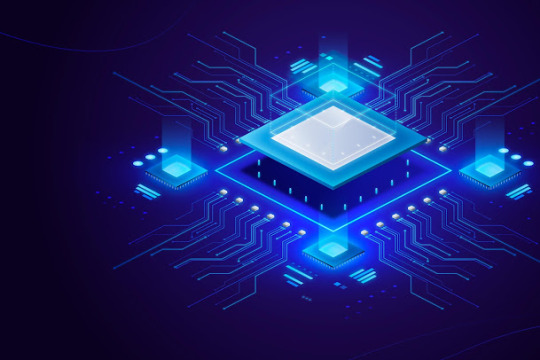
Understanding 3D IC Technology - An Overview | PCB Power
As the world demands faster, more powerful, and smaller devices, traditional chip designs are hitting their limits. That’s where 3D IC technology steps in. Instead of spreading circuits out flat, like in conventional 2D designs, 3D ICs stack layers of integrated circuits, opening up new possibilities for performance, power efficiency, and space-saving. Imagine more computing power packed into a smaller area with better communication between layers—that’s the promise of 3D ICs.
In this blog, we'll dive into how 3D IC technology works, the benefits it brings, and the hurdles we need to overcome as we look toward the future of electronics…
What is 3D IC Technology?
Over the past four decades, advancements in ASIC (Application-Specific Integrated Circuit) technology have drastically improved the power and efficiency of semiconductors. However, as we try to pack more power into devices, making chips larger has become increasingly difficult, expensive, and time-consuming. We're reaching the limits predicted by Moore’s Law, where doubling the number of transistors on a chip is no longer as easy or cost-effective as it used to be.
This challenge has led to the rise of 3D IC (Integrated Circuit) technology. A 3D IC is made up of two or more smaller chipsets—essentially mini integrated circuits—designed to work together within the same package. These chipsets are connected using advanced packaging methods, whether it's 2D, 2.5D, or fully stacked 3D techniques. Instead of relying on the traditional approach of cramming everything into a single layer, 3D ICs divide the workload across smaller, more manageable pieces that are either stacked on top of each other or connected side by side. This not only reduces the overall size of the chip but also dramatically boosts performance without needing to duplicate components.
By embracing 3D IC technology, we can keep pushing the boundaries of semiconductor innovation, even as traditional methods reach their limits.
Benefits of 3D-IC Technology
The benefits of 3D-IC Technology are as follows:
Low Expenditures: Components such as analog circuits and memory can be fabricated on older generations of technology without additional cost.
Enhanced Capability: Boosted speed and bandwidth support up to 100 Gbps in advanced memory applications.
Space Efficiency: Miniature 3D ICs are used on smaller boards. It is useful for compact mobile devices.
Less Wasted Energy: Provided smaller I/O drivers and fewer RLC parasitics cause better efficiency in power consumption.
Faster Time-to-Market: Modular design and possibilities of “die reuse” accelerate project development.
Increased Integration: Allows one system to implement photonics, MEMS, and other new technologies.
Enhanced Signal Integrity: The use of TSVs lowers parasitics, which leads to better performance and saves power much better than traditional SiP designs.
Flexibility: Different technological nodes of dies can be stacked, making the system design more versatile.
3D ICs have a denser configuration, quicker interconnects, and better power characteristics; therefore they revolutionize the concept of high-performance applications, through design, heat control, and ramp-up production.
Applications of 3D IC Technology
3D IC technology is transforming industries that require high-performance and compact designs. Its ability to stack layers of circuits has made it an essential component in advanced computing, AI, and data centers, where speed and efficiency are critical.
It’s also revolutionizing the smartphone and wearable tech markets, enabling thinner devices with more power. In automotive applications, 3D ICs contribute to smarter, faster processing for autonomous driving systems. Additionally, 3D ICs are increasingly used in healthcare devices, powering sophisticated imaging and diagnostic equipment that rely on speed and accuracy.
Challenges in 3D IC Technology
Setbacks experienced with 3D IC Technology:
Heat Management: Ever-rising vertical stacks create a high level of power density and hence create thermal hot spots which may negatively affect performance and reliability. Also, adequate control of heat flow between the layers is necessary to avoid thermal crossover which may lead to defects in the circuitry.
Manufacturing Difficulty: The extent of tolerances required for the alignment and bonding of the dies in 3D IC exceeds that of 2D IC resulting in greater manufacturing costs and time as well as problems in increasing production volume.
Design Validation: The features of a 3D IC make design validation processes very difficult. Existing methods are ineffective due to the complexity of multilayer interactions and new ones need to be developed.
Differential Thermal Expansion Ratios: Materials with differing thermal expansion coefficients can result in mechanical stresses that lead to distortion and failure. Therefore appropriate materials and designs should be employed to avoid such occurrences.
Electromagnetic and power management problems: The performance of power-integrated circuits with multiple layers may be limited because of the complex power distribution within the stacked layers. Designers would require high-end software to model power distribution and temperature effects precisely to ensure the systems work well.
The Future of 3D IC Technology & PCB Power's Role in Driving Innovation
3D IC technology is shaping the future of electronics, bringing forth smaller, faster, and more energy-efficient devices. With its ability to stack circuits vertically, 3D ICs significantly reduce signal delays and improve overall performance, making them key to advancing AI, IoT, and other emerging technologies.
However, the journey to full adoption is not without challenges. Thermal management, manufacturing complexity, and the need for reliable interconnects are crucial hurdles that the industry needs to address. This is where PCB Power steps in.
At PCB Power, we understand that as IC designs become more sophisticated, the demand for high-performance PCBs will only grow. Our expertise in creating multi-layer and high-density interconnect (HDI) PCBs ensures that we can meet the evolving needs of 3D IC technology. We continuously adapt our processes to support cutting-edge designs and ensure that signal integrity and heat dissipation are prioritized.
Whether you’re looking for custom PCBs for advanced 3D IC applications or turnkey solutions that streamline the PCB manufacturing and assembly process, we are here to partner with you every step of the way.
As we look to the future, PCB Power remains committed to pushing the boundaries of PCB technology, helping businesses like yours thrive in this exciting era of innovation.
Read the original blog post here: Understanding 3D IC Technology - An Overview
0 notes
Text
https://www.futureelectronics.com/p/interconnect--connector-tools-contacts-accessories/0462-005-20141-te-connectivity-3076065
What is a cable assembly, crimping tool, electrical connector, Crimp tools,
16-18 AWG Size 20 Nickel Plated Crimp Automotive Terminal Contact Socket
#Connectors#Tooling and Accessories#0462-005-20141#TE Connectivity#What is a cable assembly#crimping tool#electrical#circular#USB#PCB#rectangular industrial#SMA RF#Barrier strip#data connector#transmitting power#Wire crimp#socket
1 note
·
View note
Text
Unveiling PCB Assembly Cables: Bridging the Gap in Electronic Design

In the world of electronics, the assembly of Printed Circuit Boards (PCBs) is a complex process that requires precise attention to detail. One crucial aspect often overlooked in the PCB assembly process is the role of PCB assembly cables. These cables are vital for connecting and integrating different electronic components and systems, ensuring that your devices operate efficiently and reliably. If you’re curious about PCB assembly cables and their significance, this blog post will provide a comprehensive overview, including their types, applications, and considerations for choosing the right cables for your project.
What are PCB Assembly Cables?
PCB assembly cables, often referred to as cable assemblies or wire harnesses, are integral to the interconnection of various components within an electronic device. These cables facilitate communication and power transfer between PCBs and other system elements, such as sensors, connectors, and displays. They are designed to ensure that electronic systems function as intended by providing reliable and efficient connections.
Key Functions of PCB Assembly Cables:
Signal Transmission: PCB assembly cable carry electrical signals between different parts of a system, ensuring accurate data transfer and communication.
Power Distribution: These cables deliver power from the power supply to various components, maintaining the required voltage and current levels.
Mechanical Support: By securing connections and reducing stress on PCB connectors, assembly cables help prevent damage and ensure durability.
Types of PCB Assembly Cables
There are several types of PCB assembly cables, each suited to different applications and requirements. Here’s a look at some common types:
Flat Ribbon Cables:
Description: These cables consist of multiple wires arranged parallel to each other and encased in a flat, flexible insulation.
Applications: Often used in applications where space is limited and a large number of connections are needed, such as in computer motherboards and internal devices.
Round Cables:
Description: These cables feature a round cross-section and can include multiple wires insulated individually or as a bundle.
Applications: Common in power distribution and general-purpose connections where flexibility and durability are required.
Flexible Flat Cables (FFC):
Description: FFCs are thin, flexible cables that consist of flat conductors and are ideal for space-constrained applications.
Applications: Frequently used in compact electronic devices such as smartphones, cameras, and portable electronics.
Coaxial Cables:
Description: Coaxial cables have a central conductor surrounded by an insulating layer and an outer conductive shield.
Applications: Used for high-frequency signal transmission, such as in RF applications, video signals, and data communication.
Custom Cable Assemblies:
Description: Custom cables are designed and manufactured according to specific requirements and specifications provided by the client.
Applications: Ideal for specialized applications where off-the-shelf solutions are not suitable.
Applications of PCB Assembly Cables
PCB assembly cables find applications across a wide range of industries and devices. Some common areas include:
Consumer Electronics:
Devices: Smartphones, tablets, laptops, and gaming consoles.
Role: Connect internal components like displays, processors, and batteries.
Automotive Industry:
Devices: In-vehicle infotainment systems, engine control units, and sensors.
Role: Facilitate communication and power distribution within vehicle electronics.
Medical Devices:
Devices: Diagnostic equipment, patient monitoring systems, and imaging devices.
Role: Ensure reliable connections for data transfer and power supply in critical medical applications.
Industrial Equipment:
Devices: Manufacturing machinery, robotics, and control systems.
Role: Provide robust and durable connections to withstand harsh operating conditions.
Telecommunications:
Devices: Networking equipment, routers, and signal processors.
Role: Enable high-speed data transmission and connectivity.
Choosing the Right PCB Assembly Cable

Selecting the appropriate PCB assembly cable is essential for ensuring the reliability and performance of your electronic devices. Here are some factors to consider:
Application Requirements:
Considerations: Determine the specific requirements of your application, such as signal type, power needs, and environmental conditions.
Cable Specifications:
Factors: Evaluate cable specifications including gauge, insulation type, shielding, and flexibility based on your design requirements.
Durability and Reliability:
Assessment: Ensure the cables are durable and reliable, particularly in harsh environments or critical applications.
Custom vs. Standard Solutions:
Decision: Decide whether off-the-shelf cables are sufficient or if custom solutions are needed to meet specific design constraints.
Quality and Compliance:
Standards: Choose cables that meet industry standards and certifications to ensure MT PCB Assembly quality and compliance.
PCB assembly cables are crucial components in the electronic design and assembly process, playing a vital role in connecting various parts of a system and ensuring seamless operation. Understanding the different types of cables, their applications, and the factors to consider when selecting them can significantly impact the performance and reliability of your electronic devices.
By focusing on quality and choosing the right cables for your specific needs, you can ensure that your PCB assemblies operate efficiently and effectively, paving the way for successful and reliable electronic products.Pcb Assembly Cable
#Pcb Assembly Cable#4 Cores Power Cable#4pin Connector Cable#5pin Connector Cable#MT PCB Assembly#printed circuit assembly#pcba circuit board
0 notes
Text

PCB of the day! Requiem for a 5.1K CC resistor 🔌💡🔧
We have a few gadgets around the house that, despite having a USB type C connector, do not abide by the USB C power delivery specification! They leave off or mis-connect the two 5.1K resistors required to tell a USB PD wall adapter that they want 5V 1A power, a common issue because the devices work fine with a USB A to C cable, and only Macbooks seem picky about this stuff: cheap power supplies blast 5V and call it a day. This doo-hickey is a solution. It has two USB sockets nestled back-to-back, and instead of connecting the CC lines through, each half has its own dedicated resistor set. It makes for an excellent symmetrical design. Pair it with a short USB C-C cable to create an inline extender. We considered having one side be a plug, but the SMT-able plug connectors seemed like they needed to be more mechanically stable.
#adafruit#electronics#pcb#opensource#opensourcehardware#pcboftheday#usb#usbc#resistors#power#gadgetfix#techsolution#macbookissues#usbpd#powerspecs#circuitdesign#techhack#hardwaremods#diyelectronics#gadgethack
15 notes
·
View notes
Text
https://www.futureelectronics.com/p/semiconductors--optoelectronics--leds/sml-lx0404siupgusb-lumex-5003908
PCB Surface Mount LED, High Power Optoelectronics, Led display screen,
Red/Green/Blue 0404 120° Water Clear 30/40/20 mcd PCB Surface Mount LED
#Optoelectronics#LEDs#SML-LX0404SIUPGUSB#Lumex#Isolation components#Light emitting diode#Light-emitting diode#laser led#PCB Surface Mount LED#High Power#Led display screen#Programmable led display
1 note
·
View note
Text
Star product: A solid fortress guarding smart water meters—YMIN 3.8V supercapacitor
Market Prospects for Smart Water Meters

Smart water meters are in high demand due to urbanization, improved living standards, and environmental awareness. The market is growing, especially with the upgrade of water supply facilities and new residential projects.
YMIN 3.8V Supercapacitor Function
YMIN 3.8V supercapacitors, paired with lithium-thionyl chloride batteries, ensure smart water meters perform data storage, measurements, and remote communication efficiently by providing high-power output and preventing battery passivation.

Advantages
Low Temperature Resistance: Operates stably from -40°C to +70°C.
Long Lifespan: Reduces maintenance costs due to non-chemical reaction energy storage.
Ultra-Low Self-Discharge: Minimizes static power consumption.
Maintenance-Free: Combines with batteries for optimal performance.
Conclusion
YMIN 3.8V supercapacitors offer reliable, long-lasting energy solutions for smart water meters, ensuring stable operation in various environments.
#smarthome#smartmeter#meter#electricmeter#Electronic equipment#capacitors#electronic#power management#PCB design#games#critical role
0 notes
Text
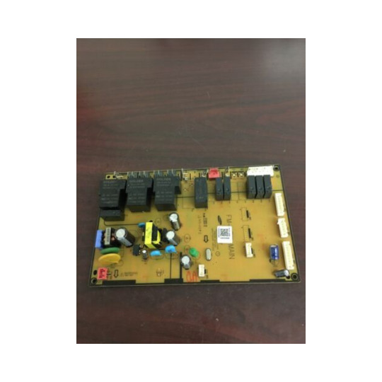
Samsung DG92-01084A Range Pcb-Main | HnK Parts
#DG92-01084A#Samsung#Range#PcbMain#HnKParts#KitchenAppliance#HomeAppliance#Manufacturer Name:Samsung#Product Number:DG92-01084A#OEM Part Number:DG92-01084A#The Samsung DG92-01084A is a vital component for Samsung ranges#functioning as the main printed circuit board. Consider it as your range's intellect#which includes critical electronic parts which regulate multiple operations. A properly working PCB makes sure your range works smoothly#including regulating temperature settings to offering quick buttons and a comprehensive power supply.#https://www.hnkparts.com/dg92-01084a-smg-pcb-main
0 notes
Text

Letting you focus on design and marketing, we specialize in handling your procurement and manufacturing processes.Submit Your Gerber and BOM Files for a Free Fab/Assembly Quote!
#pcb#pcba#pcblayout#pcbfabrication#pcbdesign#pcbassembly#SMT#DIP#BGA#electronics#component#USB#ledboard#aluminum#pcbboard#IC#power#supply#Bluetooth#HDI#sports#headset
0 notes
Text
What is Heavy Copper PCB or Thick Copper PCB?
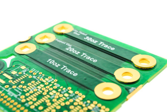
In high-power applications, managing ultra-high thermal loads and high-power currents is crucial. Standard PCBs typically have copper thicknesses ranging from 1oz to 3oz. However, in scenarios requiring robust current management and thermal dissipation, Heavy Copper PCBs, also known as Thick Copper PCBs, come into play. These boards have finished copper weights between 4oz and 10oz, with some super thick copper PCBs reaching 20oz to 200oz per square foot. The increased copper thickness enables these PCBs to handle high current outputs and optimize thermal management, crucial for electronics applications where temperature control is paramount to avoid performance degradation and premature failure.
Additionally, thick copper layers allow for large PCB cross-sections, which are ideal for high current loads, and facilitate heat dissipation. These PCBs also enable the integration of finely laid out structures on the outer layers with thick copper layers on the inner layers, providing a versatile solution for various design requirements.
Construction of Heavy Copper PCB
Manufacturing thick copper PCBs involves a combination of etching and electroplating processes, similar to standard PCBs. However, special techniques are required to ensure that trace sidewalls and undercuts meet the standards for thick copper features. Some of the main challenges in manufacturing thick copper PCBs include the need to remove a significant amount of copper during etching, increased etching costs, and the difficulty in manufacturing thin traces and ensuring the evenness of thick traces.
How to Make Thick Copper PCB?
The manufacturing process for thick copper PCBs involves several key steps to ensure the even thickness of the copper layers. These steps include etching inner layer traces on each layer of the inner core material, designing pads with uniform spacing and positioning, and using appropriate methods for burying copper in the prepreg. Common processes for thick copper PCBs include inserting thick copper bars into the circuit board, using laminate deposition with a thick base copper, and burying copper in the prepreg using laser cutting.
Advantages of Heavy Copper PCBs
Heavy Copper PCBs offer several advantages over standard PCBs:
Excellent high heat resistance: Heavy Copper PCBs can withstand high temperatures, making them ideal for high-power applications.
Improved current carrying capacity: The increased copper thickness allows Heavy Copper PCBs to carry larger currents with the same line width.
Reduced complex wiring: Heavy Copper PCBs can simplify complex wiring configurations, leading to more efficient designs.
Compression of board size: Heavy Copper PCBs allow for the integration of multiple copper weights on the same PCB, reducing the overall size of the end-use product.
Enhanced mechanical strength: The use of thick copper in PCBs improves the mechanical strength of the board, particularly in areas such as PCB connector areas and plated through holes (PTH).
Improved thermal management: Heavy Copper PCBs facilitate better heat dissipation, which is crucial for maintaining the performance and longevity of electronic components.
Ordinary PCB vs. Heavy Copper PCB
The main differences between standard PCBs and Heavy Copper PCBs lie in the manufacturing process and the copper weight. Standard PCBs are made through processes such as etching, hole drilling, and electroplating, while Heavy Copper PCBs require finer differential pair etching and step plating processes to ensure trace quality. Additionally, the copper content per square foot of a standard PCB is between 1oz and 3oz, whereas for Heavy Copper PCBs, the copper content exceeds 3oz.
Difference between Copper PCB and Heavy Copper PCB
Copper PCBs and Heavy Copper PCBs serve different purposes, with the main distinction being the thickness of the copper foil. Copper PCBs refer to PCBs with a copper substrate, which helps dissipate heat and prolong the life of components. On the other hand, Heavy Copper PCBs have a copper thickness exceeding 3oz and are used for their high current-carrying capacity.
Characteristics of Heavy Copper PCBs
Heavy Copper PCBs offer several unique features:
Ultra-high mechanical strength: Thick copper layers enhance the mechanical strength of the PCB, making it more resistant to weather and external stresses.
Excellent weather resistance: Heavy Copper PCBs can withstand extreme temperatures and harsh environmental conditions, ensuring the stability of the circuit transmission signal.
Thermal management: Thick copper layers improve heat dissipation, crucial for modern, high-density PCBs with high current loads.
Excellent current conduction: Heavy Copper PCBs provide excellent conductivity, facilitating the transmission of electricity between various components.
Diversity: Heavy Copper PCBs support various conductive and substrate materials, production processes, and application fields, making them versatile for different design requirements.
In conclusion, Heavy Copper PCBs play a crucial role in high-power applications where robust current management and thermal dissipation are essential. Their unique construction and characteristics make them ideal for applications requiring high heat resistance, excellent current carrying capacity, and improved thermal management.
High quality PCB manufacturer from China
0 notes