#PCB-Driven Mechanical Modeling
Explore tagged Tumblr posts
Visit Tumblr Blog
Explore Tumblr blogs with no restrictions, modern design and the best experience.
Last Seen Tumblr Blogs


Fun Fact
Hackers stole 65M passwords from Tumblr in 2013.
Text
Minimize Design Iterations with PCB-Driven Mechanical Modeling
When it comes to product development, one thing’s clear—every iteration costs time. And in today’s fast-moving market, time is everything. That’s where PCB-driven mechanical modeling steps in to smooth out the bumps before they become costly detours.
This approach doesn’t just reduce revisions—it helps teams design smarter from day one. If you’re looking to tighten workflows and avoid unnecessary back-and-forth, this might just be your new favorite strategy.
Let’s break it down.
🚀 What Is PCB-Driven Mechanical Modeling?

In simple terms, it’s the integration of your Printed Circuit Board (PCB) layout into the mechanical CAD environment—early and accurately.
Instead of designing the enclosure and board in silos, the two are brought together right from the start. That means fewer surprises later.
No more, “Oh no, the USB port doesn’t line up,” or “Wait, there’s interference with that component.”
This is especially important in Mechanical & Thermal Design, where space, airflow, and structure must work in harmony with the electronics.
🧩 Why It Reduces Iterations
Traditional workflows often mean:
The electrical team finishes the PCB layout
The mechanical team gets it later
Changes and corrections begin...
Sound familiar?
With PCB-driven modeling, mechanical constraints like fit, clearance, airflow, and mounting can be addressed as the board is being laid out. You’re not designing in the dark.
In short, you:
Catch conflicts early
Avoid rework
Save valuable time
This keeps the Mechanical & Thermal Design process efficient, collaborative, and focused on results.
🛠️ Key Benefits of This Approach
1. Better Fitment, Fewer Surprises
All parts—screws, standoffs, connectors—can be placed with confidence. No last-minute enclosure redesigns.
2. Improved Thermal Planning
Heat-generating components can be positioned for optimal airflow and cooling solutions can be integrated without guesswork. That’s a big win for any Mechanical & Thermal Design process.
3. Streamlined Collaboration
Designers and engineers speak the same visual language when everything is modeled together.
4. Faster Time to Prototype
Less rework means quicker decisions, which leads to faster prototyping and testing.
🔄 Real-World Application: How It Fits Into the Workflow
Here’s how it usually plays out:
PCB layout starts with basic mechanical guidelines.
Mechanical model imports that layout and applies accurate dimensions, hole placements, and component heights.
Design teams collaborate in real-time to optimize the enclosure and internal spacing.
Thermal and structural simulations can now be run on a near-final assembly—before the first prototype is even made.
That tight loop is where the magic happens. It gives the Mechanical & Thermal Design process clarity and confidence.
🌬️ Don’t Forget Thermal
PCB-driven modeling also sets the stage for thermal analysis.
When component locations are fixed early, it’s easier to simulate heat flow and explore solutions like:
Heatsinks
Thermal pads
Air vents
Fans
This proactive mindset is what separates smooth launches from frustrating delays.
And yes, it’s a big part of modern Mechanical & Thermal Design strategies.
👀 Scannable Summary
What it is: Real-time mechanical modeling using actual PCB layout data
Why it matters: Reduces design iterations, errors, and rework
Top benefits: Better fit, faster prototyping, smarter thermal planning
Big picture: Aligns electrical and mechanical teams early in the process
Key use: Enhancing overall Mechanical & Thermal Design efficiency
✨ Final Thoughts
PCB-driven mechanical modeling isn’t just another box to tick—it’s a smarter way to work. When mechanical and electrical design speak the same language from day one, everything flows smoother.
And in a world where every iteration counts, that kind of alignment makes all the difference.
Whether you're designing a wearable, a power device, or an embedded system, this approach keeps your Mechanical & Thermal Design process on track—and your headaches to a minimum.
❓FAQs
Q1: Is PCB-driven modeling only useful for complex products?
Not at all. Even small devices benefit from early mechanical integration, especially when space is limited or thermal performance matters.
Q2: Does this replace traditional design methods?
No, it enhances them. It complements standard workflows by reducing manual back-and-forth and aligning teams earlier in the cycle.
Q3: What tools are typically used?
Mechanical CAD tools that support PCB import or integration, as well as simulation tools used in Mechanical & Thermal Design, are commonly used. The key is compatibility and collaboration.
0 notes
Text
Why Should You Rely on Connector Wrenches for Precision and Safety?

Introduction to Connector Wrenches
Connector wrenches are essential tools engineered to simplify the tightening and loosening of connectors in a wide variety of electrical, electronic, and mechanical assemblies. Unlike generic wrenches, connector wrenches are specially designed to provide optimal torque control, ensuring secure connections without damaging delicate components. Their role is increasingly important in precision-driven industries, from telecommunications and aerospace to electronics manufacturing and data centers. The compact design and compatibility with hard-to-reach spaces make these tools a must-have for technicians and engineers working with connectors, sensors, cables, microcontrollers, and other sensitive components.
Why Are Connector Wrenches So Important?
Connector wrenches serve as the interface between quality installation and long-lasting performance. Whether assembling fiber optic cables or tightening RF connectors in communication equipment, these wrenches ensure a perfect fit and torque consistency, reducing the risk of signal loss or component failure.
Their significance extends across multiple fields:
In electronics, they provide careful application of pressure, preserving internal components.
In safety-critical environments, they prevent under-tightening or over-tightening, which can compromise functionality.
In thermal and high-frequency environments, they help maintain signal integrity and reduce potential system malfunctions.
With the rise in automated systems, robotics, and microelectronic devices, connector wrenches have become more refined, precise, and essential.
What Are the Key Features of a Connector Wrench?
Connector wrenches are built with attention to detail, functionality, and durability. The best models are manufactured using high-grade materials like stainless steel or anodized aluminum, and are compatible with various connector types and industry standards.
Key features include:
Ergonomic handles that provide a comfortable, anti-slip grip during repetitive tasks
Torque-limiting designs to prevent damage to sensitive terminals or threaded connectors
Slim or angled profiles to access connectors in tight or obstructed areas
Interchangeable heads to work with different connector sizes or standards
Non-magnetic materials to ensure safety in environments with magnetic-sensitive components like capacitors, sensors, and microprocessors
These design features make connector wrenches versatile for professionals working with thermal pads, controllers, contactors, and other high-performance equipment.
How Are Connector Wrenches Used in Industry?
Connector wrenches are utilized across several technical sectors where precise connectivity is essential. In telecommunications, for example, connector wrenches are commonly used to install coaxial or fiber connectors. In the aviation and aerospace industry, they’re instrumental in ensuring vibration-resistant terminations. In electronics, especially during PCB assembly or repair, connector wrenches help technicians maintain uniform pressure on connector housings, cable grips, and solderless terminals.
They are also integral in:
Automotive electronics installation and diagnostics
Sensor placement in industrial automation systems
Power connector setup in energy distribution equipment
Secure mounting of thermal systems involving heatsinks or fans
Connector wrenches not only streamline workflows but also improve the longevity and safety of complex systems.
What Types of Connector Wrenches Are Available?
There is a wide range of connector wrenches, each tailored for specific applications or connector types. Selecting the right wrench ensures compatibility and precision.
Common types include:
Fixed-head connector wrenches for specific connector sizes and types
Adjustable connector wrenches for handling multiple dimensions with one tool
Torque-limiting connector wrenches with calibrated mechanisms for consistent tightness
T-handle and L-handle styles that enhance torque application in confined spaces
Ratcheting connector wrenches for high-efficiency repetitive tasks
Insulated connector wrenches designed for working with electrical connectors in live circuits
Selecting the correct type ensures compatibility with connectors in tools, switches, safety modules, microcontrollers, and more.
Where Are Connector Wrenches Most Commonly Applied?
Connector wrenches are ubiquitous in various high-tech and industrial environments. Their ability to handle components without risking deformation makes them especially useful in sensitive electrical and data systems.
Typical applications include:
Networking installations involving coaxial, SMA, or fiber connectors
Aerospace electronic equipment where vibration-resistant assembly is vital
Medical devices requiring delicate yet firm connection fittings
Industrial automation systems incorporating sensors, thermal components, and fuses
Consumer electronics involving microprocessors, LEDs, and compact controllers
Renewable energy systems for secure connection of high-power terminals and capacitors
These tools are ideal for use during both installation and maintenance phases.
What Are the Benefits of Using the Right Connector Wrench?
Using the right connector wrench can enhance performance, increase safety, and reduce rework. As systems become increasingly compact and complex, the precision offered by connector wrenches becomes even more valuable.
Key benefits include:
Enhanced reliability of electrical and mechanical connections
Minimization of torque-related connector damage
Efficient installation and maintenance of components such as switches, thermal pads, and cables
Reduction in installation time and human error
Compliance with technical standards in regulated industries
The result is a cleaner, more stable connection with increased system performance and reduced maintenance costs.
How to Choose the Ideal Connector Wrench?
Choosing the right connector wrench depends on various factors such as the type of connector, environment, access space, and required torque.
Consider the following criteria:
Material durability and resistance to wear
Ergonomic design suited for extended use
Compatibility with specific connector types (e.g., SMA, N-Type, DIN)
Availability of torque control if precision is critical
Magnetic safety when working near microelectronics
Size and weight for ease of transport in fieldwork
Investing in a quality wrench tailored to your workflow can make all the difference in precision and efficiency.
Final Thoughts
Connector wrenches play a vital role in ensuring reliable, secure, and professional-grade connectivity across electronics, automation, communications, and industrial applications. As the demand for high-performance systems increases, the importance of using precise tools like connector wrenches becomes evident. These tools enhance system performance, improve safety, and prolong the lifespan of critical components.
Whether you're an electronics technician working with sensors and microcontrollers or an engineer installing power connectors and thermal solutions, connector wrenches are your trusted companion for clean, secure, and efficient assembly. Explore quality options from trusted brands and elevate your toolkit for modern-day applications.
0 notes
Text
PTC Creo 12: New Tools for Smarter, Faster 3D Design
Discover what’s new in PTC Creo 12 — enhanced simulation, AI-driven design, MBD, and manufacturing tools. Upgrade now with ANH, the trusted PTC Creo reseller in the Delhi NCR region.
Top New Features in Creo 12
1. AI-Driven Design Guidance
Creo 12 takes intelligent design to the next level with built-in AI tools that offer real-time suggestions and improvements.
Get feedback during modeling
Reduce trial-and-error
Improve efficiency with every click
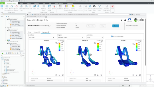
2. Enhanced Model-Based Definition (MBD)
Creo 12 makes MBD more practical and powerful, eliminating the need for traditional 2D drawings.
Improved PMI (Product Manufacturing Information)
Better GD&T annotation support
Clearer data for downstream users

3. Performance & Usability Upgrades
PTC has improved the overall speed, responsiveness, and ease of use:
Faster model regeneration
Smart mini toolbars
Enhanced model tree filters
Customizable dashboards for quick access

4. Creo Simulation Live — More Powerful Than Ever
Simulation Live has been expanded to cover:
Structural & thermal simulations
Better support for nonlinear materials
Real-time design feedback

5. Advanced Multi-Body Design
Creo 12 makes it easier to work with complex parts and assemblies:
Better control over multiple bodies in a single part
New body operations and organization tools
Improved part-to-part interactions
It’s ideal for high-detail engineering and intricate product development.
6. Additive and Subtractive Manufacturing Enhancements
Manufacturing has never been smoother in Creo:
More control over lattice structures
Enhanced 5-axis CAM functionality
New machine support and output formats
Whether you’re 3D printing or using CNC, Creo 12 has you covered.
7. Improved ECAD–MCAD Collaboration
With electronics becoming a bigger part of mechanical products, Creo 12 improves:
PCB visualization
Layer management
Synchronization between electrical and mechanical teams
This helps avoid costly errors during development.
Why Creo 12 is a Must-Have Upgrade
PTC Creo 12 isn’t just for big enterprises — it’s built for everyone who values smart, high-quality design. Whether you’re a design engineer, manager, or product innovator, Creo 12:
Saves time
Reduces errors
Encourages innovation
Supports industry 4.0 goals
Get Creo 12 from Delhi NCR’s Trusted PTC Reseller — ANH
Looking to upgrade your CAD tools or switch to Creo 12? ANH is a leading authorized PTC reseller in the Delhi NCR region. From licensing to training, we help businesses unlock the full potential of Creo.
Contact ANH today to get started with Creo 12!
✅ Conclusion: Welcome to the Future of Design
PTC Creo 12 is more than just an upgrade — it’s a gateway to smarter design, quicker development, and stronger innovation. With new AI tools, advanced simulations, and seamless usability, it’s built to give your team a competitive edge.
Design faster. Design smarter with Creo 12.
0 notes
Text
Printed Circuit Board Market Drivers: Key Forces Powering Global Electronics Manufacturing Growth
The printed circuit board market is experiencing sustained growth, driven by several powerful forces that reflect rapid technological advancement and industrial transformation. As the core component in nearly all electronic devices, PCBs are indispensable in industries ranging from consumer electronics to automotive, aerospace, and telecommunications. These boards provide the physical foundation for electronic components and circuitry, making their demand closely tied to innovation, manufacturing expansion, and digital integration across multiple sectors.

Rising Demand for Consumer Electronics
One of the most significant drivers of the printed circuit board market is the growing global appetite for consumer electronics. Devices such as smartphones, tablets, laptops, gaming consoles, and smartwatches rely heavily on compact and high-performance PCBs. As consumers increasingly seek devices that are faster, smarter, and more energy-efficient, manufacturers are pushing the limits of PCB design and complexity. The adoption of multi-layer and flexible PCBs has expanded to meet the needs of compact form factors without compromising performance.
Growth in Automotive Electronics
The automotive industry has emerged as a major contributor to PCB market growth. Modern vehicles are no longer just mechanical machines—they are smart systems powered by complex electronic architectures. From engine control units (ECUs) and infotainment systems to safety features like advanced driver-assistance systems (ADAS), automotive applications require highly durable and reliable PCBs. Furthermore, the rise of electric vehicles (EVs) and hybrid models has intensified the demand for power PCBs that can handle higher currents and extreme environmental conditions. As automakers continue to shift toward connected and autonomous driving technologies, the integration of sophisticated PCBs will only grow deeper.
Technological Advancements and Miniaturization
Ongoing innovations in PCB design and manufacturing techniques are another key market driver. Technologies such as surface mount technology (SMT), high-density interconnects (HDI), and embedded components have enabled the creation of smaller, more complex, and more efficient boards. These advancements allow PCBs to meet the growing needs of sectors like medical devices, wearable technology, and aerospace electronics. Miniaturization not only reduces device size but also enhances portability, a crucial factor in today’s fast-evolving digital world.
Expansion of the 5G Infrastructure
The global rollout of 5G infrastructure is propelling the demand for high-performance PCBs. 5G technology requires sophisticated network equipment, including base stations, routers, and antennas, all of which depend on advanced PCBs capable of supporting high-frequency signals. The need for increased data speeds, low latency, and massive device connectivity makes PCB innovation a critical part of the 5G ecosystem. Manufacturers are investing heavily in materials and designs that reduce signal loss and improve thermal performance to support 5G components.
Industrial Automation and IoT Adoption
Industries are rapidly embracing automation, artificial intelligence, and the Internet of Things (IoT), which directly contributes to increased PCB usage. In industrial settings, PCBs are used in sensors, control systems, robotics, and other automated machinery. The proliferation of smart devices and connected systems in manufacturing environments has amplified the requirement for reliable PCBs with enhanced connectivity features. Additionally, smart home systems, wearable health monitors, and connected appliances represent a fast-growing segment that depends on efficient PCB integration.
Environmental and Regulatory Push
Environmental regulations and the push toward sustainable electronics have influenced manufacturers to adopt eco-friendly PCB materials and cleaner production processes. Lead-free soldering, halogen-free laminates, and recyclable substrates are increasingly in demand. This shift toward sustainable solutions not only meets regulatory standards but also aligns with consumer expectations for greener technologies. As more companies adopt environmental certifications and green manufacturing methods, the printed circuit board market is seeing a transformation in both product development and supply chain management.
Strategic Investments and Supply Chain Expansion
The globalization of electronics manufacturing has led to the development of robust supply chains and strategic investments in PCB production facilities. Asia-Pacific, particularly China, South Korea, and Taiwan, continues to dominate PCB manufacturing, but other regions are rapidly expanding their capabilities to reduce dependence on single-region supply chains. Companies are also investing in smart factories, automation, and digital twin technology to enhance production efficiency and meet rising global demand.
Conclusion
The printed circuit board market is being driven by a convergence of technological innovation, industry-specific demands, and global infrastructure developments. From smartphones and electric vehicles to 5G networks and smart factories, PCBs remain the foundation of modern electronic systems. With ongoing advancements in design, materials, and functionality, and an ever-growing list of applications, the future of the PCB market looks robust and full of opportunity. As industries evolve, so too will the critical role of PCBs in powering that evolution.
0 notes
Text
Best CAD Drafting Software for 2025

Whether you're designing skyscrapers or prototyping parts for the next big innovation, CAD drafting tools are the backbone of modern engineering and architecture. As we head into 2025, the landscape of CAD software continues to evolve rapidly with smarter features, better integrations, and cloud-based workflows. If you're considering upgrading or just curious about what tools are leading the charge, here's our list of the top 10 CAD drafting tools you should absolutely know about in 2025.
If you offer or depend on CAD drafting services, this list is going to be especially relevant.
1. Autodesk AutoCAD
Still the reigning champion in many drafting departments, AutoCAD continues to deliver precision and performance. The 2025 version features enhanced automation, better collaboration tools, and AI-driven commands that reduce repetitive tasks. With robust DWG file support and integration with cloud services like Autodesk Docs, it's still a go-to for 2D drafting.
2. SolidWorks
Especially popular in mechanical design, SolidWorks remains a strong player. Its 2025 update brings deeper integration with Dassault Systèmes' 3DEXPERIENCE platform, improved simulation capabilities, and real-time collaboration features. It's ideal for product development and prototyping.
3. Autodesk Fusion
Fusion is quickly becoming a favorite thanks to its all-in-one platform combining CAD, CAM, CAE, and PCB tools. The 2025 version introduces AI-assisted modeling, generative design improvements, and expanded manufacturing features. It's cloud-native, so it's great for remote teams.
4. BricsCAD
BricsCAD offers an affordable alternative to AutoCAD with similar DWG compatibility and a flexible licensing model. The 2025 edition has focused on AI-assisted drafting and machine learning to speed up drawing creation. Its ability to bridge 2D and 3D workflows makes it a solid contender.
5. SketchUp Pro
Originally loved by architects for quick 3D concept modeling, SketchUp Pro is now evolving into a full drafting and documentation tool. In 2025, it offers enhanced BIM capabilities, a sleeker interface, and improved LayOut integration for 2D documentation. Great for conceptual design and early-stage development.
6. DraftSight
DraftSight, developed by Dassault Systèmes, is another strong alternative to AutoCAD. The 2025 version boasts better 3D modeling capabilities and smoother DWG compatibility. It’s perfect for those who want professional-grade tools without the Autodesk price tag.
7. TinkerCAD
While it may seem basic compared to others, TinkerCAD has carved out a niche in education and rapid prototyping. The 2025 updates make it even easier to 3D print and simulate designs, making it a top choice for beginners or quick project ideation.
8. Rhino 3D
Rhino 3D continues to shine in industries like architecture, jewelry, and product design, thanks to its freeform modeling capabilities. The latest version enhances Grasshopper (its visual scripting tool) and supports even more plugins. Rhino's flexibility makes it a favorite for bespoke and complex modeling.
9. Onshape
Fully cloud-based, Onshape is revolutionizing collaborative CAD work. In 2025, it's leading the way in version control, browser-based modeling, and team-friendly tools. Onshape is excellent for product design firms and startups looking for scalability and remote-friendly workflows.
10. FreeCAD
For open-source enthusiasts, FreeCAD is getting more powerful with every release. The 2025 version has improved parametric modeling, a better GUI, and stronger support for industry-standard formats. It's ideal for those who want a cost-free yet capable solution.
How ProtoTech Solutions Helps
Staying ahead in CAD drafting is not just about the tools—it's about how you use them. That’s where ProtoTech Solutions steps in. With years of expertise in developing custom plugins, CAD automation tools, and providing tailored CAD drafting services, ProtoTech helps businesses get the most out of their software investments.
Whether you're looking to streamline your design workflows, create bespoke CAD tools, or outsource complex drafting tasks, ProtoTech can help you stay competitive in 2025 and beyond. Our team is fluent in all major platforms and can adapt to your unique project requirements.
The world of CAD drafting tools is more dynamic than ever. With AI, cloud computing, and collaborative tools reshaping workflows, it's essential to stay updated with what each platform offers. No matter which tool you pick from this list, pairing it with the right expertise and support, like what ProtoTech Solutions provides, can make all the difference.
Ready to level up your drafting game? Let ProtoTech Solutions be your CAD partner in innovation.
#CAD Drafting Tools for 2025#CAD Drafting Tools 2025#CAD Tools 2025#CAD Design#CAD Drafting#cad drafting services#outsource cad drafting services#cad outsourcing services#cad drafting outsourcing#outsource cad services#outsource drafting services#cad drafting outsourcing services#cad outsourcing#cad drafting company#cad outsourcing companies
0 notes
Text
Electronic Dosing Pump: Working and Set up
Electronic diaphragm dosing pumps, also known as solenoid pumps are controlled electronically by a PCB and are solenoid driven. These pumps are used to dispense or inject a precise amount of fluid into a process. They are most commonly used in water treatment applications such as in cooling towers, boilers, and industrial wastewater treatment.
Electronic dosing pumps are usually made from plastic, thermoplastic, or stainless steel and are attached to an electronic controller that enables the fluid flow to be monitored and adjusted easily. Among the various types of dosing pumps, electronic dosing pumps are preferred in many industries, especially for chemical feed applications due to their cost-effectiveness, ease of use, reliability, and high degree of accuracy. They are the core part of integrated metering systems and are designed for automatic chemical dispersion.
Electronic Dosing Pumps use expansion and contraction chambers to move the fluid. They can pump a variety of liquids including corrosives, acids, and bases as well as viscous liquids and slurries.
How does a dosing pump work?
Depending on the brand and model, a dosing pump functions in different ways. All these methods involve drawing a certain amount of liquid and injecting the chemical into the tank or pipe containing the fluid being metered. An electronic dosing pump is powered by an electric motor or air actuator and has a controller that turns the pump on and off while managing the flow rate as well.
Electronic dosing pumps are positive displacement pumps that use a reciprocating diaphragm to move the fluid. Since these pumps do not have any internal parts that can rub against each other to create friction and cause wear, they are quite reliable and have a long life. In addition to this, they also do not require seals or lubrication in the pump head, which also negates the possibility of oil vapor contamination or leakage of the pumped medium.
The key parts of electronic dosing pumps in India are a diaphragm, two valves, a displacement chamber, and a drive mechanism. The diaphragm is a flexible diaphragm that vibrates to create suction to move the fluid in and out of the pump chamber. It is located between the discharge chamber and the connection flange. The two valves operate by allowing fluid to move in and out of the chamber. They are usually baffle vales or spring-loaded ball valves made of the same material as the diaphragm.
When a dosing pump is primed, that is, all the air is pushed out of the lines up to the injector, then it is set for the required dose rate or set to work from its input signal. Once it starts operating, the pump works at its required flow rate until a stop signal pauses the action.
An electronic dosing pump is designed to be reliable so once it is set up properly, it does not require a lot of input except in emergency situations. If there is a product level problem or any other problem, an alarm activates to warn the operator. If the product runs out, the system may also shut down to avoid untreated water or liquid seeping into the treated fluid.
How to set up a dosing pump?
Since the components of a dosing system are very important, their setup is critical to its overall performance. The first thing to ensure is that all the components are compatible with the product being dosed and the feed stream. Fluids that are highly corrosive, have high pressure or high temperature needs specialized parts so that the dosing system does not melt, burst, or corrode. The best electronic dosing pump manufacturers in India provide their clients with consultancy services to determine what kind of electronic dosing pump would suit their needs the best.
Once you determine that everything is compatible, the next step is deciding an appropriate dosing point. There are two things that must be taken into consideration while determining this, the point should be located where the product mixes well and does not affect any other pipe parts. For example, if it is placed before a valve or water meter then these parts could prematurely corrode, not read properly or have a build-up of scale or sludge.
After the selection of a dosing point, the pump needs to be properly located. The ideal point is next to power or compressed air to make it work which is generally next to or below the dosing point to prevent siphoning and protect the water from dust, sun, or heat damage. Even though a dosing pump can handle extremely corrosive products, it is not weather resistant and their casing has a low IP rating so they need to be protected in a cabinet or housing to maximize working life.
Another factor that needs to be taken into consideration is the product container. This depends on the product being dosed, the quantity being dosed, and how much needs to be stored at the pump. If the pump is to be placed in a location that is hard to access or is going to be left for long periods of time, then a large amount of product needs to be stored. For this, a bulk tank or an IBC container can be used.
If all these things are taken into consideration then the system should work efficiently and safely. One of the crucial things with dosing systems is that you cannot cut corners with it as it can affect the efficiency of the whole system and the cost, safety and output will be compromised.
In this article, the working and installation of electronic dosing pumps are discussed. When you purchase electronic dosing pumps in India, it is crucial to select the right pump for your process. Electronic dosing pump manufacturers in India help in selecting the ideal pump for your process, maintain or overhaul the pump, and are always ready in case of emergencies to guarantee the continuity and smooth functioning of your process.
#electronic dosing pumps in India#electronic dosing pump manufacturers in India#electronic dosing pump
0 notes
Text
What are BGA PCB Soldering Joints
The underside of the chip pronounced. BGA PCB has many compared to wired IC advantages such as: • Smaller housing • Higher packing density • Higher pin density • Improved signal transmission properties • Better thermal coupling to the circuit board
Latest forms of these components, such as which enable VFBGA (Very Fine BGA) meanwhile several thousand connection pins with a pitch of less than 0.5mm. The BGA PCB components are assembled in a corresponding soldering process, with many factors play a role. The result of this process is usually a matt.
• High level of liability between the ball and circuit board • High mechanical long-term stability • The high structural integrity of the ball body • High conductivity • High electrical signal integrity • High insulation resistance to neighboring pins
At this point the interaction between the physical states and the resulting electrical properties clearly. The reference model shows the structural relationships in a simplified manner. It is based on a static, directional signal with simple ohmic. The conditions prevailing in the chip (bond wires, etc) are neglected as well known.
Static reference model between the mechanical and the electrical level during the soldering process, the solder of the balls melts with the solder paste and it forms a chemical reaction with the surface of the circuit board an intermetallic zone. Also, there is an intermetallic zone between the chip and the ball body, which, however, is pronounced at the chip manufacturer and must also be checked by him. This should normally be between the transmitter and the receiver should be stable at the milliohm level.
But all theory is gray because in practice both systematic and random occur errors and these lead to greatly changed electrical parameters and also one shiny solder joint is by no means a guarantee of freedom from errors. They range from visible deformations of the solder body in the senses of lean or fat solder joints, where there is electrical contact, up to optically well-defined solder joints with no, or sporadically falling electrical contact.
The standard IPC-A-610E plays an important role in the evaluation of a BGA PCB soldering joint role. It specifies the acceptance criteria for electronic assemblies and also specifies criteria for BGA PCB components. So for a production system solutions are necessary which ensure the conformity of the solder joints to this standard can demonstrate. This also causes structurally unstable solder joints where it is underneath mechanical stress to break and thus to loss of electrical conductivity comes avoided. However, it remains to be noted that many errors, the shape of the solder body regarding, only have electrical effects at extreme values.
Worth mentioning here are the "Head in Pillow" and "Black Pad “known phenomena. With the former effect, the solder does not melt with the solder paste and a quasi-barrier layer is formed. However, the optics of the solder joint reveal this typically not. The main causes, in this case, are contamination of the ball surface.
The problem with the black pad is more towards the circuit board. Here the reacts ball with the solder paste but below it also creates a layer with reduced or complete lack of conductivity.
Overview of typical error categories for BGA PCB soldering joints
However, they do lower resolution and thus problems in the detection of liability weaknesses in the intermetallic zones. AXOI devices combine AXI and AOI in one system
They are also capable of failing BGA PCB soldering joints on incorrectly placed chips due high-density BGA assemblies with conductor tracks completely embedded in the circuit board are pushing against it.
Put reliable methods like ICT and FPT aside for years. As groundbreaking the so-called boundary scan method, which is based on IEEE1149.x is standardized and works without an adapter. Starting from the discussed production requirements, crystallize for complex BGA assemblies focus on two technologies - X-ray systems in the form of AXI / AXOI and as an electrical test device boundary scan system. Both procedures are examined in more detail below.
Make full use of X-Ray's potential even if X-ray technology is basically able to use the BGA. Looking at balls is just a necessary technical basis. The actual customer benefit is primarily defined by technological device design.
X-ray systems are used in modern SMD production either directly in or next to the production line for fully automatic X-ray inspection (AXI) used. In summary, AXI systems for use in SMD production lines at BGA Assemblies meet a number of basic criteria, such as: • Complete inspection according to IPC-A-610E • Low slip • Low rate of ghost errors (false alarms) • Throughput in the area of the beat rate of the production line (in-line operation) • Automatic error detection • Simple program generation • Intuitive user guidance • Support for Statistic Process Control (SPC)
The IPC-A-610E addresses criteria such as those related to the BGA PCB components solder ball offset, solder ball distance, solder ball shape and pores (air pockets) in the soldering.
Particularly efficient to meet the requirements of the IPC-A-610 3D AXI systems based on tomosynthesis are to be checked, e.g. the OptiCon X-Line 3D from GÖPEL electronic.
OptiCon X-Line 3D with integrated AOI option (AXOI)

Well soldered BGA ball, Roundness OK Area OK Gray value OK

Badly soldered balls Roundness NOK Area NOK Gray value OK
Measurement of good and bad solder joints
The examples in Figure 3 show an example of a ball and its ball image processing evaluation. The pictures show the section through the middle of the BGA soldering balls. The example below shows that the amount of solder applied has an influence on void formation.
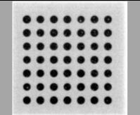
BGA - 50% solder volume, low voiding
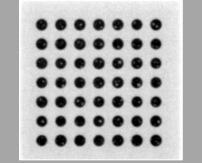
BGA - 100% solder volume, low voiding, light larger ball area
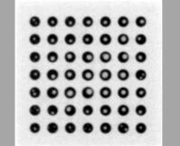
BGA - 200% solder volume, strong voiding recognizable
Representation of voids
Typically, the void test does not use the volume, but the void area certainly. Mainly the void area is related to the ball area and thus the void percentage issued.
The lower left example shows the automatic void determination. The IPC-A610E limit for the maximum proportion of void in the total solder joint is 25 percent.
Automatic determination of the proportion of void area to BGA area; Voiding = 27.4%; Measuring plane = ball center
Automatic determination of the proportion of void area to BGA area; Voiding = 27.4%; Measuring plane = ball center
Short circuits between two balls; these can also by means of an electrical test can be detected
Representation of void components, short circuits, and non-planar BGA
In addition to assessing the shape, presence, and pores of the solder balls, according to Figure 5 also short circuits between the solder balls are evaluated. If this BGA PCB is mechanically or thermally stressed, it will be expected to fail. Such an inclined position can include: stray components are caused that come to rest under the BGA. The error scenario of the "head-in-pillow" effect has already been discussed. It is also known under the synonym "trailer". One way of this failure scenario safely and to be able to test reproducibly is the use of a “tear-drop” pad design. in this connection, the connection pads of the BGA PCB are not circular, but tear-shaped.
X-ray image of a BGA with tear-drop design; the round pronounced soldering are trailers
X-ray image of a BGA with tear-drop design; the round pronounced soldering are trailers
Detection of trailers by tear-drop design
If a ball melts and combines with the solder paste underneath, it is shaped the typical teardrop shape. If no connection is established, the ball retains its circular shape and can be measured such as roundness, axis ratio or ball are abe sorted out.
The teardrop shape reduces the distance between two pads and it can cause injury of the minimum electrical insulation distance.
Now, a ball shape assessment is often not enough to make it bad differ. If there are assemblies on one side, you can use high-resolution 2.5D x-ray oblique radiation examined the transition between pad and solder ball become. If the constriction is recognizable here, this is an indication of a trailer.
ScopeLine MX-1000 for semi-automatic BGA analysis (MXI)
It’s better without needles This is a complementary partner for X-ray inspection of complex BGA assemblies Boundary scan procedure first choice.
This design-integrated test electronics is serialized via a so-called test bus driven. The virtual needles are actually boundary scan cells, which are in form a shift register (boundary scan register) can be interconnected. By the electrical test of BGA soldering joints succeeds in the synchronous handling of the problems of the cell. However, the fault location cannot be used for directional connections to be determined exactly, then processes such as MXI are required again.
Connection test of two BGA pins via boundary scan
With multi-point connections, e.g. Bus structures, on the other hand, is a pin accurate fault diagnosis completely given. But the charm of the boundary scan process is also its high test speed and flexibility when testing prototypes. Sophisticated system solutions such as the software platform SYSTEM CASCON ™ [6] from GÖPEL electronic offer automatic test pattern generators (ATPG) which thousands of test the solder joints in parallel in a few seconds and with automatic pin error diagnosis can, without the need for an adapter. It can hardly be more cost-effective. Boundary scan is a structural process and independent of that in the chip integrated functional logic. The bottom line is that each pin is individual and can be tested independently. This also makes the process very easy to use combine stress tests in which e.g. due to thermal stress in a climatic chamber attempts are made to cause defective solder joints to fail. It also offers for this GÖPEL electronic pre-assembled hardware modules, such as the TIC03 from the SCANFLEX series. But Boundary Scan also has its strengths in the laboratory. For quick prototype verification targeted check of certain signals is often relevant for the designer. Here graphic tools like Scan Vision ™ achieve the best results.
Representation of layout and schematic for interactive pin toggling
They not only allow cross-referencing between layout and schematic but also the activation of the boundary scan cells by simply clicking on the corresponding pin. The resulting logical signal states are then transferred from the user definable color schemes visualized. Special packages such as the PicoTAP Designer are also available for the introduction of Boundary Scan studio [8] from GÖPEL electronic available. They already contain all the tools including ATPG and debugger, as well as the necessary hardware to get started immediately. This also includes a hardware module for testing I / O signals. The special charm these packages are of course their extremely good price/performance ratio.
Components of the complete package PicoTAP Designer Studio
The very existence of the technologies and system solutions discussed so far is enough for one manufacturing with the highest quality standards is not enough. Rather, the use of X-ray systems and boundary scan systems in the production of BGA PCB assemblies a thorough analysis of the entire manufacturing situation. Above all, they play precise knowledge of the errors to be combated and their statistical distribution authoritative role. In total there are over 100 parameters that define an influence the optimal inspection and test strategy. In this respect, it is at this point impossible to name "the" strategy. But the fact is that the combination of AXOI and Boundary Scan at BGA provides 100 percent error coverage can guarantee and the greater the proportion of BGA is the more important precisely these techniques. From today's perspective, they are for high-density assemblies in perspective the only solution. What a process line looks like for such situations could be seen.
Example of using AXOI, MXI and Boundary Scan in a BGA PCB assembly line
The basic idea is to establish a sensor behind each process step and the statistical error information holistically on the processes fed back. The AXOI system can due to its high inspection speed qualify the module according to IPC-A-610E and, for example, also the inner meniscus measured by TQFP components. The still missing mechanical fault coverage is ensured by the integrated AOI system. MXI is used for precision analysis commitment. The sensors shown in blue are all in the GÖPEL product portfolio electronic included.
Summary and conclusions
BGA components are an important component of complex circuit boards and enable ever higher integration densities and improvements in the electrical parameters. The continuously decreasing access makes the use more appropriate countermeasures in the form of alternative inspection and test procedures are essential. In practice, 3D-AXOI machines, in particular, have a combined AXI / AOI system and Boundary Scan as the electrical test method for the greatest potential Solve the access problems. Both methods complement each other perfectly enable fault coverage against 100% for BGA soldering joints. It also offers boundary-scan fundamental future security as it progresses on standardization within the framework of the IEEE. That from GÖPEL electronic the developed concept of embedded system access (ESA) involves these standards and complements them with further technologies to extend the fault coverage [11]. Thereby the combination becomes even more attractive. For optimal use of the discussed system solutions, however, there is one in the first place accurate analysis of the process situation is essential because if the buggy bride is not dancing want to help all technology fiddling nothing.
https://www.mokotechnology.com/fr4-thermal-conductivity/
0 notes
Text
Top 5 Solutions for Optimal DFT (Design for Testability) in Lower Technology Nodes
Design for Testability (DFT), is one of the effective ways to overcome power consumption challenges and huge data volumes in the testing process after production, which has grown dramatically in lower geometry node designs. DFT is becoming a key factor that saves higher design costs, higher power consumption, increasing execution testing time, chip area, pin counts, and other new fault types at small geometries in the testing phase itself.
DFT architecture approach is very easy to deploy, and also accelerates the development of a higher-quality test infrastructure at a lower cost. The advanced built-in technology enables testability for analog and mixed-signal designs with limited digital inputs. Let’s understand how the below-mentioned parameters optimize the DFT architecture to overcome challenges (including timing, area, and power):
1. Reduced pin count testing (RPCT) for Low pin-counts and low-cost testers
The semiconductor designs are getting more complex, owing to the need for lower geometries like 28nm, 16nm, 7nm, and beyond, even while the number of I/O pins on the processor increases. As transistor count increases exponentially, which affects the cost involved in enhancing testers, and types of test patterns (more logic gates to be tested) applied in multiple test cycles to achieve high test quality.

To limit the use of a number of pin-counts, testers, and reduction in the overall product cost in a more efficient manner, DFT engineers are turning to new testability techniques to apply on a growing number of pin counts, and scan patterns in an efficient manner, such as reduced pin-count testing (RPCT).
Reduced low pin count testing is an effective solution that allows the application of at-speed test patterns using low-cost testers that are very pin-limited and enables improvements in coverage and implementation testing time with minimal impact on design.
Therefore, DFT engineers become capable of testing the I/O logic in a limited scan standard in order to achieve maximum fault coverage and increasingly adopting very low-cost testers to keep the hardware design cost low.
RELATED BLOG
Design for Testability for a High-speed Gigabit Ethernet Controller for Networking
2. Use of DFT Scan Insertion and compression techniques to handle DRC Violations
The use of compression techniques in DFT is basically used for optimizing tester application timing (i.e: ATE Test Time) and data volume area. For optimizing these two factors, scan insertion and compression techniques are used in the DFT methodology in order to achieve the high quality of testability for the IC(SoC/ASIC) design at a low cost.
As the development of lower geometry design results increases in power density and heat dissipation which causes a reduction in reliability and damages in ICs. For preventing these power and heat dissipation issues, DFT engineers opt clock gating, voltage shut-offs, and other methods operated in the functional mode with controllability and observability. In order to manage this controllability (Controlling the change of signal value to Logic values required in the input) and observability (Observe the changing value in to the required logic value at the output) in functional mode, DFT Scan insertion and compression is proposed in node design to handle DRC violations at the same time.
In this technique, DFT engineers will first focus on two major aspects, i.e, scan flops conversion in the design and DRC violations. During design, if there are any DRC violations, that are identified then it can be fixed using Verilog commands. After fixing the DRCs, the scan flops chain need to be created, which consists of the number of scan flops and a number of patterns (Logical signal combinations) in single-chain. Hence, scan compression is performed for decreasing pattern length and memory usage. After inserting the scan compression logic again, check and fix the DRCs and the number of the scan flop stitched in the single-chain can be decided by the compression ratio. This scan insertion and compression have been implemented using the synopsis tool design compiler.
3. Low power design and management techniques in DFT
As chip size continues to shrink, low power design is a key issue but need to be focused on design for testability during functional operations simultaneously. DFT and lower power design challenges are much related to each other. DFT is applied to power management circuitries using power test access mechanism in order to improve power dissipation during ATPG (Automatic test pattern generation).
Let’s take a look at few low power management techniques mentioned below [i-v]:
Power domain connected with functional blocks: The device is implemented by including multiple functional blocks. Each block can be independently power-driven (up or down) by controlling the power switches connected to each functional block for power supply.
Multiple supply voltages through level shifters: Depending on functional operation phase conditions, a power domain is connected through level shifters on signals that go from one voltage level to another. Without, level shifters voltage supply can never be sampled properly (with the right value). The reason behind adding level shifters is to ensure that functional operational blocks at different voltage supply will operate correctly when integrated together on a system-on-chip.
Isolation logic cells: As power is gated off, the output value will start to float to an unknown value which gives incorrect values to the power domain. In order to overcome the issue of unknown floating values, DFT isolates such floating values and gives Logic 0 (ISO 0) or Logic 1 (ISO 1). These cells act like a buffer, which give constant values to the power blocks.
Retention cells: Retention cells is a special flop state retention power gating (SRPG) cell, is used to retain the state of power domain before it gets shut off. This helps in shutdown leakage savings and power-up recovery.
Clock gating: This technique is applied to reduce the power dissipation in the power-on domain through clock pulse blockage dynamically to reach a set of chip elements. This helps to improve the efficiency and flexibility of power usage during functional operations
4. Handling of multiple fault categories for lower technology nodes during the DFT process
Processing fault: During fabrication of small ICs, there can be multiple issues that can take place like– missing the connection, creation of parasitic components, breakdown of oxidation layer, etc.
Multiple defects: This is considered under bulk defects on the based element (The component from which the IC will be created.) –
Time dependent failures: There are two faults that can occur when ICs lose their actual properties i.e.
Packaging failure: Two conditions that arise during packaging of ICs i.e. contact of the logical signal degrades and leakage of packaging seal.
Bridging faults: Bridging faults are also known as short circuit faults. If there are any defects on the PCB board that can be- lose or bare-wires, shortening of pins and others, needs to be corrected or else this may lead to circuit failures.
Transient faults: This fault is caused by power supply fluctuation, which is non-repairable and may cause physical damage to hardware.
Intermittent fault: This fault is also known as recurring fault because they reappear and disappear on a regular basis when power applied to ICs. This happens due to loose connection, partially defective gate components, poor circuit design, components which cannot generate their respective output.
Delay fault: Output comes after a significant delay
Functional fault: Inaccurate functioning of the system at transistor level fault and logic gate level fault.
5. Test-point insertion for better test coverage in design for testability model
Testing point (TP) insertion is another way to solve the test problems in the circuit. TPs provide extra input and output to internal parts of the circuit. With the help of extra inputs/outputs, it becomes easy for a DFT engineer to detect fault coverages by making uncontrollable logic controllable, and unobservable logic observable that are hard-to-test for on-chip testing.
Test coverage insertion and efficient design testing flow are the key standards for circuit design quality when engineers use DFT techniques.
eInfochips has been a preferred design partner offering spec to silicon services for many industry leaders over the last two decades. If you are looking for a partner to integrate low power DFT process for lower technology node design, get in touch with our experts.
This blog is originally published at eInfochips.com
#semiconductor#dft#design#testability#testing#internet of things (iot)#smart city#product engineering services
0 notes
Text
Automotive anti-lock braking system (ABS) Industry 2020 | Global Analysis, Opportunities and Forecast 2023
Market Synopsis:
Anti-lock braking systems have become a vital safety feature in cars as well as vehicles. They help to prevent accidents by facilitating better control over the vehicle. Automotive anti-lock braking system uses a different mechanism as compared to traditional brakes which help in the maintenance of stability and control over steering. A comprehensive report has been launched on the global Automotive anti-lock braking system (ABS) Industry by Market Research Future (MRFR) with key insights on the market along with forecasts for the period of 2017-2023. MRFR has projected a CAGR of 7% in the global Automotive anti-lock braking system (ABS) Industry.
ABS is highly useful in poor weather conditions and help to navigate through wet or slippery roads. ABS help to mitigate the risk of accidents in the event of the sudden appearance of any animal or period. ABS monitor the speed of wheels and releases the brake in case any potential locking of wheels is detected. The surge in the incidence rate of road accidents has led to the increased adoption of ABS in the automotive industry, which is substantiating the growth of the market.
Automotive OEMs are exhibiting mounting interest in the incorporation of anti-lock braking system in vehicles which is generating considerable demand within the market. It helps them to stay compliant with the latest safety regulations which have been enacted by regulatory authorities. In multiple countries, the integration of ABS is being mandated, which is likely to support the market growth further.
Rigorous R&D activities are underway to improve these systems in terms of balancing the ratio of the brake application force between front and rear wheels, which is likely to provide opportunities to the growth of the market.
Segmentation
The global Automotive anti-lock braking system (ABS) Industry has been segmented based on sub-systems and vehicle type.
By sub-systems, the Automotive anti-lock braking system (ABS) Industry has been segmented into sensors, hydraulic unit, and electronic control unit.
By vehicle type, the Automotive anti-lock braking system (ABS) Industry has been segmented into two-wheelers, passengers’ cars, and commercial vehicles.
Request a Sample Report @ https://www.marketresearchfuture.com/sample_request/5413
Regional Analysis
Region-wise, the global Automotive anti-lock braking system (ABS) Industry has been segmented into North America, Rest-of-the-World (RoW), Europe, and Asia Pacific (APAC).
APAC market is likely to spearhead the global Automotive anti-lock braking system (ABS) Industry and capture the highest CAGR over the forecast period. High incidents of road accidents and consequent rules and regulations imposed by regulatory authorities have boosted the growth of the market. Various countries in the region have mandated vehicles to be equipped with anti-lock braking systems. China is expected to domineer the APAC market. The presence of an established automotive industry also generates substantial demand for anti-lock braking systems.
The Europe Automotive anti-lock braking system (ABS) Industry is driven by increasing adoption of safety systems in the developed economies of the region such as the US, Germany, and Spain. The region has enacted various strict regulations for the incorporation of safety features in vehicles to reduce the surging incidence rate of road accidents. Moreover, the expanding automotive industry is favoring the growth of the market. The automotive OEMs are demonstrating heightened interest in the integration of ABS in vehicles.
The North America region is also showcasing noteworthy growth. High sales of premium cars where ABS is a standard feature is boosting the growth of the market.
Competitive Landscape
Autoliv Inc. (Sweden), WABCO Vehicle Control Systems (Belgium), Hyundai Mobis (South Korea), Nissin Kogyo Co., Ltd. (Japan), Hitachi Automotive Systems, Ltd. (Japan), Continental AG (Germany), Denso Corporation (Japan), Robert Bosch GmbH (Germany), Advics Co., Ltd. (Japan), and TRW Automotive (U.S.) are the key players in the Automotive anti-lock braking system (ABS) Industry
Industry Updates
April 2019 - The Government of India mandated all four- and two-wheelers manufactured in the country to be compulsorily equipped with ABS or an Anti-Lock Braking System. The step comes a measure to improve road safety in the country. The rule directs all new two-wheelers over 125cc to be fitted with ABS while models below 125cc to have a combi-braking system (CBS) compulsorily.
Browse Report@ https://www.marketresearchfuture.com/reports/anti-lock-braking-system-market-5413
About Market Research Future:
At Market Research Future (MRFR), we enable our customers to unravel the complexity of various industries through our Cooked Research Report (CRR), Half-Cooked Research Reports (HCRR), Raw Research Reports (3R), Continuous-Feed Research (CFR), and Market Research & Consulting Edibles.
MRFR team have supreme objective to provide the optimum quality market research and intelligence services to our clients. Our market research studies by products, services, technologies, applications, end users, and market players for global, regional, and country level market segments, enable our clients to see more, know more, and do more, which help to answer all their most important questions.
Media Contact Company Name: Market Research Future Contact Person: Abhishek Sawant Email: Send Email Phone: +1 646 845 9312 Address:Market Research Future Office No. 528, Amanora Chambers Magarpatta Road, Hadapsar City: Pune State: Maharashtra Country: India Website: https://www.marketresearchfuture.com/
Browse More Automotive Research Reports
Automotive PCB Market Research Report - Global Forecast to 2023
Automotive Metal Casting Market Research Report -Forecast To 2023
Automotive Active Safety System Market Research Report - Global Forecast to 2023
Automotive Seat Market Research Report - Global Forecast to 2023
0 notes
Text
NEET preparation tips not just empower the likelihood to plan a practical technique
Best NEET coaching institute in Dehradun Best IIT coaching institute in dehradun
NEET preparation tips not just empower the likelihood to plan a practical technique to prepare for the test yet moreover help them score high checks. The National Eligibility Entrance Test (NEET) is a significantly forceful therapeutic choice test. Up-and-comers who passed class twelfth with half-complete stamps in Physics, Chemistry, Biology are simply able to apply for the test. Reliably more than 10 lac understudies apply for NEET and devour the 12 PM oil to break the test. Due to the outrageous test, candidates applying for the test need to lock in for Best NEET Coaching Institute in Dehradun for preparation. The test has three zones thus as to break the test in the chief undertaking, candidates need to put proportional vitality in arranging of all subjects solicited in NEET.
About NEET
Started s All India Pre Medical Test (AIPMT), the restorative situation test transformed into the National Eligibility Entrance Test (NEET) in 2012. By and by, this is the principle national level arrangement test in India for the assertion in therapeutic colleges for MBBS and BDS courses. Candidates who need to get admission to open and private helpful colleges in India need to fill NEET application structure and appear for the test that is driven in May every year. Up-and-comers who meet NEET capability criteria of passing class twelfth with least half checks in PCB can apply for the test. Up-and-comers who meet NEET cut-off and achieve top AIR positions simply get arranges in all India government remedial and dental colleges under 15% spared share.
Change in NEET Conducting Body and Exam Format
The test used to be coordinated by the Central Board of Secondary Education (CBSE), but at this point the as of late encircled National Testing Agency (NTA) will lead the test. NTA will lead NEET, 2019 onwards to empower understudies to get affirmation in tops open and tuition-based schools offering MBBS and BDS courses across over India.
No ifs, ands or buts, NEET is one of the hardest situation tests in India, yet by following the benefit NEET course of action tips and tricks, you can break it viably. Check the blog, to find some obliging NEET 2019 course of action tips:
How To Prepare For NEET?
NEET is one of the hardest arrangement tests to clear which understudies need to try hard. They need to get every chance to master the test with top positions and secure a seat in a remedial school of their choice. From going to top instructional courses to implying recorded video talks and other assessment material, understudies research each likelihood to get high position in the therapeutic determination test. In any case, with this tireless work, candidates in like manner need to have an undeniable NEET preparation system. Here are some NEET 2019 arranging tips to empower you to start your voyage towards the achievement of your dream about transforming into an expert.
1. Grasp NEET Exam Pattern
First and the most noteworthy arranging tip for NEET is to have a sensible cognizance of the test plan. NEET test model empowers you get an idea of the sort of request represented, the outright term of the test, subjects verified, checking plan and other critical nuances reliant on which you can structure your NEET course of action plan.
NEET Exam Pattern
S. No.
Particulars
Details
1
Mode of Examination
CBT (Computer Based Test)
2
Exam Duration
3 hours
3
Languages
English, Hindi, Assamese, Bengali, Gujarati, Marathi, Tamil, Telugu, Oriya, Kannada and Urdu
4
Type of Questions
Multiple Choice Questions (MCQ)
5
Sections
Physics – 45 Questions
Chemistry – 45 Questions
Biology – 90 Questions
6
Total Number of Questions
180 Questions
7
Total Marks
720 Marks
8
Marking Scheme
4 marks for each correct answer 1 mark will be deducted for each wrong answer
2. Check NEET plan
Next NEET game plan tip to get high scores in the test is to encounter the all out outline. From the subjects to the focuses covered in them, you should intentionally check the complete NEET plan. NEET timetable is enormous and to complete it in a confined time, you need to make a practical arranging plan. Having a thorough perception of NEET calendar won't just empower you to make a practical assessment plan yet will similarly empower you to save important time on subjects that can be verified quickly and adequately. In light of the subjects covered in the test and your request on them, you can pick the regions that need more practice than others and can commit greater chance to them.
NEET Syllabus 2019
Material science – Mechanics, Optics, Thermodynamics and Nuclear Physics
Science – Mole Concept, General Organic Chemistry, Periodic Table, Chemical Bonding, Coordination Chemistry
Science – Ecology and Environment, Genetics, Cell Biology; Morphology, Reproduction, and Physiology of Plants and Animals; Basics of Biotechnology
3. Make a sensible report plan
Directly when you think about NEET test model and timetable, this is a perfect chance to make a convincing and result-arranged examination plan. When making an examination course of action for NEET arranging, guarantee that you utilize your time commendably and make a suitable timetable. Set your destinations, figure the outright time open with you for NEET 2019 availability, check the advantages and a while later make a schedule to consider. Plan your weeks early by observing down the areas who need to cover.
4. Pick the best NEET study material
Assurance of the right assessment material is the best approach to achievement in the restorative position test. Despite how dedicatedly you prepare for the test, in case you don't approach the right assessment material, you can't achieve your target. Be it printed study material, accounts, advanced books or test plan, guarantee you get it from a strong training foundation. Consider taking help of your teachers or aides when implying additional examination material than given by your preparation foundation.
Luckily, in the present digitized world you don't need to depend just on NCERT books to complete NEET plan. To give indications of progress request on the thoughts and to understand them quickly, you can go to live natural classes or can in like manner watch recorded video addresses. With a blend of visuals, graphs, and blueprints, accounts make it less complex for the understudies to get and hold the information.
Despite the NCERT books and recorded video addresses, you can in like manner suggest the underneath offered books to cover NEET plan 2019.
Physics
Chemistry
Biology
Problems in General Physics by I.E. Irodov
Modern Approach to Chemical Calculations – R. C. Mukherjee
Objective NCERT at Your Fingertips for NEET
The Feynman Lectures on Physics Vol. I & Vol. II
Organic Chemistry – MConcise Inorganic Chemistry – J. D. Leeorrison and Boyd
M.S. Chauhan
Books by T.L Rayar
Concepts of Physics Vol I and II by H.C. Verma
Physical Chemistry for Medical Entrance by OP Tandon
Trueman’s Elementary Biology Volume – I and Volume – II
5. Clear your thoughts
Presumably, the principle inspiration driving frustration in NEET test is dim thoughts. Understudies as a general rule skirt the topics when they are not prepared to get their inquiries cleared. This looks like tolerating a titanic peril as nobody can tell which territory or subject will have what number of requests.
In case you have a question in any region, guarantee you experience the subject again and again until you expert it. If you imagine that it's difficult to appreciate it by basically getting it, take the help of your educators. Understudies, who feel shy to represent the request in the examination lobby can download NRT India iTutor application and can pose their inquiries direct from the practiced NRTIndia faculty in 'Ask an Expert' territory.
6. Change NEET Syllabus reliably
Despite how savvy someone is, reviewing the monstrous plan of Best NEET coaching institute in Dehradun is basically immeasurable without standard adjustment. You should typically refresh the outline you spread. You can make seven days by week, fortnightly or month to month change mean to perceive how well you are going with your examination plan for NEET 2019 course of action.
Furthermore check: NEET 2019 Revision Strategies for 3 Months
7. Handle NEET Test Series
Essentially pressing the thoughts and encountering the calendar again and again won't take you wherever until you check your headway reliably. Likewise, maybe the best ways to deal with check the sum you have instructed is to clarify NEET test plan. In case you feel that the test course of action given by your preparation foundation isn't adequate, you can buy NEET consistently practice tests or fake tests online to reliably quantify your show. It will moreover empower you to grasp your worry zones subject to which you can take off required upgrades in your NEET arranging plan.
As NEET will be right now an online test, you also need to plan for the changed model and this is possible exactly when you practice enough online tests. Understand indistinguishable number of online tests from you can to appreciate the methodology of CBT and make your frameworks for the test day. It will in like manner empower you to support your assurance.
8. Make notes
Encountering all out books each time presumably won't be doable for each understudy. Besides, this isn't required when you have recently encountered the outline and saw all of the subjects. Or on the other hand perhaps, you can make short notes to improve your memory capacities. You can note down the huge centers, formula, and theories in an alternate scratch cushion, which you can encounter each earlier day resting. It will empower you to recall the things for additional.
9. Work on progressively delicate districts
Standard tests by the educating foundation help you grasp the domains that need more practice and alteration. Sometimes understudies consider their delicate locales, yet simultaneously, copy through a huge amount of time on reevaluating the strong territories as they find them captivating. Acknowledge it as a noteworthy NEET 2019 arranging tip and assurance that you put enough vitality in the slight areas to change over them into your characteristics. You can watch chronicles, take help of your educators or can discuss the thoughts with the companions to understand the problematic fragments.
10. Fathom Mock tests and prior year's NEET papers
Time is one of the best fundamental concentrations with respect to NEET. Understudies need to utilize every minute commendably to attempt 180 request in 180 minutes. Brilliantly, you get just a single minute for each question and to ensure that you attempt the best number of request in the given time, you really need to lock in on your speed. Venturing through phony tests is maybe the best ways to deal with help your speed.
You should handle NEET phony tests and prior year papers. Beside improving your speed, this moreover causes you understand the certifiable state of the appraisal hall, question paper plan, prior year's examples and the kind of request presented in the test. In light of your display in the bogus tests, you can plan your frameworks to commendably try request in the certified test. To expand most noteworthy benefit by NEET prior year papers and phony tests, make veritable evaluation hall like condition at your home, set a clock and clarify the request.
When you are done with the test, check your introduction and separate it fittingly with the help of the reports given by the establishment. You can in like manner speak with your teacher to get their info and work on the proposition given by them.
11. Avoid essential misunderstandings
To a great extent understudies disregard to break NEET in light of some essential slip-ups. Thinking about the normal slip-ups made by NEET understudies causes you improve your chances of scoring top situation in the test. Here are the slip-ups you need to keep up a key good ways from to ensure your accomplishment in NEET 2019:
Not following the timetable
Not making handy goals
Referring to more than required examination material
Skipping subjects
Not venturing through enough false tests
Ignoring prosperity
12. Focus on your prosperity
Clearing the NEET test in one undertaking is to be sure the dream of every candidate anyway not to the detriment of your prosperity. You will have the alternative to perform well in the test exactly when you are strong. Make a timetable that consolidates enough breaks and loosening up time. You should in like manner focus on your eating routine and eat well sustenance. Get all out rest as it makes you feel fresh and energetic just as it causes you improve your obsession control. Guarantee you give your cerebrum adequate chance to loosen up, which is possible just by taking brief breaks and following a typical rest cycle.
13. Subject Wise NEET Preparation Tips
NEET Preparation Tips for Physics
Appreciate the central thoughts given in the NCERT books in any case NEET plan for Physics. It won't just empower you to prepare for your board tests yet will moreover empower you to fortify your central thoughts. When you are done with the NCERT books, you can insinuate various books or accounts for forefront subjects covered in the plan of NEET.
NEET Preparation Tips for Chemistry
Science is continuously about speculative thoughts, substance conditions, and issues, which you should prepare by encountering NCERT books and other examination material made by the experienced workforce. Thusly, make sure to make notes of different conditions to change them reliably. You can in like manner watch recorded video addresses on Inorganic, Organic and Physical science.
NEET Preparation Tips for Biology
This is the most critical subject for the up-and-comers attempting to take admission to MBBS and BDS courses. Further, Biology is given more weight in NEET question paper than Chemistry and Physics. From now on, you ought to be clear with different requests to attempt requests in the test. Additionally, this is possible just with a standard update of the subject with preparing tests.
These are some valuable and easy to-seek after NEET preparation tips every wannabe envisioning to clear restorative situation test must seek after. These game plan tips for NEET 2019 will empower you to score a better than average All India Rank (AIR) to get admission to one of the top remedial schools in India.
0 notes
Text
Up in the air at the moment, listen...
I have started drinking coffee again. I wouldn’t say that it is a battle that I just lost, but it is definitely not a victory.
I do feel like a different person than what I was before summer, not completely different but something closer to where I see myself in a couple of years. I recommend the feeling. I think it is partly because of the new courses that have started, them being a happy mixture of mechatronics control theory and modelling, CAD and 3D modelling and management philosophy. All of these intrigue me in some way or another and I feel it really fuels my studying as well as helps me get up in the morning.
I have started wondering how one would go about making professional quality PCBs and microcontroller chips. I think that I am about to start making my own robot with the help of a raspberry pi, some H-bridges and a couple of batteries. Of course it is easier said than done but what I would need is probably pretty basic. Listen to this...
I would need some sort of power source, it would probably need to deliver different voltage levels. I am thinking a battery at 12V so that I have plenty of voltage to drive motors. To drive a raspberry pi I have to switch this down to 5V using some sort of PWM DC/DC converter (I’m thinking out loud here, I don’t quite know how this would be implemented in reality). I would probably need to drive either 2 or 4 motors with variable voltage as well, these would need to be controlled from the raspberry pi through pwm as well. Say I also would like som sensors and the like, they are probably driven on either 12V, 5V or 3.3V.
So the power supply module would need to supply three different voltages and a common ground. It would probably also need to control four diferent motors using PWM H-bridges. Say that it slao needs to communicate in some way with the main computer using some sort of serial communication. I am pretty fond of the I2C protocol so let’s go with that for now. The main wire harness would then be two communication wires, three power wires and one common ground. The communication wires would probably need to be sealed from the rest of the harness though but six wires wouldn’t pose too much of a problem, even in big complex systems.
I started looking up the speed of I2C buses which made me slighlty worrried of the overall speed and latency of the system. Well, that’s an implementation issue, let’s continue.
I also need the ability to control a couple of servos of different strengths. I think that would be deemed as a separate subsystem, I think servos are also usually controlled through PWM, I anyhow need some sort of clocked microcontroller to control a couple more motors.
I need some way of communicating with the raspberry, there are a couple of ways to handle this. First would be using the built in wifi chip on the raspberry, this would limit the range and would require some sort of router on a local network unless I hack it in some way which might not be too easy. The second alternative would be using some other chip commonly used in RC applications, I would need both a reciever and transmitter for that and it wouldn’t be a priority to use this system for long open ranges anyway so the wifi chip is probably the first stop.
Lastly I would need a chassi, some sort of mechanical body to hold all the components and interact with the environment. The easiest way would be to buy a RC-car and scrap it for this project. I could of course find someone to 3D-print parts for me and design the chassi myself. It would require the most amount of work but it would also creat a much more fine tuned system.
That’s it. Write some code and then the system would be done. A micro-model of a car that could be sef driven by an onboard computer. voila
0 notes
Text
LED & Laser Diode Development Technology Expo 2019 at Japan(Tokyo) 2019-January
LED & Laser Diode Development Technology Expo 2019 at Japan(Tokyo) 2019-January
LED & Laser Diode Development Technology Expo 2019 trade show event mainly focuses on:
lectronic displays Trade Fairs, hardware devices and modules for secure embedded systems companies contacts, m2m/connectivity contact list, modules Business events, systems for various applications B2C ideas, system software: operating systems autosar companies list, embedded linux Exhibitors, embedded os Meetings, real-time operating systems companies, runtime environments events, safe embedded operating systems B2C ideas, software libraries: communication libraries Exhibitors, graphics libraries Meetings, middleware B2B Opportunities, network connection contact links, embedded internet B2C ideas, protocol stacks Trade Shows, tcp/ip tools events, virtualisation: communication software Trade Fairs, internet browsers contact info, m2m portal software Trade Shows, other visualisation software Events, remote device management software Events, test data visualization contact info, data security: boot loaders Exhibitions, file encryption systems directory, network encryption protocols business opportunities, secure installation and authentication companies list, security libraries and toolkits contact links, software Events, algorithms and os for secure embedded systems Exhibitors, hardware: bus business, network analysers Shows, debuggers Shows, electronic test and measurement accessories Meetings, emulators contact list, in-system programming Events, oscilloscopes contacts list, programming devices Exhibitors, protocol testers directory, rapid prototyping systems Fairs, software: antivirus and intrusion detection B2C ideas, automatic code generation network, case tools companies, software engineering Exhibitors Directory, circuit and board design events, compilers B2B ideas, data protection security Shows, drivers B2B ideas, embedded cryptography Events, embedded public key B2C ideas, infrastructures B2B ideas, integrated development environments B2C ideas, interpreters Shows, model driven software design events, network security Business events, pld design tools B2B ideas, system development: asic and fpga design business ideas, hardware development companies contacts, layout service providers Exhibitions, soc design B2C opportunities, software development contact links, system integration. business contacts, ed companies contacts, light manufacturing Trade Fairs, m2m solutions Exhibitors, mechanical engineering Exhibitors, medical Exhibitors, military & defence Expos, pcb manufacturing business, robotics companies contacts, security & surveillance Trade Fairs, semiconductor manufacturing business contacts, smart cities Fairs, system integrators Trade Shows, telecommunication contact info, transport & logistics. Trade Fairs
related products/services/industry/business. This trade show opens top business opportunities to exhibit products and services from lectronic displays contact info, hardware devices and modules for secure embedded systems business, m2m/connectivity Fairs, modules Fairs, systems for various applications Exhibitors Directory, system software: operating systems autosar Trade Shows, embedded linux Trade Fairs, embedded os Trade Fairs, real-time operating systems Exhibitors Directory, runtime environments Exhibitions, safe embedded operating systems Events, software libraries: communication libraries B2B ideas, graphics libraries Exhibitions, middleware business, network connection B2B ideas, embedded internet Exhibitors Directory, protocol stacks Exhibitors, tcp/ip tools business contacts, virtualisation: communication software info, internet browsers Expos, m2m portal software contact links, other visualisation software Exhibitors Directory, remote device management software companies list, test data visualization companies list, data security: boot loaders directory, file encryption systems business, network encryption protocols B2B ideas, secure installation and authentication contacts list, security libraries and toolkits B2B Opportunities, software events, algorithms and os for secure embedded systems Shows, hardware: bus directory, network analysers Shows, debuggers Business events, electronic test and measurement accessories companies list, emulators contact list, in-system programming B2B ideas, oscilloscopes Expos, programming devices business, protocol testers Exhibitors, rapid prototyping systems Events, software: antivirus and intrusion detection Fairs, automatic code generation contact list, case tools contact info, software engineering B2C ideas, circuit and board design business contacts, compilers B2C ideas, data protection security Business events, drivers Fairs, embedded cryptography Shows, embedded public key Trade Fairs, infrastructures business ideas, integrated development environments Exhibitors Directory, interpreters contact info, model driven software design Exhibitors, network security Trade Fairs, pld design tools contact links, system development: asic and fpga design business opportunities, hardware development Events, layout service providers B2B ideas, soc design events, software development B2C ideas, system integration. info, ed Business events, light manufacturing B2B ideas, m2m solutions contact list, mechanical engineering contacts list, medical info, military & defence contact info, pcb manufacturing network, robotics Meetings, security & surveillance B2C ideas, semiconductor manufacturing events, smart cities Exhibitors Directory, system integrators contact links, telecommunication business opportunities, transport & logistics. B2B Opportunities industry.
Find More Details about LED & Laser Diode Development Technology Expo 2019 event...
We help you to grow your business by providing the required contact details of all companies participating in this event and you can download the same data in excel format using the above links. Location of the Event:Japan(Tokyo) Year-Month:2019-January Official Website:Event Website source http://www.expomahal.com/2019/01/led-laser-diode-development-technology.html
0 notes
Text
FUNDAMENTAL TRANSFORMATION IN EMBEDDED ARCHITECTURE
In day to day life, our needs become more dominant on embedded systems; mainly the emphasis is on digital technology that is embedded in most of the hardware and software systems. This has its application not only in automotive control, railways, aircraft, aerospace and Medical electronics, but also in communications, mobile devices and household appliances.
Technology drives innovation to the next level , having newer notions like electricity generating tire, 3D printing car known for its varied designs, Carbon Nano tubes used in producing electricity, altering-current motors, DC motors and many more. Electrically asserted hybrid models fusion the electric motor and conventional engine with simple installations and user friendly systems into the mechanism of the car.
Thus modernistic concepts are now being applied to get a unique structured and efficient electric car for easy mobility in day to day lives of people. To get PCB prototype or PCB fabrication service for your automobile needs, visit ALLPCB.com
Dose of applications:
All of these have wide-ranging effects on society, including security and privacy with modes of working and lifestyle of people. More than 80% of processors used today are in embedded systems. The enhancement in wired and wireless broadband connectivity empowered the growth of numerous intelligent embedded systems.
Health care sector shows a great transformation with using embedded system in small to large devices like X-ray , computed tomography, magnetic resonance imaging, ultrasound imaging, remote monitoring solutions, other fitness devices like Cardiovascular machine with easy navigation, virtual environments and many more.
Other technologies with embedded systems are backplane technology with RF and microwave backplane speed. This shows that the embedded system has its approach in every electronic field where the technology up-gradation is vital.
As electronic and computing technologies have moved forward since the transformation of the era, all the new and existing concepts are implementing the embedded systems to get a feature rich product with reduced power consumption, increasing reliability and cost of operations.
Demands following the transformations:
New up gradations in the areas of imaging, compression and multimedia, demand higher bandwidth, Enhanced Processing Capabilities, quicker response times and more efficient algorithms. The major requirement is for the processors with multiple integrated cores that would improve the throughput of the application.
The embedded systems used in today’s generation demand durability with high estimated life, as there are significant transformations in every sector of the world economy. For instance, the wires, cables and coaxial connectors are now transforming into wireless technologies.
Influencing dominance of embedded systems:
The best part of installing an intelligent embedded system is, it needs less investment for installation and maintenance mechanism. Also the software’s can be easily upgraded or replaced without disturbing the functionalities of the system.
An enhanced model driven approach is applied in the embedded systems to focus on unique design architecture that can suppress the complexities and appreciate the speed level of the systems. This type of approach focuses on Making a layout of an embedded system that can come up with the optimal solutions for challenges like complexities in the system due to integration of numerous features, lot of resources used to amend its performance execution, up gradations to be done in regular intervals of time and quality of services and rework needed for maintenance of the system.
Thus, one of the biggest challenges posed to the embedded engineers is to be well updated with the upcoming technology trends. The more and more new concepts and innovations introduced in the markets, forecasts the product based on an embedded architecture will be better positioned in coming years with optimal investments to derive a state-of-the-art solution.
0 notes
Text
Automated Optical Inspection (AOI) Equipment Market: Trends and Dynamics
Automated optical inspection (AOI) was first announced in the mid-90s and is now deployed globally in most of the surface mount technology (SMT) assembly lines. AOI detects millions of points on the surface to be inspected and these points are later analyzed to identify any defects in the goods produced. This equipment is used to detect a variety of surface feature defects, including incorrect components, open circuits, scratches, stains and short circuits, along with inaccurately placed components and as well as missing components in an instrument.
AOI basically functions as an automatic visual inspection apparatus for a large number of products such as product packaging labels, agricultural harvests inspections (fruits or seed corn), printed circuit boards (PCBs), along with automobile parts inspections. Automated optical inspection is regarded as one of the furthermost reliable inspection processes for printed circuit boards (PCBs) in a vast majority of electronics goods manufacturing industries.
Get Sample Brochure at: https://www.transparencymarketresearch.com/sample/sample.php?flag=B&rep_id=13736
The factors favorable to such growth of the market are miniaturization of electronics devices, strong technology penetration in the consumer electronics sector and demand for an accurate, flexible, and fast technique for mounting of components on the PCB. Electronic devices such as MP3 players, laptops, cell phones, and GPS navigation systems have developed due to revolutionary development of microelectronics and the miniaturization of technology.
Consequently, the demand for AOI equipment in applications associated to portable consumer electronics is growing and is expected to increase at a quick rate than other applications over the forecast period. With the growing demand for advanced electronics systems required in sport utility vehicles (SUVs) and luxury cars, there has been a significant growth in the demand for AOI equipment in the automotive sector.
Get TOC of This Report: https://www.transparencymarketresearch.com/sample/sample.php?flag=T&rep_id=13736
The factors restraining the growth of the sector are the high cost of acquiring machinery for automated optical inspection, and high operating frequency in automation & thermal management. Automated optical inspection equipment manufacturers have concentrated on ensuring that algorithms and mechanical designs are robust, along with improving gantry systems. Associated innovation arenas are stack ability, architecture, and measurement capability.
Challenges are numerous owing to the technological complexity and consistency required in the optical inspection. Supplementary encounters include reliability challenges, repair and rework problem for AOI equipment. Development of inspection technology is another challenge in the AOI equipment segment. Consequently, novel innovators can easily dominate the segment with their own value differentiation and technology offering.
For the AOI equipment market to reach its potential one challenge must be addressed. The perception that customary models of AOI equipment underperformed to their customer’s expectations. Some of the earlier generations of AOI equipment failed in the field. These early failures shattered the confidence of electronic assembly manufacturers in AOI equipment segment. The lack of confidence has reserved sales for AOI equipment for some manufacturers. Currently, several assemblers have idle AOI equipment in their plants that have not been deployed, as older generations did not perform well. AOI equipment manufacturers would have to strive to educate prospective clientele on their equipment and the benefits of new AOI equipment, as opposed to older inspection equipment. Opportunities are presented by the market owing to the launch of innovations such as AOI solutions for the automobile inspection and growing demand for LED lighting. Future growth in the market is projected to come from emerging opportunities in medical device electronics, defense, aerospace, automotive electronics, and military electronics. Adoption of advanced AOI equipment will be driven by the shifting focus of end-use markets from defect detection to defect prevention. These developments are expected to create opportunities for sophisticated AOI equipment.
The industry is segmented on the basis of product, type, application and technology. By product type, the market is classified as lighting, imaging, and associated data storage products. Further the technology segment is divided into the in-circuit test, joint test action group (JTAG), automated X-ray inspection, surface-mount technology, and functional testing. On the basis of the equipment type used, the market is classified as closed or open, stand-alone or inline, and combined AOI systems. Furthermore, application segment segregates the market into aerospace, automotive, medical, industrial, semiconductor manufacturing, consumer electronics, agricultural, and defense applications.
Leading players in the market are Daiichi Jitsugyo CO., LTD., GÖPEL electronic GmbH, GSI Group, Inc., Cyber Optics (U.S.), Omron Corporation, Zhejiang Ovi Technology Co., Ltd, LDC technology Inc. and Shenzhen JT Automation Equipment Co., Ltd.
The report offers a comprehensive evaluation of the market. It does so via in-depth insights, understanding market evolution by tracking historical developments, and analyzing the present scenario and future projections based on optimistic and likely scenarios. Each research report serves as a repository of analysis and information for every facet of the market, including but not limited to: Regional markets, technology developments, types, applications, and the competitive landscape.
0 notes