#Quantum Computing and Semiconductors
Explore tagged Tumblr posts
Visit Tumblr Blog
Explore Tumblr blogs with no restrictions, modern design and the best experience.
Last Seen Tumblr Blogs


Fun Fact
Forty percent of Tumblr users are between the ages of 18 to 25.
Text
⚙️ Semiconductor Manufacturing Equipment Market to Reach $264.7 Billion by 2035, Fueled by AI, IoT, and Electric Vehicles
The Semiconductor Manufacturing Equipment market is projected to grow from $107.5 billion in 2023 to $264.7 billion by 2035, marking a CAGR of 7.8% from 2023 to 2035.
Detailed Analysis - https://datastringconsulting.com/industry-analysis/semiconductor-manufacturing-equipment-market-research-report
This market plays a crucial role in key applications such as consumer electronics, automotive, telecommunications, and industrial automation. The report outlines growth and revenue expansion opportunities across process types, equipment types, and applications, providing a detailed revenue forecast.
💡 Industry Leadership & Competitive Landscape
The Semiconductor Manufacturing Equipment market is highly competitive, with key players including:
ASML
Tokyo Electron
Lam Research
KLA Corporation
Applied Materials
Nikon
Hitachi High-Technologies
Screen Holdings
Advantest
Onto Innovation
Veeco Instruments
Disco Corporation
These companies are driving the expansion of the market by focusing on innovations in AI and IoT devices, as well as electric vehicle adoption. The 5G network expansion and advancements in semiconductor processes further support this market’s growth.
🚀 Key Drivers & Opportunities for Growth
Several factors contribute to the growth of the Semiconductor Manufacturing Equipment market, including:
Increased demand for AI and IoT devices, which require advanced semiconductors
Electric vehicle (EV) adoption, driving semiconductor requirements in automotive manufacturing
5G network expansion, which necessitates new semiconductor technologies
Emergence of quantum computing, presenting new opportunities in semiconductor fabrication
Green manufacturing initiatives, pushing for sustainable production methods
Advanced packaging solutions to improve chip performance and integration
Key opportunities exist in emerging markets, where demand for advanced semiconductor technologies continues to rise, particularly in Vietnam, India, and Brazil.
🌍 Regional Shifts & Evolving Supply Chains
The Asia-Pacific and North America regions lead the Semiconductor Manufacturing Equipment market. These regions are vital hubs for semiconductor production, with significant demand from foundries and equipment manufacturers.
However, challenges such as:
High costs of advanced equipment
Supply chain disruptions, especially in critical raw materials
are shaping the supply chain dynamics. Industry players are strategically expanding into emerging markets to diversify revenue sources and capitalize on growing demand in regions like Vietnam, India, and Brazil.
🧠 About DataString Consulting
DataString Consulting is a leading market research and business intelligence firm that provides comprehensive solutions for both B2B and B2C markets. With over 30 years of combined experience, we offer tailored market research and strategic consulting to meet the specific needs of businesses across multiple industries.
Our services include:
Custom Market Research Reports
Opportunity Assessments
Strategic Consulting for market penetration and growth
In-depth Industry Trend Analysis and Forecasting
#Semiconductor Manufacturing Equipment Market#Semiconductor Fabrication Technologies#AI and IoT Semiconductor Demand#Electric Vehicle Semiconductor Market#5G Semiconductor Technologies#Quantum Computing and Semiconductors#Advanced Semiconductor Packaging#Green Manufacturing in Semiconductor Industry#Emerging Markets for Semiconductor Equipment#Semiconductor Market in Asia-Pacific and North America#Global Semiconductor Equipment Growth Forecast#Semiconductor Equipment Manufacturers
0 notes
Text
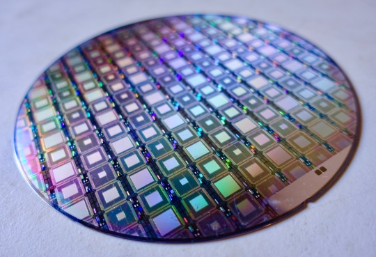
Quantum computing
#wafer#semiconductor#silicon wafer#quantum computing#quantum computer#wikipedia#wikipedia pictures#tech#technology#techcore#technologycore#computing#computer engineering#science
194 notes
·
View notes
Text
Quantum Computing with a Twist
The prediction that twisted semiconductor bilayers can host so-called non-Abelian states without a magnetic field holds promise for fault-tolerant quantum computing. [...] Scientists think that the performance of quantum computers could be improved by using hypothesized phases of matter known as non-Abelian states, which have the potential to encode information in an error-resistant way. But realizing a material that could host such states typically requires a powerful magnetic field, which would hinder device integration. Now three teams have predicted that non-Abelian states can form in certain semiconductor structures without a magnetic field [1–3]. If this prediction is confirmed experimentally, it could lead to more reliable quantum computers that can execute a wider range of tasks.
Read more.
13 notes
·
View notes
Text
The new theory is based on a combination of two properties of strange metals. First, their electrons can become quantum mechanically entangled with one another, binding their fates, and they remain entangled even when distantly separated. Second, strange metals have a nonuniform, patchwork-like arrangement of atoms.
#nanotechnology#materialsscience#advancedmaterials#semiconductor#quantum#electronics#computing#technology
69 notes
·
View notes
Text
Physics - φ


#physicsshirt #scienceloversgift #physicsapparel #coolphysicsdesign #phisymboltshirt #sciencehoodies #geekyfashion #physicslongsleeve #scienceteachergift #educationalclothing #nerdyoutfit #minimalistscienceshirt #geekhoodie #physicsloverapparel #funnyphysicsshirt #studentgiftidea #physicsenthusiaststyle #mathandscienceshirt #phihoodiedesign #collegestudentfashion
#physics student#physics class#physics memes#science#time#cosmos#cosmology#space#physics girl#physics studyblr#tee shirt#teespring#t shirt#shirts#womens fashion#style#clothes#outfit#clothing#fashion#accessories#hoddie#gildan#quantum physics#quantum mechanics#quantum computing#astrophysics#space exploration#optics#semiconductor
7 notes
·
View notes
Text
Equal1 Validates Complementary Metal Oxide Semiconductor
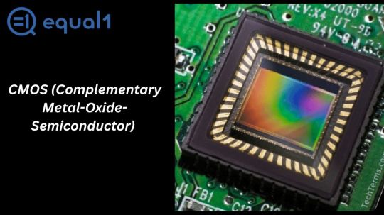
Equal1, a leader in silicon-powered quantum computing, believes the approval of a commercial CMO process represents a quantum computing milestone.
This breakthrough advances silicon-based, scalable spin qubit quantum technology in conventional semiconductor production.
Business technology advances significantly
For the first time in a commercial approach, the validation reveals that several quantum dots can have precisely regulated tunnel coupling.
Equal1 is advancing quantum computing in semiconductor frameworks by transforming multi-gate transistors into functional quantum-dot arrays, creating a benchmark for scalable spin qubit designs.
This was achieved using the GlobalFoundries (GF) 22FDX Fully Depleted Silicon-On-Insulator (FD-SOI) architecture, known for its comprehensive traditional SoC integration.
After Equal1's latest quantum computing achievement, here's a detailed description of the CMOS method:
Equal1 validated a commercial Complementary Metal Oxide Semiconductor quantum computing technique.
This is a major step towards silicon-based, scalable spin qubit quantum technologies under normal semiconductor manufacturing limits.
This proves that standard semiconductor manufacture can produce quantum systems.
Controlled production of numerous tunnel-coupled quantum dots using the GlobalFoundries 22FDX FD-SOI platform is essential to this validation.
This is a business first. Equal1 is making functional quantum-dot arrays from multi-gate transistors for scalable spin qubit systems.
This technique aims to directly integrate quantum computing into semiconductor designs.
Given its reputation for comprehensive conventional SoC integration, the GlobalFoundries 22FDX FD-SOI platform is crucial.
Equal1 uses this industry-standard silicon architecture for easy SoC integration to provide a practical and extensible quantum computing foundation.
This aligns quantum computing with Complementary Metal Oxide Semiconductor technology, which improves scalability.
Equal1 CEO Jason Lynch said the business is using CMOS-compatible technology to solve scalability and integration difficulties, enabling large-scale quantum computers.
They found that scalable quantum systems are closer than most people assume because they take use of the silicon environment.
Silicon spin qubits are intriguing prospects for scalable quantum computers due to their compatibility with Complementary Metal Oxide Semiconductor technology and intrinsic coherence.
Equal1 uses a commercial silicon platform, unlike other quantum computing devices that use exotic materials and custom fabrication methods.
Integrating quantum computing capabilities into well-established semiconductor manufacturing technologies, which power most modern devices, shows their potential for widespread usage.
Equal1's monolithic chip's 29 NMOS and PMOS quantum cells can all support linear quantum-dot arrays with up to three tunnel-coupled quantum dots and charge sensors.
These quantum dot arrays performed well and were stable at 70 mK to 1.2 K.
The promising Equal1 results demonstrate that GlobalFoundries' 22FDX quantum platform is gaining popularity, according to Ted Letavic.
He emphasises the platform's back gate, which allows quantum applications to enhance performance using an additional transistor control electrode.
GlobalFoundries wants to work with Equal1 to improve their designs and demonstrate quantum advances.
Equal1's discovery is part of a trend among silicon spin qubit firms to push semiconductor manufacturing boundaries to develop scalable quantum computing.
Quantum 2.0, a new age focussing on scalable and practical quantum systems using current technology, is beginning with these efforts.
This new age aims to produce scalable and usable quantum systems that operate with present technology infrastructures.
Conclusion
Complementary Metal Oxide Semiconductor uses standard semiconductor manufacturing methods like the GlobalFoundries 22FDX FD-SOI platform to manufacture silicon-based quantum devices like spin qubits and quantum dots. The maturity, scalability, and affordability of CMOS technology enable large-scale, realistic quantum computing devices that can be linked with conventional electronics on a chip.
#technology#technews#govindhtech#news#technologynews#Complementary Metal Oxide Semiconductor#quantum computing#Equal1#CMOS#Quantum 2.0
0 notes
Text
#quantum computing#NanoElectronics#Semiconductors#IISc#Innovation#TechLeadership#electronicsnews#technologynews
0 notes
Text
Lab-Grown Diamonds: India's Sparkling Revolution
Diamonds have long symbolized status, love, and aspiration, but behind their brilliance lies a complex narrative of environmental concerns, ethical dilemmas, and fluctuating prices. Enter lab-grown diamonds—engineered with precision, yet identical in composition to their mined counterparts. These stones are transforming the Indian market, offering consumers a sustainable, affordable, and conflict-free alternative. What once seemed a niche innovation is now disrupting traditional diamond commerce, drawing attention from millennials, investors, and even luxury brands. As India, a global diamond powerhouse, embraces this shift, the question is no longer whether lab-grown diamonds will succeed, but how quickly they will dominate. With India being one of the largest producers and consumers of diamonds, this transition holds immense significance for both the domestic and international markets.
#Lab-grown diamonds India#synthetic diamonds market#CVD diamonds#HPHT diamonds#sustainable jewelry#diamond industry trends#Indian diamond exports#affordable diamonds#ethical diamonds#luxury jewelry India#Surat diamond market#diamond technology#quantum computing diamonds#diamond-based semiconductors
0 notes
Text
Quantum Mechanics in Modern Technology: The Science Explained
Introduction
Welcome to TechtoIO! Today, we explore the intriguing world of quantum mechanics and its profound impact on modern technology. Quantum mechanics, once a purely theoretical field, is now driving innovations that are transforming industries. But what exactly is quantum mechanics, and how is it applied in today’s tech? Let’s break down the science behind this fascinating topic. Read to continue
#CategoriesScience Explained#Tagschallenges in quantum technology#entanglement in quantum mechanics#future of quantum mechanics#lasers and quantum mechanics#LEDs and quantum mechanics#modern technology#MRI and quantum mechanics#photovoltaics and quantum mechanics#quantum computing#quantum cryptography#quantum mechanics#quantum sensors#quantum teleportation#science of quantum mechanics#semiconductors and quantum mechanics#superposition in quantum mechanics#transistors and quantum mechanics#uncertainty principle#wave-particle duality#Technology#Science#business tech#Adobe cloud#Trends#Nvidia Drive#Analysis#Tech news#Science updates#Digital advancements
1 note
·
View note
Text
Compound Semiconductors: Shaping the Future of Healthcare Technology
Exploring the World of Compound Semiconductors
In the realm of modern technology, compound semiconductors stand as the backbone of innovation and progress. These advanced materials, composed of two or more elements, offer a myriad of opportunities across various industries. From telecommunications to renewable energy, compound semiconductors play a pivotal role in shaping the future.
The Power of Compound Semiconductors Unleashed
Compound semiconductors exhibit unique properties that set them apart from traditional silicon-based semiconductors. With superior electron mobility and enhanced thermal conductivity, they pave the way for faster and more efficient electronic devices. This opens doors to groundbreaking advancements in computing, telecommunications, and beyond.
Applications Across Diverse Industries
Revolutionizing Telecommunications
In the ever-evolving landscape of telecommunications, compound semiconductors are driving innovation at an unprecedented pace. Their ability to operate at higher frequencies enables the development of ultra-fast communication networks, facilitating seamless connectivity for billions worldwide.
Empowering Renewable Energy
The quest for sustainable energy solutions finds a formidable ally in compound semiconductors. From solar cells to LED lighting, these materials optimize energy conversion and storage processes, ushering in a new era of clean and efficient power generation.
Enhancing Healthcare Technologies
In the realm of healthcare, precision and reliability are paramount. Compound semiconductors play a vital role in powering medical devices, from diagnostic equipment to advanced imaging technologies. Their exceptional performance ensures accurate diagnoses and effective treatments, ultimately improving patient outcomes.
Future Prospects and Innovations
As research and development in compound semiconductor technology continue to advance, the possibilities are limitless. Emerging trends such as quantum computing and nanotechnology hold the promise of revolutionizing industries and reshaping our understanding of the world.
Supporting the Journey of Innovation
The journey towards harnessing the full potential of compound semiconductors requires support and collaboration. By fostering partnerships between academia, industry, and government agencies, we can accelerate the pace of innovation and drive meaningful change.
Conclusion: Pioneering the Next Frontier
In conclusion, compound semiconductors represent the cornerstone of modern technological advancement. With their unparalleled performance and versatility, they hold the key to unlocking a future defined by innovation, sustainability, and progress. Embracing the potential of compound semiconductors is not just a choice; it's a commitment to shaping a better tomorrow for generations to come.
#Compound Semiconductors#Technology Advancements#Telecommunications#Renewable Energy#Healthcare Technologies#Quantum Computing#Sustainable Energy Solutions#Innovation#Nanotechnology#Future Technologies
0 notes
Text
Dean Obeidallah at The Dean's Report:
“The one big thing nobody is talking about: Did Elon want to shut the government down because of his business deals with China?” That was the first line of Rep. Jim McGovern (D-Mass) multi-part statement Saturday posted on Elon Musk’s platform, X--ironically enough. A similar point was also made Friday by Rep. Rosa DeLauro (D-CT)—the ranking minority member of the House Appropriations Committee-in a detailed letter to leaders of the House and the Senate. What was the issue the two were flagging? As Rep. McGovern wrote: “The original funding bill (that he [Musk] killed) included what’s called an “outbound investment” provision—which would limit & screen U.S. money flowing to China. That would have made it easier to keep cutting-edge AI and quantum computing tech—as well as jobs—in America. But Elon had a problem.” DeLauro gave even more context to this provision vetting investments in China: “This outbound investment provision was agreed to after months of bipartisan, bicameral negotiations and years of advocacy from Members of Congress. It would have kept innovation and manufacturing in semiconductors, artificial intelligence (AI), quantum computing, and other cutting-edge technologies in the United States and prevented wealthy investors from continuing to offshore production and U.S. intellectual property into China – benefiting only their bottom lines and the Chinese Communist Party.” But Musk—per these two members of Congress—led the charge to block this proposed legislation because as McGovern accurately noted, Musk’s “second-largest market is China. He’s building huge factories there. His bottom line depends on staying in China’s good graces.” The result was that when the new budget deal was agreed upon Friday, guess what was missing? Yep, the provision that would’ve been bad for Musk’s business deals with the Chinese Communist Party—which is in essence Musk’s business partner as the NY Times detailed earlier this year in an article titled, “How Elon Musk Became ‘Kind of Pro-China.’” (Musk’s exact words.)
Rep. DeLauro explained in more detail the financial incentive behind Musk’s action to block this provision: “Musk’s car company, Tesla has poured billions of dollars into investments in China, particularly its “gigafactory” in Shanghai. The Shanghai plant is Tesla’s largest car manufacturing facility – the Chinese gigafactory produced about 50 percent of Tesla’s global automobile output over the last year.” DeLauro continued, “And in May of this year, Tesla broke ground on a new $200 million factory to manufacture large batteries critical to its electric vehicle supply chain…Notably, proponents of regulating U.S. investment in China have advocated for the inclusion of large battery manufacturing in the list of technologies subject to outbound investment screening.” Yep, these new law could’ve impacted Musk’s new business venture per DeLauro.
Rep. McGovern also raised concerns about Musk’s future business plans involving China, explaining Musk “wants to build an AI data center there too—which could endanger U.S. security.” Importantly, DeLauro detailed for all to see Musk’s documented personal relations with the Chinese Communist Party, noting, “Musk has ingratiated himself with Chinese Communist Party leadership.” For example, she cited Musk’s close ties with “Chinese premier Li Qiang, who helped rush the construction of Tesla’s Shanghai gigafactory.” DeLauro concluded her letter by writing, “It is extremely alarming that House Republican leadership, at the urging of an unelected billionaire, scrapped…this critical provision to protect American jobs and critical capabilities.” Adding, “This is particularly concerning given Elon Musk’s extensive investments in China in key sectors and his personal ties with Chinese Communist Party leadership, and calls into question the real reason for Musk’s opposition to the original funding deal.”
[...] In fact, even a well-known Republican raised alarm bells about Musk’s loyalty to Beijing. Vivek Ramaswamy--who Trump tapped with Musk to co-head the newly created Department of Government Efficiency--was publicly warning in 2023 that Musk was a puppet for the Chinese Communist Party. As CNN recently reported, Ramaswamy was concerned that “Tesla is increasingly beholden to China,” adding damningly, “I have no reason to think Elon won’t jump like a circus monkey when [China’s leader] Xi Jinping calls in the hour of need.” The GOP silence on Musk’s extensive ties to the Chinese Communist Party is beyond hypocritical given that for years Republicans have slammed China as a threat. For example, in January 2023, the House GOP created “The Select Committee on the Chinese Communist Party” designed to address the “threat posed by the Chinese Communist Party and develop a plan of action to defend the American people, our economy, and our values.” Earlier this year, the House GOP led the charge to ban Tik Tok from having access to the United States--which was signed into law and goes into effect Jan. 19, 2025 unless the Chinese company that owns the social media platform sells it to a non-Chinese company. But when it comes to Musk, the GOP doesn’t care that he has documented ties to top Chinese Communist Party officials.
CCP puppet and de facto “President” Elon Musk helped block the original CR to protect his business deals with the Chinese government, because it had an “outbound investment” provision that would screen any US money sent to China.
#Elon Musk#China#Vivek Ramaswamy#GOP Hypocrisy#Tesla#President Musk#Rosa DeLauro#Jim McGovern#CCP#US/China Relations#TikTok Ban#TikTok#DOGE#Department of Government Efficiency
13 notes
·
View notes
Text


Forgotten property of the electron
Physical discovery opens up new avenues for “orbitronics”
The orbital angular momentum of electrons has long been considered a minor physical phenomenon, suppressed in most crystals and largely overlooked. Scientists at Forschungszentrum Jülich have now discovered that in certain materials it is not only preserved but can even be actively controlled. This is due to a property of the crystal structure called chirality, which also influences many other processes in nature. The discovery has the potential to lead to a new class of electronic components capable of transmitting information with exceptional robustness and energy efficiency.
From electronics to spintronics, and now to orbitronics: In classical electronics, it is primarily the charge of the electron that counts. In modern approaches such as quantum computing and spintronics, the focus has shifted to the electron’s spin. Now, another property is entering the spotlight: orbital angular momentum (OAM). In simple terms, OAM describes how the electron moves within an atom – not in a classical orbit, but as a quantum mechanical distribution within an orbital.
“For decades, spin was considered the key parameter for new quantum-based technologies. But orbital angular momentum also has great potential as an information carrier – and is significantly more robust,” explains Dr. Christian Tusche from the Peter Grünberg Institute (PGI-6) at Forschungszentrum Jülich. The physicist is one of the lead authors of the study published in the renowned journal Advanced Materials.
The orbital angular momentum is one of the fundamental quantum numbers of the electron, similar to spin, which describes the apparent rotation of the electron. However, OAM is rarely observable in crystals. It is usually suppressed by the symmetrical electric and magnetic fields in the crystal lattice – an effect known as “quenching.”
In so-called chiral materials such as the cobalt silicide (CoSi) studied, this is different, as the team led by Christian Tusche, together with partners in Taiwan, Japan, Italy, the US, and Germany, has now been able to show. The word “chiral” comes from the ancient Greek “cheir” for hand. “These crystal structures lack mirror symmetry and are either left- or right-handed – just like the human hand. You can turn them around and they remain mirror images of each other,” explains Dr. Tusche. Chirality occurs frequently in nature. Sugar molecules, amino acids, and DNA all exhibit chiral structures.
Using high-resolution momentum microscopy and circularly polarized light, the researchers were able to resolve the orbital angular momentum in the chiral semiconductor for the first time – both inside the crystal and on its surface. For the measurements, they used the NanoESCA momentum microscope operated by Forschungszentrum Jülich at the Elettra synchrotron in Trieste, Italy. They discovered that the handedness of the crystal – left- or right-handed – predictably affects the orbital angular momentum of the electrons.
New link between crystal structure and electron
“Our results show that the structure of the crystal directly influences the angular momentum of the electrons – an effect that we were able to measure directly. This opens up a whole new door for materials research and information processing,” emphasizes Jülich experimental physicist Dr. Ying-Jiun Chen.
Dr. Dongwook Go, theoretical physicist at the Peter Grünberg Institute (PGI-1) in Jülich, adds: “The discovery is particularly important for the emerging field of orbitronics, which uses orbital angular momentum as an information carrier for the next generation of quantum technology.”
A characteristic feature of the resulting orbital angular momentum texture are differently formed Fermi arcs: open, arc-shaped structures that become visible in so-called momentum space representations, as generated by momentum microscopy. This opens up new perspectives for applications: In the future, information could be transmitted and stored not just via the charge or spin of electrons, but also through the direction and orientation of their orbital angular momentum. This so-called orbitronics – electronics based on orbital properties – could thus provide the foundation for a new class of electronic devices.
Potential for different applications
The EU is funding the development of this future technology as part of the EIC Pathfinder project OBELIX, in which Prof. Yuriy Mokrousov from the University of Mainz is also involved. The theoretical physicist is also group leader at the Peter Grünberg Institute (PGI-1) in Jülich and contributed fundamental theoretical models to the recent discovery.
Prof. Claus Michael Schneider also sees great promise: “For instance, it seems conceivable to use orbital angular momentum as an information carrier. Or one might employ circularly polarized light to selectively influence a crystal’s chirality, enabling a light-controlled, non-mechanical switch as an alternative to the transistor. Furthermore, coupling between orbital angular momentum and spin could allow integration into existing spintronics concepts—for example, in hybrid quantum devices,” says the director of the Peter Grünberg Institute for Electronic Properties (PGI-6) at Forschungszentrum Jülich.
TOP IMAGE: View into the NanoESCA momentum microscope Credit Forschungszentrum Jülich
CENTRE IMAGE: Textures of the orbital angular momentum with mirror-image Fermi arcs that depend on the handedness of the crystal. Credit K. Hagiwara, Y.-J. Chen, D. Go, Advanced Materials 2025, https://doi.org/10.1002/adma.202418040, CC BY 4.0
LOWER IMAGE: Top: The orbital angular momentum describes the movement of the electron around the atomic nucleus. Bottom: Atomic orbitals describe the probability of finding the electrons in a particular location. Credit Forschungszentrum Jülich
3 notes
·
View notes
Text
Mesoporous silicon: Etching technique reveals unique electronic transport properties
Silicon is the best-known semiconductor material. However, controlled nanostructuring drastically alters the material's properties. Using a specially developed etching apparatus, a team at HZB has now produced mesoporous silicon layers with countless tiny pores and investigated their electrical and thermal conductivity. For the first time, the researchers elucidated the electronic transport mechanism in this mesoporous silicon. The material has great potential for applications and could also be used to thermally insulate qubits for quantum computers. The work is published in Small Structures. Mesoporous silicon is crystalline silicon with disordered nanometer-sized pores. The material has a huge internal surface area and is also biocompatible. This opens up a wide range of potential applications, from biosensors to battery anodes and capacitors. In addition, the material's exceptionally low thermal conductivity suggests applications as thermal insulator.
Read more.
15 notes
·
View notes
Text
Almost all types of quantum technology – based on the strange behaviour of particles at the subatomic level – involve spin. As they move, electrons usually form stable pairs, with one electron spin up and one spin down. However, it is possible to make molecules with unpaired electrons, called radicals. Most radicals are very reactive, but with careful design of the molecule, they can be made chemically stable.
#nanotechnology#materialsscience#advancedmaterials#semiconductor#quantum#electronics#computing#technology
32 notes
·
View notes
Text
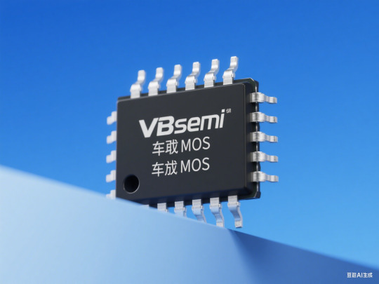
🔥 2025 MOS Electronics Deep Dive: The Tipping Point of Tech Disruption & Industry Reshaping 🔥

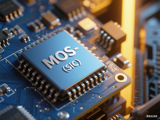
💥 Price Revolution! SiC MOSFETs Ignite Domestic Replacement Era 💥 Chinese IDM makers achieve historic breakthroughs: SiC MOSFET unit prices now undercut silicon-based IGBTs and super-junction MOSFETs at equivalent power ratings – a landmark "price inversion". Companies like BASiC Semiconductor slash module costs to 70% of imported solutions via 8-inch wafer mass production and vertical integration, boosting system efficiency by 15%. VBsemi amplifies this advantage with proprietary substrate-thinning and wafer-level testing, achieving 92% wafer utilization and 18% YoY cost reduction. Their SiC modules demonstrate 12% lower switching loss than global rivals in BYD’s 800V platform tests, fueling China’s transition from tech follower to cost leader. Projected 2025 SiC adoption: >30% in EVs, with rapid expansion in solar inverters and charging piles.
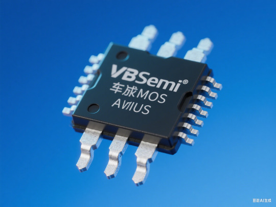
🚗 Automotive-Grade MOS Survival Thresholds: From AEC-Q101 to 800V Platforms 🚗 EV intelligence demands high-voltage/high-frequency solutions. Infineon’s OptiMOS™ 7 cuts RDS(on) by 25% and boosts switching speed by 20% using copper-clip packaging and 12-inch thin-wafer tech. BYD’s 2025 sourcing prioritizes diodes/transistors for power modules, while SemiDrive’s ASIL-D certified MCUs and GigaDevice’s GD32A503 secure major shares. VBsemi’s automotive MOS family, AEC-Q101 Grade 0 certified, features a tri-clad copper bonding structure reducing thermal resistance by 40%. Validated in XPENG’s brake-by-wire systems, it delivers millisecond response at -40°C with <10 PPM failure rates – setting new benchmarks for domestic reliability.
🌐 AI Compute Arms Race: DrMOS & Advanced Packaging Dual Fronts 🌐 NVIDIA’s GB300 NVL72 systems will drive 2025 DrMOS demand beyond 150M units, with AOS (70% share) as key supplier. NVIDIA’s cost-optimized 5x5mm DrMOS increases per-rack usage by 30% while halving unit prices, lifting server efficiency by 35%. TSMC’s CoWoS expansion and Chinese OSATs’ FOPLP/Chiplet projects push inter-chip bandwidth past 900GB/s. VBsemi’s next-gen DrMOS with Intelligent Phase Extension delivers 180A phase current in 5x5mm packages, accelerating dynamic response by 50%. Currently validating with Inspur, it boosts NVIDIA H100 GPU power efficiency by 0.8%, saving >$2,800/year per rack in electricity.
🌱 Circular Economy Reshapes Supply Chains: Recycling Boom to Lead-Free Wave 🌱 E-waste recycling surges in Shenzhen/Dongguan, with ICs fetching up to $23/PCS. EU’s 2026 lead-free mandate spurs demand for eco-components. VBsemi’s GreenMOS™ platform pioneers tin-whisker-resistant alloys and lead-free pre-plating, achieving 98% recyclability. Their super-junction MOS series passes IEC 61215 salt-mist certification, reducing coastal solar farm failures by 70%. BYD/CATL’s closed-loop systems target 85% material reuse by 2025.
🔋 Material Revolution: Silicon to Quantum Tunneling Breakthroughs 🔋 Third-gen semiconductors advance in parallel: TYSiC’s 8-inch SiC wavers hit 85% yield with 1.6% resistivity uniformity; Origin Quantum’s 72-qubit "Wukong" chip and IBM’s 1000-qubit processor mark quantum leaps. VBsemi’s hybrid gate-oxide tech (co-developed with CAS) slashes GaN HEMT gate leakage by 1,000x, enabling 97.2% efficiency at 2400V. Deployed in Huawei’s chargers, it achieves record 6.8W/cm³ power density.
💡 The Next Decade: From "China Replacement" to "Global Redefinition" 💡 Per BCG, 2025 global semiconductor market rebounds to $650B (AI chips +35%, consumer electronics +3%). China reconfigures supply chains via "wafer-fab origin" rules: SMIC’s 28nm capacity grows 5x in 3 years with 52% domestic equipment; JCET’s advanced packaging runs at >85% utilization. As Cambricon’s computing-in-memory chips rival global leaders and YMTC’s 128L NAND forces Samsung to cut prices by 15%, a multipolar tech era accelerates – with VBsemi’s innovations at its core.
👉 Follow #MOSElectronics #ChipRevolution #TechSovereignty for industry pulse!

#mosfet#semiconductor#electronics#mosfets#popular science animation#technology#circuit#electronic#munich#youtube
2 notes
·
View notes
Text
Unlocking the Future: How Intel is Shaping Tomorrow's Technology Landscape
Introduction
In a world that is increasingly defined by technological advancements, few companies have had as profound an impact as Intel. Founded in 1968, Intel Corporation has been at the forefront of semiconductor innovation, shaping not just computing but various facets of modern life. From personal computers to cloud computing and artificial intelligence, Intel’s influence permeates every layer of technology today. The question is—how does Intel continue to unlock the future? In this article, we will explore how Intel is shaping tomorrow's technology landscape through innovation, research, sustainability efforts, and strategic partnerships.
Unlocking the Future: How Intel is Shaping Tomorrow's Technology Landscape
At its core, unlocking the future involves leveraging cutting-edge technologies to solve current challenges while also anticipating future demands. For Intel, this means investing heavily in research and development (R&D) to remain competitive in the rapidly evolving tech arena. With products that range from microprocessors to advanced AI systems, Intel stands as a pillar of innovation.
The Evolution of Semiconductor Technology A Brief History of Semiconductor Development
To truly grasp how Intel shapes technology today, it's important to understand the evolution of semiconductors. Initially developed in the 1950s and '60s, semiconductors revolutionized electronics by allowing devices to become smaller and more efficient. Intel’s introduction of the first microprocessor Get more information in 1971 marked a significant turning point in computing history.
Current Trends in Semiconductor Technology
Today, semiconductor technology continues to evolve at an astonishing pace. Innovations such as 3D chip designs and quantum computing are on the horizon. Companies like Intel are not just keeping up—they are leading these trends through relentless R&D.
Intel's Role in Artificial Intelligence Pioneering AI Technologies
Artificial intelligence represents one of the most promising frontiers for technological advancement today. Intel has made significant strides in developing AI technologies that enhance machine learning capabilities across various sectors—from healthcare to finance.
Real-World Applications of AI Solutions
AI solutions offered by Intel can be seen in applications ranging from predictive analytics in healthcare to autonomous vehicles. These advancements not only improve efficiency but also pave the way for new business models.
Cloud Computing: The New Frontier Intel's Cloud Strategy
As businesses migrate to cloud-based solutions, Intel plays a crucial role by providing powerful processors designed specifically for cloud environments. Their Xeon processors enable data centers to run efficiently and scale dramatically.
youtube
Benefits for Businesses Adopting Cloud Solutions
Companies adopting cloud solutions with Intel technologies benefit from improved security features and reduced operational costs. This shift allows businesses to focus on innovation rather than infrastructure management.
Sustainability Initiatives at Intel Commitment to Green Technology
2 notes
·
View notes