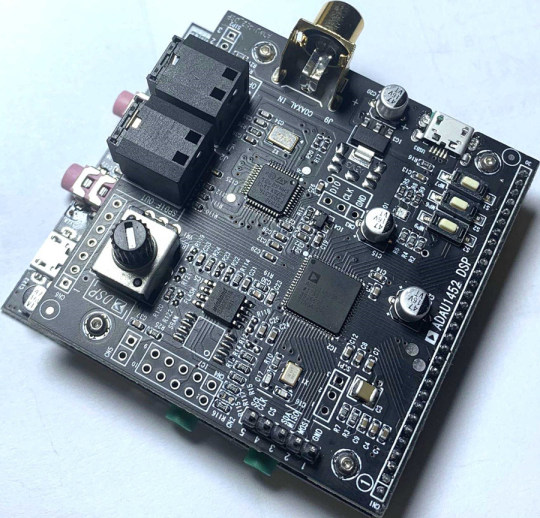
#Reflow Soldering Machine
Explore tagged Tumblr posts
Visit Tumblr Blog
Explore Tumblr blogs with no restrictions, modern design and the best experience.
Last Seen Tumblr Blogs


Fun Fact
The Tumblr office adopted Tommy, an 11-year-old Pomeranian.
Text

Enhance your production floor with a durable and ergonomic Industrial Workstation from Yontro Mechatronic Systech. Designed for efficiency, safety, and comfort, our workstations are ideal for electronics assembly, inspection, and testing processes. With customizable layouts, sturdy construction, and integrated ESD protection, Yontro’s industrial workstations help streamline operations and improve worker productivity. Trusted by manufacturers across India, we deliver quality solutions built to last.
#reflow soldering machine#yontro mechatronic systech#conveyor belt manufacturers in india#flat belt conveyor#conveyor belt#wave soldering machine#industrial work station#cleated belt conveyor
0 notes
Text
i know it' not this reductively simple, but i'm trying to sorta hone in on why i feel so untrusting of modern technology....
an analogue clock can be made by a clockmaker, by a person, with metals and tools. the metals have to come from somewhere and the tools need to be made, but that can be done by other people.
a digital clock has to be made by corporations. it needs ICs and PCBs, transistors and semiconductors, layers of phosphors and rare earth metals deposited in layers so thin your eyes can't see them, assembled together and reflow soldered by machines that are themselves too complex to be built by a person, down and down for layers. sure if you wanna pedantically miss the point i could buy the parts and solder them together myself, i can program a microcontroller, but none of that tech gets into my hands without being made by strata of corporations, and all harm they cause by squeezing enough blood from the proverbial stone in order to do it at shareholder-pleasing profit.
analogue clocks are made by people, digital clocks are made by corporations... and while supply chains cling to the crumbling cliff of the modern global world, the kids don't know how to read the analogue clock we have sitting on the bench.
16 notes
·
View notes
Text
What is PCB Assembly ?
PCB Assembly manufacturer - Hitech Circuits Co., Limited
It’s the step in the manufacturing process in which you populate a blank board with the electronic components needed to make it into a functional printed circuit board. It’s these components that make a board into the circuit that enables an electronic product to function. PCB assembly typically takes place via one of two processes:
1. Surface-mount technology
SMT: SMT stands for “Surface Mount Technology“. The SMT components are very small sizes and comes in various packages like 0201, 0402, 0603, 1608 packages for resistors and capacitors. Similarly for Integrated circuits ICs we have SOIC, TSSOP, QFP and BGA.
The SMT components assembly is very difficult for human hands and can be time taking process so it is mostly done by automated pick and place machine.
2. Through-hole manufacturing
THT: THT stands for “Through hole Technology”. The components with leads and wires, like resistors, capacitors, inductors, PDIP ICs, transformers, transistors, IGBTs, MOSFETS are example.
The component has to be inserted on one side of PCB and pulled by leg on other side and cut the leg and solder it. The THT components assembly is usually done by hand soldering and is relatively easy.
Printed Circuit Board Assembly Techniques
There are only two common PCBA techniques available for use by a PCB designer. The methods are:
1. Automated PCB Assembly Techniques
Generally, this technique employs the use of state of the art machines, which are fully automatic. For example, the surface mount components are worth positioning with the aid of an automated pick and place machine.
Again, reflow soldering is commonly for surface mount components usually done in a reflow oven. An automated solder stencil is also used to apply the solder paste on the PCB.
Finally, high tech inspection machines are used to confirm and check the quality of the PCBA. Some of which include: Automated optical inspection machine (AOI), X-ray inspection machines, etc.
Above all, due to the precise monitoring, control of soldering, no human input and versatile machines.
This technique ensures utmost efficiency, output consistencies, and limits defects.
2. Manual PCB Assembly Techniques
This method is favorite for use with through-hole parts, which needs manual placement on the board. Besides, with these through-hole parts, it’s advisable you use wave soldering. Note that in the through- hole assembly process, you need to place the components and electronics on the PCB.
After that, you use wave soldering to solder the leads. Typically, you will need an individual to insert a component into a marked PTH. Once done, transfer the PCB to the next station where the next person will be on standby tasked with fixing another part.
What are the Benefits of SMT PCB Assembly?
SMT assembly provides many benefits and some of them are as follows:
It can be used to incorporate small components.
In SMT, the components can be placed on both sides of the board.
It assures high component densities.
Fewer holes need to be drilled for surface mounting than through-hole.
It require low initial costs and time for setting up the mass production.
SMT is the simpler and faster-automated assembly when compared to through-hole.
Errors regarding the component placement can be easily rectified.
Surface mount PCBs feature strong joints, which can easily withstand vibrations.
What are the techniques used in Surface Mount Technology?
There are several techniques for the reflow process. After applying the solder paste or a flux mixture on the board and after placing the components, the boards are conveyed to a reflow soldering oven. The techniques used for reflowing soldering include infrared lamps, hot gas convection, fluorocarbon liquids with a high boiling point, and so on.
What are the different testing methods used in SMT PCB Assembly?
Hitech Circuits as the PCB assembly manufacturer, we perform the following testing and inspection to ensure the quality of surface mount PCBs.
Automated Optical Inspection (AOI): This is performed before and after the soldering to identify the component placement, presence, and solder quality.
X-ray Testing: In this type of testing, the operator relies on the X-ray images of the PCB to check the solder joints and lead-less components such as Quad Flat Packs and ball grid arrays, which are generally not visible to naked eyes.
In-Circuit Testing (ICT): This method is used to detect manufacturing defects by testing the electrical properties in the SMT Assembly.
What type of files or documents should I send for SMT PCB Assembly?
Gerber Files: The file contains all details of physical board layers including solder masks, copper layers, drill data, legends, and so on.
Bill of Materials (BOM): This contains information on the list of items needed for the PCB manufacturing and the instructions of manufacturing.
Pick and Place File: This file contains information on all components to be used in the PCB design and their rotation and X-Y coordinates.
The whole process of PCB Assembly
1. Bare board loader machine
The first step in the PCB assembly is to arrange the bare boards on the rack, and the machine will automatically send the boards one by one into the SMT assembly line.
2. Printing solder paste
When PCB on the SMT production line, firstly, we have to print solder paste on it, and the solder paste will be printed on the pads of the PCB. These solder pastes will be melt and solder the electronic parts to the circuit board when it passes through the high-temperature reflow oven.
In addition, when testing new products, some people will use film board/adhesive cardboard instead of solder paste, which can increase the efficiency for adjusting the SMT machines.
3. Solder paste inspection machine(SPI)
Since the quality of solder paste printing is related to the quality of welding of subsequent parts, some SMT factories will use optical machine to check the quality of solder paste after printed the solder paste in order to ensure stable quality. If there any poorly printed solder paste board, we will wash off the solder paste on it and reprint, or remove the excess solder paste if there is redundant solder paste on it.
4. High speed SMT machine
Usually, we will put some small electronic parts (such as small resistors, capacitors, and inductors) to be printed on the circuit board first, and these parts will be slightly stuck by the solder paste just printed on the circuit board, so even if the speed of printing is very fast and the parts on the board will not fall away. But large parts are not suitable for use in such high speed SMT machines, which will slow down the speed of small parts assembly. And the parts will be shifted from the original position due to the rapid movement of the board.
5. Universal SMT machine
Universal SMT machine is also known as "slow machine", it will be assembled some large electronic components, such as BGA IC, connectors, etc., these parts need more accurate positions, so the alignment is very important. Use a camera to take a picture to confirm the position of the parts, so the speed is much slower than High speed SMT machine we taked before. Due to the size of the components here, not all of them are packed in tape and reel, and some may be packed in trays or tubes. But if you want the SMT machine to recognize the trays or tube-shaped packaging materials, you must configure an additional machine.
Generally, traditional SMT machines are using the principle of suction to move electronic parts, and in order to place the parts successfully, and there must be the flat surface on these electronic components for the suction nozzle of the SMT machine to absorb. However, for some electronic parts don’t have a flat surface for these machines, and it is necessary to order special nozzles for these special-shaped parts, or add a flat tape on the parts, or wear a flat cap for thees electronic parts.
6. Manual parts or visual inspection
After assembled all parts by the high speed SMT machine or Universal SMT machine and before going through the high-temperature reflow oven, and we will set up a visual inspection station here and to pick out the deviation parts or missing components boards etc., because we have to use a soldering iron to repair if there are still defectives boards after passing the high-temperature oven, which will affect the quality of the product and will also increase the cost. in addition, for some larger electronic parts or traditional DIP parts or some special reasons cannot be processed by the SMT machine before, they will be manually placed on pcb here.
7. Reflow oven
The purpose of reflow oven is to melt the solder paste and form a non-metallic compound on the component feet and the circuit board, that means to solder electronic components on the circuit board. The temperature rise and fall curves often affect the soldering quality of the entire circuit board. According to the characteristics of the solder materials, usually the reflow oven will set the preheating zone, soaking zone, reflow zone, and cooling zone to achieve the best soldering effect.
For example, the melting point for SAC305 solder paste with lead-free is about 217°C, which means that the temperature of the reflow oven must be higher than the melting points to remelt the solder paste. What's more, the maximum temperature in the reflow furnace should not exceed 250°C, otherwise many parts will be deformed or melted because they cannot withstand such a high temperature.
Basically, after the pcb passed through the reflow oven, the assembly for the entire circuit board is almost complete. If there are hand-soldered parts, we need to transfer to DIP process, and then we have to check the quality after reflow oven by QC department.
8. Automatic optical inspection(AOI)
The main purpose of setting up AOI is because some high density boards can’t be process the following ICT test, so we used AOI inspection to replace it. But even using AOI inspections, there still have the blind spots for such checking, for example, the solder pads under the components cannot be checked by AOI. At present, it can only check whether the parts have side standing issue, missing parts, displacement, polarity direction, solder bridges, lack of soldering etc., but cannot checking the BGA solderability, resistance value, capacitance value, inductance value and other components quality, so far AOI inspection can’t completely replace ICT test.
Therefore, there is still some risk if only AOI inspection is used to replace ICT testing, but ICT test is also not 100% make sure the good quality, we suggest these two ways can be combined with together to make sure the good quality.
9. PCB unloader machine
After the board is fully assembled, it will be retracted to the unloder machine, which has been designed to allow the SMT machine to automatically pick and place the board without damaging the quality for PCB.
10. Visual inspection for finished products
Normally there will be a visual inspection area in our SMT production line whether there is an AOI station or not, and it will help to check if there are any defectives after completed assembled the pcbs. If there is an AOI station, it can reduce the visual inspection worker on our SMT line, and to reduce the potential cost, and because it is still necessary to check some places that cannot be judged by AOI, many SMT factories will provide the mainly visual inspection templates at this station, which is convenient for visual inspection worker to inspect some key parts and polarity for components.
11. DIP process
DIP process is a very important process in the whole PCBA processing, and the processing quality will directly affect the functional for PCBA boards, so it is necessary to pay more attention to the DIP process. There are many preliminary preparations for DIP process. The basic process is to re-process the electronic components first, like to cut the extra pins for some DIP components, our staff received the components according to the BOM list, and will check whether the material part numbers and specifications are correct or not, and performs pre-production pre-processing according to the PCBA samples. The steps are: Use various related equipment (automatic capacitor pins cutting machine, jumper bending machine, diode and triode automatic forming machine, automatic belt forming machine and other machines) for processing.

12. ICT test
Printed Circuit board open/short circuit test (ICT, In-Circuit Test), The purpose of ICT test is mainly to test whether the components and circuits on the printed circuit board are open or short issues. It can also measure the basic characteristics of most components, such as resistance, capacitance, and inductance values to judge whether the functions of these parts are damaged, wrong parts or missing parts etc. after passing through the high-temperature reflow oven.
ICT test machines are divided into advanced and basic machines. The basic ICT test machines are generally called MDA (Manufacturing Defect Analyzer). It’s just to measure the basic characteristics of electronic components and judge open and short circuits issue we talked above.
In addition to all the functions of the basic ICT test machines, for advanced ICT test machine can also test the whole PCBA by using power, start to testing the PCBA boards by setting the program in the test machine. The advantage is that it can simulate the function of the printed circuit board under the actual power-on condition, this test can partly replace the following functional test machine (Function Test). But the cost for the test fixture of this advanced ICT test can probably buy a car, it’s too expensive and we suggest it can be used in mass production products.
13. PCBA function test
Functional testing is to make up for the ICT test, because ICT only tests the open and short circuits on the the PCBA board, and other functions such as BGA and other fuctions are not tested, so it is necessary to use a functional testing machine to test all functions on the whole PCBA board.
14. Cutting board (assembly board de-panel)
Normally, printed circuit boards will be produced in panel, and it will be assembled to increase the efficiency of SMT production. It means several single boards in one panel, such as two-in-one, four-in-one etc. After finished all the pcb assembly process, it needs to be cut into single boards, and for some printed circuit boards with only single boards also need to cut off some redundant board edges.
There are several ways to cut the printed circuit board. You can design the V-cut using the blade cutting machine (Scoring) or directly manually break off the board (not recommended). For more high density circuit boards, it will be used the professional splitting machine or the router to split the board without any damage the electronic components and printed circuit boards, but the cost and working hours will be a little longer.
Why Choose Hitech Circuits PCB Assembly Manufacturer for Your PCB Assembly Projects?
There are several PCB manufacturers specializing in PCB assemblyservices. However, Hitech Circuits PCB Assembly stands out owing to the following:
Assistance in Material Procurement:
Technically, in PCB assembly services, the quality of parts is the responsibility of the OEM; however, we ease your job by assisting you to make the right selection. We can help you procure all your parts of the same type own a single part number, thanks to our supply chain and vendor network as well as experience. This saves time and cost that goes in ordering single parts as you plan.
Testing procedures:
We are very focused on quality and thus implement stringent testing procedures at each stage of the assembly and after completion.
Fast Turnaround Times:
Our well-equipped facility and the right tools enable us to complete your requirements well before time, and without compromising on the quality or functioning of the PCBs. For simple designs we revert in 24 to 48 hours.
Cost Effectiveness:
While PCB assembly is a cost-effective alternative, we go a step further and assure that the parts you list are of a good quality and suitable for your requirement. Also, you can control the part flow and replenish them as needed. This eliminates the need to buy extra stock and store it.
Quick Quote:
We offer a quick quote based on your BOM. All you need is a detailed BOM, Gerber files, your application requirement sheet, and quantity.
We’re not one to stand still, which is why we use the latest equipment and the finest minds to create your PCB projects. We’re constantly keeping our finger on the pulse of the latest trends. And as a result, we know how to deliver the highest standards of PCB assembly to meet all your requirements.
Our dedicated, friendly customer service team also means that we support you every step of the way. Offering our expert guidance to ensure a complete PCB project that you’re happy with.
Contact us today
No matter what your printed circuit board assemblyneeds are, we always aim to deliver efficient, dependable solutions. For more information about our services, do not hesitate to get in touch with us today for a no-obligation quote
2 notes
·
View notes
Text
Soldering Innovations: What’s Next for Industrial Applications?
In the fast-evolving Hiflo solders world of electronics and industrial manufacturing, soldering technology is no longer just a routine process; it’s becoming a strategic differentiator. From consumer gadgets to electric vehicles and aerospace systems, soldering plays a critical role in assembling complex electronic circuits and ensuring long-term reliability.
With industries demanding higher efficiency, sustainability, and miniaturization, the future of soldering is shifting toward smarter, safer, and more adaptable innovations. So, what’s next for industrial applications? Let’s explore the soldering trends that are reshaping the way modern industries function.
🔬 1. Rise of Lead-Free and RoHS-Compliant Alloys
One of the most significant transformations in recent years is the move toward lead-free solder. Driven by environmental and health regulations like RoHS (Restriction of Hazardous Substances), industries are moving away from traditional lead-based soldering alloys.
Alloys like SAC305 (Sn96.5/Ag3.0/Cu0.5) are now widely adopted across automotive, aerospace, and consumer electronics sectors. These alloys not only meet compliance standards but also offer strong mechanical and thermal performance.
At HiFlo Solders Pvt. Ltd., we manufacture RoHS-compliant solder wires and bars that ensure safety without compromising quality, making them ideal for both mass production and sensitive electronic applications.
🤖 2. Automation and Smart Soldering Machines
Industrial soldering is becoming smarter with automated soldering systems and AI-powered robotics entering the scene. These machines ensure precise control of temperature, pressure, and timing — reducing human error and improving repeatability.
Smart soldering irons equipped with IoT technology can collect data in real-time, helping manufacturers track performance, detect anomalies, and maintain consistency.
In high-volume sectors like automotive PCB assembly or LED lighting, automated wave soldering and reflow soldering machines are now the norm. The future is all about connected, intelligent, and data-driven soldering systems.
🔍 3. Nano Soldering and Miniaturization
As electronic devices become smaller and more compact, the soldering processes used in manufacturing must evolve. Enter nano soldering — a precision technique used for ultra-fine solder joints on microchips and tiny components like sensors, MEMS, and medical devices.
Micro-soldering stations are increasingly used in R&D labs and mobile repair centers. This innovation is critical for industries like wearables, IoT, and biomedical devices, where component size is measured in microns.
In future applications, laser-assisted soldering and ultrasonic soldering may take over traditional hand methods, especially where heat sensitivity is a concern.
🌱 4. Eco-Friendly Soldering Flux and Chemicals
Sustainability is a key driver in modern manufacturing. Traditional soldering processes use fluxes and pre-cleaning chemicals that may be harmful to workers and the environment. Today, companies are investing in eco-friendly flux formulations, low-residue, and VOC-free chemicals to reduce their carbon footprint.
At HiFlo Solders, we are constantly researching environmentally safe pre-soldering chemicals and low-emission solder pastes that ensure worker safety and environmental compliance.
📦 5. Advanced Solder Materials: Beyond Tin and Lead
The future also lies in advanced solder alloys designed for high-performance and extreme environments. For example:
Bismuth-based solders: For low-temperature applications.
Silver-rich alloys: For aerospace and defense where strength and conductivity are critical.
Indium alloys: For cryogenic applications and soft soldering in semiconductors.
These innovations offer tailored solutions to meet the needs of various industries and unique operating conditions.
🔄 6. Sustainability Through Recyclable and Reusable Solder
Another growing trend is the development of recyclable solder materials. Manufacturers are exploring solder formulations that can be recovered, purified, and reused multiple times — reducing both waste and production cost.
This aligns with global sustainability goals and circular economy principles. HiFlo Solders is also investing in recycling initiatives for solder dross and scrap material, contributing to an eco-friendly industrial ecosystem.
📈 Final Thoughts: The Future is Smart, Green & Precise
The next era of industrial soldering is focused on three pillars:
Smart automation
Green chemistry
Precision materials
As industries become more digital, interconnected, and environmentally aware, soldering innovations must keep pace. Companies like HiFlo Solders Pvt. Ltd. are leading the charge by combining research-driven manufacturing, quality-focused production, and customer-specific customization.
Whether you’re in the business of manufacturing PCBs, medical devices, EVs, or industrial electronics, staying updated with next-gen soldering technologies is essential for long-term success.
🔗 Looking for reliable, RoHS-compliant solder wires or custom solder bars?
Website : 👉 Explore our range at www.hiflosolders.com
0 notes
Text
What Are the Advantages of SMT Processing Technology Compared to DIP?
In today's mass-produced electronic hardware, a significant portion utilizes Surface Mount Technology (SMT) processing, which has become an industry trend.
Surface Mount Technology for High-Speed PCBA Processing
From a developmental perspective, the widely adopted SMT soldering process today is essentially a derivative and upgraded version of the DIP (Through-Hole Technology) plug-in process. When using SMT, only the quality of PCB pads needs to be considered, eliminating the need for drilling. This not only significantly improves production speed but also greatly simplifies the process. Although SMT may not offer the same seismic stability as through-hole mounting in certain special environments, its advantages still make it suitable for large-scale application.
Five Key Stages of the SMT Process
PCB Production: This stage focuses on manufacturing the PCB, with emphasis on the quality of solder pads.
Solder Paste Printing: Applying solder paste onto the pads to prepare for the next mounting step.
Component Placement: A pick-and-place machine precisely positions components on the solder paste-printed pads through programming.
Reflow Soldering: Bonding components firmly to the pads via reflow soldering.
PCBA Finishing/Testing/Shipping: Assembling, testing, and delivering the finished PCBA.
Differences Between SMT and DIP Through-Hole Technology
Space Optimization: Through-hole mounting often suffers from space constraints, which SMT addresses effectively. SMT components are smaller and more flexibly arranged, allowing a higher component density per unit area. This enables more powerful functionality in smaller spaces, whereas through-hole mounting has the opposite effect.
Faster Circuit Speed: Reduced component size contributes to higher circuit operation speeds.
Superior Vibration Resistance: SMT has proven more stable in high-vibration or shaking environments.
Cost Efficiency: SMT components typically cost less than their through-hole counterparts.
Shorter Production Cycle: The elimination of drilling significantly shortens SMT production time, accelerating manufacturing and reducing time-to-market. This makes SMT an ideal choice for new product development. Using Design for Manufacturability (DFM) software tools further minimizes rework and redesign needs for complex circuits, enhancing the speed and feasibility of intricate designs. [View the guide on why process control measurements are crucial for preventing defects in SMT PCB assembly.](Link to relevant resource)
If you’re interested in PCB&PCBA products, pls kindly email to Sandy: [email protected]
1 note
·
View note
Text
What Is Reflow Soldering in Surface-Mount Technology?
Surface-mount technology (SMT) is a cornerstone of modern electronics manufacturing, enabling the precise assembly of electronic components onto printed circuit boards (PCBs) through processes like reflow soldering. Reflow soldering, a key technique in surface-mount technology, uses a controlled heating process within a reflow furnace to melt solder paste, forming robust electrical and mechanical connections between components and PCBs. This method is critical in surface-mount technology for its efficiency and ability to handle complex, high-density assemblies. This article, inspired by innovations from companies like Chengliankaida Technology Co., Ltd., explores the reflow soldering process in surface-mount technology, its stages, benefits, challenges, and its pivotal applications in electronics manufacturing.
How Does the Reflow Soldering Process Work in Surface-Mount Technology?
In surface-mount technology, reflow soldering is a meticulously orchestrated process comprising several stages, each designed to ensure reliable solder joints for components mounted on PCBs. These stages are critical to the success of surface-mount technology in producing high-quality electronic assemblies.
Solder Paste Application in Surface-Mount Technology
The reflow soldering process in surface-mount technology begins with applying solder paste—a blend of powdered solder and flux—onto PCB solder pads. This is typically done using a screen-printing process, where a stencil ensures precise deposition of solder paste in surface-mount technology applications. The paste temporarily secures components, setting the stage for reliable connections in surface-mount technology assemblies. The quality of solder paste is crucial, as it impacts the integrity of solder joints in surface-mount technology.
Component Placement in Surface-Mount Technology
Following solder paste application, automated pick-and-place machines position components onto the PCB with exceptional accuracy in surface-mount technology. These machines use advanced vision systems to ensure precise alignment, a vital aspect of surface-mount technology where misalignments can lead to defective solder joints. Accurate component placement is essential for the success of reflow soldering in surface-mount technology, ensuring robust connections.
Preheating Stage in Surface-Mount Technology
Once components are placed, the PCB enters the reflow furnace for the preheating stage in surface-mount technology. Here, the temperature gradually rises to activate the flux, which cleans surfaces by removing oxides and contaminants. This stage also eliminates moisture, reducing thermal shock risks in surface-mount technology. Controlled preheating is critical in surface-mount technology to protect sensitive components and ensure uniform heating across the PCB.
Thermal Soak Stage in Surface-Mount Technology
The thermal soak stage in surface-mount technology maintains a stable temperature to further activate the flux and ensure even heat distribution. This phase prepares the solder paste for melting, enhancing its fluidity for the reflow stage in surface-mount technology. Uniform thermal soak is essential in surface-mount technology to accommodate components of varying sizes and thermal properties, minimizing defects.
Reflow Stage in Surface-Mount Technology
The reflow stage is the core of the process in surface-mount technology, where the furnace reaches peak temperatures, typically 230°C to 250°C, based on the solder paste type (e.g., lead-free or leaded). The solder particles melt, forming a liquid phase that wets component leads and PCB pads, creating strong metallurgical bonds in surface-mount technology. Precise control of temperature and duration is critical in surface-mount technology to prevent overheating, which could damage components or compromise solder joint quality.
Cooling Stage in Surface-Mount Technology
After reflow, the PCB enters the cooling zone in surface-mount technology, where the temperature gradually decreases to solidify the molten solder into durable joints. Controlled cooling is vital in surface-mount technology to avoid thermal stress, which can cause defects like solder joint cracking or component warpage. A gradual cooling rate ensures reliable, high-quality connections in surface-mount technology assemblies.
What Are the Benefits of Reflow Soldering in Surface-Mount Technology?
Reflow soldering offers numerous advantages in surface-mount technology, making it the preferred method for assembling modern electronic devices.
Precision and Consistency in Surface-Mount Technology
Reflow soldering furnaces provide precise control over temperature profiles in surface-mount technology, ensuring consistent and repeatable results. This precision is crucial in surface-mount technology for achieving high-quality solder joints, reducing defects, and enhancing device reliability. Advanced furnaces employ real-time monitoring to optimize conditions in surface-mount technology applications.
High Throughput in Surface-Mount Technology
The automated nature of reflow soldering in surface-mount technology enables high-volume production, ideal for large-scale electronics manufacturing. Multiple PCBs can be processed simultaneously, boosting efficiency in surface-mount technology workflows. This scalability is a key advantage in surface-mount technology for meeting industry demands.
Versatility in Surface-Mount Technology
Reflow soldering in surface-mount technology is compatible with diverse component types, including fine-pitch components, ball grid arrays (BGAs), and chip-scale packages (CSPs). This versatility makes surface-mount technology ideal for complex, high-density PCB designs, accommodating the needs of modern electronics.
Minimized Thermal Stress in Surface-Mount Technology
The gradual heating and cooling stages in reflow soldering reduce thermal stress on components in surface-mount technology, lowering the risk of damage and improving reliability. This is particularly important in surface-mount technology, where components are often sensitive to temperature fluctuations.
What Challenges Arise in Reflow Soldering for Surface-Mount Technology?
Despite its benefits, reflow soldering in surface-mount technology presents challenges that require careful management.
Optimizing Temperature Profiles in Surface-Mount Technology
Achieving the ideal temperature profile in surface-mount technology is critical for successful reflow soldering. Variations in PCB design, component density, and solder paste formulation can affect thermal dynamics, necessitating precise adjustments in surface-mount technology processes.
Thermal profiling tools are often used to optimize outcomes.
Solder Paste Management in Surface-Mount Technology
The quality and handling of solder paste significantly impact reflow soldering in surface-mount technology. Factors like paste composition, viscosity, and storage conditions must be carefully managed to ensure consistent performance in surface-mount technology. Improper handling can lead to issues like solder balling or poor wetting.
Component Compatibility in Surface-Mount Technology
Certain components in surface-mount technology may have specific temperature sensitivities or require special handling during reflow. Ensuring compatibility and protecting these components in surface-mount technology applications can be challenging, often requiring customized furnace settings.
Where Is Reflow Soldering Used in Surface-Mount Technology Applications?
Reflow soldering in surface-mount technology is widely applied across industries, enabling the assembly of complex, reliable electronic devices.
Consumer Electronics
Smartphones, tablets, and laptops rely on reflow soldering in surface-mount technology to assemble numerous small, intricate components. Surface-mount technology ensures reliable connections for compact, high-performance devices.
Automotive Electronics
Automotive systems, such as engine control units and sensors, use reflow soldering in surface-mount technology to create durable solder joints capable of withstanding harsh conditions. Surface-mount technology supports the reliability required in automotive applications.
Industrial and Medical Devices
Industrial control systems and medical equipment leverage reflow soldering in surface-mount technology for dense, high-reliability PCBs. Surface-mount technology delivers the precision needed for critical applications.
Telecommunications
Networking equipment and communication devices utilize reflow soldering in surface-mount technology to achieve high-density assemblies with excellent signal integrity, meeting the demands of modern telecommunications.
Conclusion: Why Is Reflow Soldering Vital in Surface-Mount Technology?
Reflow soldering is a fundamental process in surface-mount technology, enabling the efficient and reliable assembly of electronic devices. By leveraging precise temperature control and automation, reflow soldering in surface-mount technology ensures high-quality solder joints, minimizes defects, and enhances production efficiency. Understanding its stages, benefits, and challenges is essential for optimizing surface-mount technology processes. As electronics continue to evolve, reflow soldering in surface-mount technology will remain a driving force in innovation and excellence.
#asexual#easter#artists on tumblr#margot robbie#across the spiderverse#michael cera#barbie#donald trump#rwby#ryan gosling
1 note
·
View note
Text
Surface Mounting Technology (SMT): Revolutionizing Modern Electronics Assembly
Surface Mounting Technology (SMT) is a method used in electronics manufacturing where components are mounted directly onto the surface of printed circuit boards (PCBs). This revolutionary technology has transformed the way electronic devices are assembled, enabling smaller, faster, and more efficient products.
What is SMT?
SMT is a production technique where electronic components, known as Surface-Mount Devices (SMDs), are placed and soldered directly onto the surface of a PCB, as opposed to the older method of inserting components through holes (Through-Hole Technology).
How SMT Works: A Step-by-Step Overview
Solder Paste Application A stencil is used to apply solder paste to specific areas on the PCB where components will be mounted.
Pick and Place Robotic machines precisely pick up SMD components and place them onto the solder-paste-covered pads.
Reflow Soldering The assembled PCB is passed through a reflow oven. The heat melts the solder paste, securing the components in place as it cools and solidifies.
Inspection and Testing Automated Optical Inspection (AOI), X-ray inspection, and functional testing are used to ensure accuracy and reliability.
Benefits of SMT
Miniaturization SMT allows for smaller components, making compact device designs possible—ideal for smartphones, wearables, and medical devices.
Higher Component Density Components can be placed on both sides of a PCB, increasing functionality in a smaller area.
Faster Manufacturing SMT is highly automated, enabling high-speed production with fewer manual interventions.
Cost-Effective Lower labor costs and material waste result in reduced overall production expenses.
Improved Performance Shorter leads and tighter connections minimize signal distortion, making SMT suitable for high-frequency applications.
Applications of SMT
Consumer Electronics: Smartphones, tablets, TVs, and laptops
Automotive Electronics: Sensors, infotainment systems, and control modules
Medical Devices: Pacemakers, diagnostic equipment, and monitoring tools
Telecommunications: Routers, modems, and base stations
Industrial Automation: PLCs, sensors, and control systems
Challenges in SMT
Thermal Management Smaller components generate heat that must be properly managed to avoid failure.
Component Handling Some ultra-small components can be difficult to place accurately and require advanced machinery.
Inspection Complexity With denser boards and finer pitches, defect detection becomes more challenging.
0 notes
Text
Enhance Soldering Quality with a Reliable Solder Paste Mixer in India – Available at Ascomp Inc
In the high-precision world of PCB manufacturing and SMT assembly, the quality of solder paste directly influences the reliability of solder joints. Uneven consistency, trapped air bubbles, or separated flux can cause significant defects during reflow. That’s why using a professional-grade solder paste mixer in India is critical to ensuring consistent, high-quality soldering results. At Ascomp Inc, we supply advanced solder paste mixers designed to meet the needs of Indian electronics manufacturers, labs, and assembly lines.
What is a Solder Paste Mixer?
A solder paste mixer is a machine that evenly blends solder paste before it’s used in the stencil printing or dispensing process. Solder paste contains a mixture of tiny solder particles and flux. Over time, this mixture can separate or settle due to storage or temperature variations. Manual stirring often introduces air bubbles or inconsistencies.
A solder paste mixer in India from Ascomp Inc ensures:
Uniform texture and viscosity
Proper redistribution of flux and metal particles
No air entrapment
Reduced paste waste
Reliable printing and soldering outcomes
Key Features of Ascomp Inc’s Solder Paste Mixers
✅ Centrifugal mixing technology for even blending
✅ Dual-can rotation system for balanced and efficient mixing
✅ Timer and speed control for precise mixing profiles
✅ Vacuum mixing options to prevent air bubbles
✅ No blade contact – prevents contamination
✅ Compatible with standard solder paste jars (500g/1kg)
These features help maintain solder paste performance from the first print to the last, avoiding costly defects or rework.
Applications of Solder Paste Mixers
SMT stencil printing
Manual or automated paste dispensing
R&D labs and QA testing
LED and sensor manufacturing
Repair and reballing stations
Defense, aerospace, and telecom equipment production
Whether you’re running a high-speed production line or a prototyping facility, consistent solder paste quality is essential—and our mixers deliver just that.
Why Solder Paste Mixing Matters
Without proper mixing, solder paste can:
Create printing inconsistencies
Cause bridging, tombstoning, or cold joints
Increase reflow defects
Compromise joint strength and conductivity
Shorten stencil life due to clogging or paste slumping
Using a solder paste mixer in India is not just about convenience—it’s about ensuring reliability in every PCB you produce.
Why Choose Ascomp Inc?
🔧 Industry-proven machines used in top EMS facilities
📦 PAN-India shipping and fast delivery
🛠️ After-sales support and spare part availability
💼 Pre-sales consultation for compatibility and setup
🧪 Training and process optimization for SMT teams
🔍 Custom models for specific paste or container types
With years of experience in electronics manufacturing tools, Ascomp Inc is your trusted partner for quality, precision, and process control.
#SolderPasteMixerIndia#AscompInc#SMTToolsIndia#ElectronicsManufacturingIndia#PCBAssemblyEquipment#SolderingSolutionsIndia#ESDCompliantTools#SolderPasteHandling#ReflowSolderingIndia#QualityControlSMT
0 notes
Text
PCBA: The Silent Backbone of Electronic Devices
Printed Circuit Board Assembly (PCBA) serves as the critical foundation for nearly every electronic device in our modern world. From smartphones and laptops to industrial automation systems and aerospace equipment, PCBA ensures that the various electronic components within a device function smoothly and cohesively. Its precision and reliability are not just technical necessities but vital to sustaining innovation in the global tech economy.Get more news about PCBA manufacturer,you can vist our website!
Understanding PCBA
At its core, PCBA refers to the process of soldering electronic components onto a printed circuit board (PCB). While a PCB is simply the board with copper traces that connect components electrically, the assembly process transforms it into a fully functional circuit. This involves mounting integrated circuits (ICs), resistors, capacitors, diodes, and other components using either Surface Mount Technology (SMT), Through-Hole Technology (THT), or a hybrid of both, depending on the design and purpose of the device.
The PCBA Process
The process typically begins with solder paste application, where a stencil is used to apply the paste on predefined areas of the PCB. Automated pick-and-place machines then accurately position the tiny components onto the board. This is followed by reflow soldering, where the board is passed through a controlled oven to melt the solder and secure the components.
For boards requiring through-hole components, manual or wave soldering is used. Once soldered, the board undergoes inspection and testing—ranging from Automated Optical Inspection (AOI) to X-ray analysis and functional testing—to ensure quality and performance. Advanced PCBA plants employ high levels of automation, drastically reducing human error and improving output consistency.
Applications Across Industries
PCBA's influence stretches far beyond consumer electronics. In the automotive sector, it powers systems ranging from infotainment units to electric vehicle battery management. In healthcare, PCBA-based medical devices like ECG machines and portable monitors are critical to patient diagnostics and care. Aerospace and military applications demand high-reliability PCBA to function under extreme environments—an area where rigid quality controls and testing standards become indispensable.
Trends and Innovations
The PCBA landscape continues to evolve rapidly with advances in miniaturization, multi-layer boards, and flexible circuits. With the rise of the Internet of Things (IoT), demand for compact, power-efficient, and wireless-capable assemblies has exploded. Manufacturers are investing in smart factories, using AI-driven inspection and robotics to further optimize production.
Meanwhile, environmental considerations are pushing green manufacturing methods, such as lead-free solder and recyclable board materials. Companies are also embracing design-for-manufacturing (DFM) principles to streamline assembly and minimize waste.
Conclusion
Though rarely visible to end-users, PCBA is the invisible force driving the electronics revolution. Its blend of engineering precision, automation, and innovation enables the digital tools and systems we rely on daily. As global technology continues to push boundaries, PCBA will remain the structural and functional heart of that progress—quietly pulsing behind every screen, circuit, and sensor.
0 notes
Text

Streamline your loading operations with the Truck Loading Conveyor from Yontro Mechatronic Systech – the smart solution for fast, safe, and efficient material handling. Designed to reduce manual labor and increase productivity, our conveyors are ideal for loading and unloading trucks, containers, and warehouses. Built with durable materials and customizable features, Yontro’s truck loading conveyors offer smooth operation, easy mobility, and low maintenance. Proudly made in India and trusted by industries nationwide, we deliver performance you can rely on. DM us or visit our website for more details.
#conveyor belt manufacturers in india#yontro mechatronic systech#reflow soldering machine#flat belt conveyor#inclined conveyor belt#cleated belt conveyor#industrial work station#wave soldering machine
0 notes
Text
Reflow Ovens: The Essential Tool for High-Quality PCB Assembly
Introduction
In electronics manufacturing, achieving precise and reliable soldering is crucial for producing high-quality printed circuit boards (PCBs). Reflow ovens are specialized machines designed to reflow solder paste, ensuring strong connections between surface mount components and PCB pads. Whether used in high-volume production or prototyping, reflow ovens provide consistent temperature control and efficient soldering. In this blog, we explore the types of reflow ovens, their advantages, and key considerations for selecting the right model.
What is a Reflow Oven?
A reflow oven is a machine that heats PCBs in a controlled environment, melting solder paste to create secure electrical connections. The process follows a thermal profile, which includes preheating, soaking, reflow, and cooling stages to ensure optimal soldering.
Key Features of Reflow Ovens
Precise Temperature Control – Maintains consistent heating for reliable solder joints.
Multiple Heating Zones – Allows gradual temperature changes to prevent thermal stress.
Automated Conveyor System – Ensures uniform processing for high-volume production.
Atmosphere Control – Some models use nitrogen environments to reduce oxidation.
Types of Reflow Ovens
1. Infrared (IR) Reflow Ovens
These ovens use infrared radiation to heat PCBs:
Direct Heat Transfer – Efficient heating for small-scale production.
Variable Absorption – Different materials absorb infrared heat at different rates.
Cost-Effective – Ideal for hobbyists and low-volume manufacturing.
2. Convection Reflow Ovens
Convection ovens use heated air circulation for uniform soldering:
Even Heat Distribution – Reduces thermal stress on components.
Precise Temperature Control – Ideal for complex PCB assemblies.
High-Volume Production – Common in industrial electronics manufacturing.
3. Vapor Phase Reflow Ovens
These ovens use heat transfer liquid vapor for soldering:
Oxygen-Free Environment – Prevents oxidation and improves solder quality.
Consistent Temperature – Eliminates overheating risks.
High-Efficiency Process – Suitable for sensitive components.
Advantages of Using Reflow Ovens
1. Reliable and Consistent Soldering
Reflow ovens ensure uniform heating, reducing defects such as cold solder joints or bridging.
2. High-Speed Production
Automated conveyor systems allow continuous processing, improving manufacturing efficiency.
3. Compatibility with Surface Mount Technology (SMT)
Reflow ovens support SMT assembly, enabling compact and high-density PCB designs.
How to Choose the Right Reflow Oven
1. Consider Production Volume
Benchtop Models – Ideal for prototyping and small-scale production.
Inline Conveyor Ovens – Best for high-volume manufacturing.
2. Evaluate Temperature Control and Heating Zones
Multi-Zone Ovens – Provide precise thermal profiles for complex assemblies.
Single-Zone Ovens – Suitable for simpler PCB designs.
3. Assess Atmosphere Control
Nitrogen Reflow Ovens – Reduce oxidation for improved solder quality.
Standard Air Reflow Ovens – Cost-effective for general applications.
Conclusion
Reflow ovens are essential for high-precision soldering, ensuring strong and reliable connections in electronics manufacturing. Whether using infrared, convection, or vapor phase technology, selecting the right reflow oven depends on production needs, temperature control, and atmosphere requirements. Investing in advanced reflow oven technology enhances PCB assembly efficiency and product quality.
0 notes
Text
Volumetric Pumps Market Size [2025] Industry Share, Growth, Scope, Revenue
Global “Volumetric Pumps Market” research report is a comprehensive analysis of the current status of the Volumetric Pumps industry worldwide. The report categorizes the global Volumetric Pumps market by top players/brands, region, type, and end-user. It also examines the competition landscape, market share, growth rate, future trends, market drivers, opportunities, and challenges in the global Volumetric Pumps market. The report provides a professional and in-depth study of the industry to help understand its current state and future prospects. What Are The Prominent Key Player Of the Volumetric Pumps Market?
By Company
Alaris
Baxter International
BD
BPL Medical Technologies
Cameron Sino
CHOSEN SUPPLIES
Codan
Core Lab
Feit
Hanna Instruments
Hteco
Italtecno Srl.
KMG
Mighty Max Battery
Mindray
Nuova Simonelli
PCM
SigmasTek
SPS
Vermont Flexi Pumps
Winequip
The Primary Objectives in This Report Are:
To determine the size of the total market opportunity of global and key countries
To assess the growth potential for Volumetric Pumps
To forecast future growth in each product and end-use market
To assess competitive factors affecting the marketplace
This report also provides key insights about market drivers, restraints, opportunities, new product launches or approvals.
Regional Segment of Volumetric Pumps Market:
Geographically, the report includes research on production, consumption, revenue, market share, and growth rate of the following regions:
United States
Europe (Germany, UK, France, Italy, Spain, Russia, Poland)
China
Japan
India
Southeast Asia (Malaysia, Singapore, Philippines, Indonesia, Thailand, Vietnam)
Latin America (Brazil, Mexico, Colombia)
Middle East and Africa (Saudi Arabia, United Arab Emirates, Turkey, Egypt, South Africa, Nigeria)
The global Volumetric Pumps Market report answers the following questions:
What are the main drivers of the global Volumetric Pumps market? How big will the Volumetric Pumps market and growth rate in upcoming years?
What are the major market trends that affecting the growth of the global Volumetric Pumps market?
Key trend factors affect market share in the world's top regions?
Who are the most important market participants and what strategies being they pursuing in the global Volumetric Pumps market?
What are the market opportunities and threats to which players are exposed in the global Volumetric Pumps market?
Which industry trends, drivers and challenges are driving that growth?
Browse More Details On This Report at - https://www.businessresearchinsights.com/market-reports/volumetric-pumps-market-104442
Contact Us:
Business Research Insights
Phone:
US: (+1) 424 253 0807
UK: (+44) 203 239 8187
Email: [email protected]
Web: https://www.businessresearchinsights.com
Other Reports Here:
Antiperspirant and Deodorant Market
Microfilm and Microfiche Equipment & Supplies Market
Oil Quality Analyzer Market
Outdoors Advertising Market
Sleeping Pod Market
Tapping Machine Market
Diamantane Market
Laser Soldering Machine Market
Tablet Rotary Presses Market
Night Runners Running Lights Market
Other Reports Here:
Manicure Service Market
Photo Printing Kiosk Market
Computer Based Training Software Market
Luminous Keyboard Market
Long Nose Pliers Market
Photography Services Market
Frozen Spring Roll Market
Corporate Leadership Training Market
Reflow Oven Market
Commercial Aircraft Airframe Materials Market
0 notes
Text
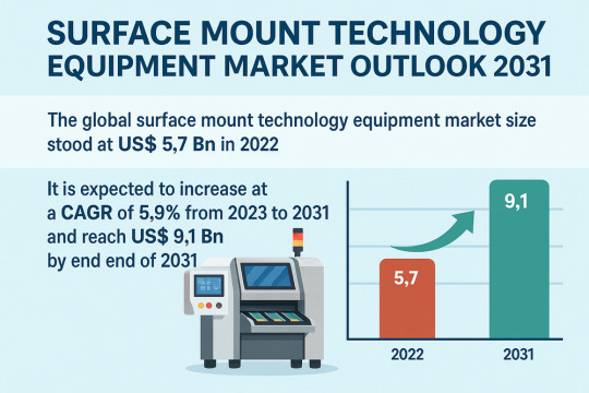
Miniaturized Components Boost Global SMT Equipment Market Demand
The global surface mount technology (SMT) equipment market is poised for substantial growth over the coming decade. Valued at USD 5.7 Bn in 2022, the market is projected to advance at a compound annual growth rate (CAGR) of 5.9% between 2023 and 2031, ultimately reaching USD 9.1 Bn by 2031. SMT equipment plays a critical role in the electronics manufacturing industry by enabling efficient, high-speed, and reliable assembly of surface-mounted components on printed circuit boards (PCBs). The widespread integration of miniaturized and high-performance electronics in consumer devices, automotive systems, telecommunications infrastructure, and industrial automation is significantly driving the adoption of SMT equipment.
Market Drivers & Trends
One of the major drivers of the SMT equipment market is the increasing demand for compact and lightweight electronic devices. With consumer electronics becoming smaller and more multifunctional, the need for advanced SMT machines capable of precise, high-speed placement of components has grown exponentially.
The ongoing shift toward Industry 4.0 and smart manufacturing is also influencing SMT equipment trends. Manufacturers are now integrating artificial intelligence (AI), robotics, and IoT-enabled systems into their production lines to boost efficiency and reduce defects. This trend is reshaping the traditional SMT landscape and encouraging investments in intelligent SMT lines with real-time monitoring and self-correction capabilities.
Additionally, the proliferation of electric vehicles (EVs) and advanced driver-assistance systems (ADAS) is generating new opportunities for SMT equipment manufacturers, particularly in the automotive electronics segment.
Latest Market Trends
Several trends are shaping the SMT equipment market today:
Integration of AI and machine learning in SMT systems to enhance placement accuracy and reduce human intervention.
Adoption of 3D inspection systems for quality control, ensuring higher yield rates and better defect detection.
Expansion of flexible and hybrid SMT lines to accommodate varying production volumes and product types.
Sustainability-focused designs, such as energy-efficient reflow ovens and lead-free soldering systems, are gaining traction amid rising environmental concerns.
These trends are not only boosting productivity but are also redefining customer expectations and pushing market players toward more adaptive and future-ready solutions.
Analysis of Key Players
The surface mount technology equipment industry is consolidated with the presence of a few players holding major market share. Leading manufacturers are following the latest surface mount technology equipment market trends and engaging in new product launches and mergers & acquisitions to consolidate their presence in the global market.
Dou Yee Enterprises (S) Pte. Ltd., JUTZE Intelligence Technology Co., Ltd., Koh Young Technology, Mirtech, Nordson Corporation, Omron Corporation, PARMI Corporation, Saki Corporation, Test Research, Inc., Vi Technology (Mycronic AB), Viscom AG, Vitrox Corporation, and Yamaha Motor Co., Ltd. are a few notable players that offer inspection equipment. While ASML Holding, N.V., Fuji Machine Mfg. Co., Ltd., Hitachi, Ltd., Juki Corporation, KLA-Tencor Corporation, Koh Young Technology, Mycronic AB, Nordson Corporation, Orbotech Ltd., Panasonic Corporation, PARMI Corp., Test Research, Inc., and Yamaha Motor Co., Ltd. are key notable players offering surface mount technology equipment.
Recent Developments
The past few years have seen a wave of strategic developments in the SMT equipment market:
ASMPT introduced a new line of modular SMT systems featuring AI-assisted analytics to optimize throughput.
Panasonic unveiled a next-gen placement machine with enhanced component recognition and autonomous calibration features.
Witte Technology GmbH expanded its European manufacturing facility to increase capacity and meet rising global demand.
Several players have formed partnerships with automotive and telecom firms to tailor SMT solutions for specific industry requirements, such as 5G infrastructure and EV component manufacturing.
Download to explore critical insights from our Report in this sample - https://www.transparencymarketresearch.com/sample/sample.php?flag=S&rep_id=5516
Market Opportunities
Numerous opportunities lie ahead for stakeholders in the SMT equipment space:
Growing electronics manufacturing services (EMS) sector in Asia-Pacific, particularly in countries like China, Vietnam, and India, is creating demand for scalable SMT systems.
The rise of smart wearables and IoT devices presents a growing segment for compact SMT solutions.
High-reliability applications in aerospace, defense, and medical electronics require advanced SMT capabilities, opening niche but profitable markets.
Government incentives in semiconductor and electronics manufacturing across various regions are encouraging infrastructure development and equipment procurement.
Future Outlook
Looking forward, the SMT equipment market is set to evolve in alignment with global digitization and electrification trends. As AI and predictive maintenance become standard in manufacturing environments, the integration of such capabilities in SMT systems will become a key differentiator. Additionally, geopolitical shifts and supply chain restructuring are expected to drive investments in localized manufacturing, fueling SMT equipment demand in emerging markets.
The future of the SMT equipment market will be shaped by technological agility, customization, and sustainability all critical to addressing the dynamic needs of modern electronics manufacturing.
Market Segmentation
The SMT equipment market can be segmented based on:
Equipment Type:
Placement Equipment
Inspection Equipment
Soldering Equipment
Screen Printing Equipment
Cleaning Equipment
Application:
Consumer Electronics
Automotive
Industrial Electronics
Telecommunications
Medical Devices
Aerospace & Defense
End-user:
OEMs (Original Equipment Manufacturers)
EMS Providers
This segmentation highlights the market’s diverse application base and underscores the necessity for flexible and tailored SMT solutions.
Regional Insights
Asia-Pacific dominates the global SMT equipment market, driven by a robust manufacturing ecosystem, especially in China, Japan, and South Korea. The region is expected to remain a powerhouse throughout the forecast period.
North America is witnessing increasing demand due to reshoring efforts and innovations in automotive and medical electronics.
Europe, led by Germany and the UK, is focusing on high-precision SMT systems for automotive and industrial applications.
Latin America and the Middle East & Africa are emerging markets with growing infrastructure and electronics demand, albeit at a relatively slower pace.
Why Buy This Report?
This comprehensive market research report offers:
In-depth analysis of current and future market trends
Thorough competitive landscape assessment including company profiles and market share
Detailed segmentation and regional breakdowns
Insights into technological innovations and investment opportunities
Strategic recommendations for stakeholders, investors, and policymakers
Whether you are a market entrant, investor, OEM, or EMS provider, this report serves as a crucial tool for making informed business decisions.
Explore Latest Research Reports by Transparency Market Research: GPS Tracking Device Market: https://www.transparencymarketresearch.com/gps-tracking-device-market.html
E-Beam Wafer Inspection System Market: https://www.transparencymarketresearch.com/e-beam-wafer-inspection-system-market.html
Filtered Connectors Market: https://www.transparencymarketresearch.com/filtered-connectors-market.html
Commercial Security Systems Market: https://www.transparencymarketresearch.com/commercial-security-systems-market.html
About Transparency Market Research Transparency Market Research, a global market research company registered at Wilmington, Delaware, United States, provides custom research and consulting services. Our exclusive blend of quantitative forecasting and trends analysis provides forward-looking insights for thousands of decision makers. Our experienced team of Analysts, Researchers, and Consultants use proprietary data sources and various tools & techniques to gather and analyses information. Our data repository is continuously updated and revised by a team of research experts, so that it always reflects the latest trends and information. With a broad research and analysis capability, Transparency Market Research employs rigorous primary and secondary research techniques in developing distinctive data sets and research material for business reports. Contact: Transparency Market Research Inc. CORPORATE HEADQUARTER DOWNTOWN, 1000 N. West Street, Suite 1200, Wilmington, Delaware 19801 USA Tel: +1-518-618-1030 USA - Canada Toll Free: 866-552-3453 Website: https://www.transparencymarketresearch.com Email: [email protected]
0 notes
Text
0 notes
Text
The Future of Electronics Starts with the PCB — And It’s Being Built in India
Behind every smartphone, drone, EV, or IoT device, there’s one common core: the Printed Circuit Board (PCB). Often overlooked, yet absolutely essential, PCBs are the unsung heroes of the modern world.
If you're developing a new tech product, here's something you need to know: India is quickly becoming the global hub for PCB fabrication and assembly.
What is PCB Fabrication?
PCB fabrication is the process of manufacturing the actual circuit board — the foundation that holds and connects all electronic components. It involves precise steps such as:
Layering copper and substrate materials
Etching pathways
Drilling and plating vias
Applying solder masks and silkscreens
Electrical testing and inspection
A top-tier PCB fabrication company in India provides quality manufacturing that meets international standards, all while remaining cost-effective and scalable for startups or mass production.
What is PCB Assembly?
Once the board is fabricated, it’s time for PCB assembly — the process of placing and soldering components like resistors, capacitors, and microcontrollers onto the board. Assembly involves:
Surface Mount Technology (SMT)
Through-Hole Technology (THT)
Component placement automation
Reflow soldering and inspection
Functional testing and quality control
A reliable PCB assembly company in India will ensure your product functions flawlessly from the start, and can scale as your demand grows.
Why India is the Smart Choice
Here’s why companies across the globe are turning to India for their PCB needs:
1. Skilled Engineering Talent India has a vast pool of trained professionals with deep expertise in electronics manufacturing and design.
2. State-of-the-Art Facilities Leading PCB companies in India operate world-class cleanrooms and production lines equipped with high-speed SMT machines and automated testing tools.
3. Competitive Costs Get high-quality PCBs at globally competitive prices — without compromising reliability or delivery speed.
4. Fast Prototyping and Mass Production Indian companies support both small-batch prototyping and high-volume orders with quick turnaround times.
5. Compliance and Quality Most Indian manufacturers follow international standards (ISO, IPC, RoHS), ensuring your boards are ready for export or high-performance applications.
Who Needs a PCB Partner in India?
If you're building or scaling a product in any of these industries:
Consumer Electronics
Industrial Automation
Electric Vehicles
Medical Devices
Aerospace and Defense
Telecommunications
IoT and Wearables
Then partnering with a PCB fabrication and assembly company in India could dramatically reduce your time-to-market while keeping production costs under control.
Final Thoughts
The electronics industry is evolving fast. To stay competitive, you need speed, precision, and reliability — right from the circuit board up. By working with a top-tier PCB fabrication or assembly company in India, you're investing in a foundation that’s built for innovation.
India isn't just manufacturing PCBs. It's powering the next generation of technology
#PCB#ElectronicsManufacturing#TechStartup#ProductDesign#PCBIndia#PCBAssembly#HardwareStartup#Innovation#ElectronicsEngineering#PCBFabrication#IndustrialDesign#MadeInIndia
1 note
·
View note
Text
What Is a Surface-Mount Reflow Oven and Its Importance in Electronics?
In the dynamic realm of electronics manufacturing, precision and efficiency are critical. The surface-mount reflow oven is a cornerstone of this industry, enabling the reliable soldering of electronic components onto printed circuit boards (PCBs) through a meticulously controlled heating and cooling process. Unlike traditional through-hole soldering, which involves inserting component leads into PCB holes, surface-mount technology (SMT) places components directly on the PCB surface. The surface-mount reflow oven facilitates this process with unmatched accuracy. This comprehensive guide delves into the functionality, components, processes, and pivotal role of the surface-mount reflow oven in modern electronics assembly, highlighting its significance in producing high-quality devices.

What Are the Core Components of a Surface-Mount Reflow Oven?
The surface-mount reflow oven is a sophisticated machine designed to execute precise soldering for surface-mount components. Its design incorporates several key components that ensure seamless operation during the soldering process:
Conveyor System: The surface-mount reflow oven features a conveyor belt or chain that moves PCBs through various zones at a controlled speed, ensuring uniform exposure to heating and cooling phases, which is essential for consistent results.
Heating Zones: A surface-mount reflow oven typically includes multiple heating zones, each equipped with heating elements (e.g., infrared or convection) and precise temperature sensors. These zones gradually increase the PCB’s temperature to activate solder paste and form strong bonds.
Cooling Zones: After heating, the surface-mount reflow oven’s cooling zones lower the PCB’s temperature rapidly to solidify solder joints, preventing thermal damage and ensuring durable connections.
Control System: Advanced surface-mount reflow ovens are equipped with intelligent control systems that monitor and adjust parameters like temperature profiles, conveyor speed, and airflow, optimizing the soldering process for diverse PCB designs.
These components make the surface-mount reflow oven a vital tool for achieving reliable and repeatable soldering outcomes in electronics manufacturing.
How Does the Surface-Mount Reflow Oven Process Work?
The soldering process in a surface-mount reflow oven is a critical step in surface-mount technology, ensuring components are securely bonded to PCBs. The surface-mount reflow oven orchestrates a series of carefully controlled steps to achieve this. Below is a detailed overview of the process, reflecting current industry standards:
Solder Paste Application: Before components are placed, solder paste—a blend of solder particles and flux—is applied to PCB solder pads using stencil printing or jet printing. In the surface-mount reflow oven, this paste serves as an adhesive and facilitates solder joint formation.
Component Placement: Automated pick-and-place machines position surface-mount components onto the solder paste deposits with high precision, a crucial step before entering the surface-mount reflow oven. Accurate placement ensures alignment with the PCB’s layout.
Preheating Phase: The PCB enters the surface-mount reflow oven’s preheating zone, where temperatures rise gradually to 150–200°C (302–392°F). This phase removes moisture, activates flux, and prepares the assembly for soldering without thermal shock.
Ramp-Up Phase: In the surface-mount reflow oven, the ramp-up phase follows, with temperatures increasing to a peak of 220–260°C (428–500°F), depending on the solder alloy (e.g., lead-free SAC305 or leaded solder). The ramp rate is controlled to avoid component stress.
Reflow Phase: At peak temperature, the solder paste melts in the surface-mount reflow oven, transitioning to a liquid state. The flux cleans metal surfaces, enabling strong solder joints between component leads and PCB pads. This phase lasts 20–60 seconds for optimal bonding.
Cooling Phase: The surface-mount reflow oven’s cooling zone gradually reduces temperatures to solidify solder joints, preventing brittle connections and minimizing thermal stress for reliable assemblies.
Inspection: After cooling in the surface-mount reflow oven, PCBs undergo inspection using automated optical inspection (AOI), X-ray imaging, or in-circuit testing to detect defects like solder bridges or misaligned components.
Cleaning (Optional): Some PCBs processed in a surface-mount reflow oven are cleaned to remove flux residues, depending on the flux type. No-clean fluxes reduce this need in many modern applications.
Functional Testing: Finally, PCBs are tested to ensure all components function correctly, confirming the efficacy of the surface-mount reflow oven process.
The surface-mount reflow oven’s precise execution of these steps ensures high-quality PCB assemblies.
What Temperature Profiles Are Used in a Surface-Mount Reflow Oven?
The surface-mount reflow oven operates with specific temperature profiles tailored to the solder alloy and PCB requirements. Below are the typical temperature ranges in a surface-mount reflow oven, based on industry standards:
Preheating Zone: 150–200°C (302–392°F). This zone in the surface-mount reflow oven prepares the PCB by removing moisture and preventing thermal shock.
Ramp-Up Zone: Temperatures rise to a peak of 220–260°C (428–500°F) in the surface-mount reflow oven, with lead-free alloys requiring higher peaks (245–260°C).
Reflow Zone: The surface-mount reflow oven maintains the peak temperature for 20–60 seconds to ensure complete solder melting and joint formation.
Cooling Zone: The surface-mount reflow oven gradually lowers temperatures to solidify solder joints, ensuring reliability and minimizing stress.
Sophisticated surface-mount reflow ovens use sensors and software to customize these profiles, adhering to standards like IPC/JEDEC J-STD-020 and accommodating modern component sensitivities.
Why Is the Surface-Mount Reflow Oven Essential in Electronics Manufacturing?
The surface-mount reflow oven is indispensable in electronics manufacturing for several compelling reasons:
Precision and Consistency: The surface-mount reflow oven ensures precise temperature control, producing uniform solder joints critical for high-reliability applications like medical devices and automotive electronics.
High Efficiency: By automating soldering, the surface-mount reflow oven boosts throughput, reducing labor costs and time compared to manual methods, making it ideal for high-volume production.
Support for Miniaturization: The surface-mount reflow oven enables precise soldering of tiny components (e.g., 0201 resistors, micro-BGAs), supporting compact devices like smartphones and wearables.
Versatility: The surface-mount reflow oven accommodates various solder alloys and PCB types, from flexible to rigid boards, catering to diverse manufacturing needs.
Companies like CHENGLIANKAIDA Technology Co., Ltd., based in Beijing, enhance related fields like semiconductor device packaging, contributing to the precision and innovation seen in surface-mount reflow oven applications. Their work underscores the industry’s push toward advanced manufacturing solutions.
What Lies Ahead for Surface-Mount Reflow Ovens?
The future of the surface-mount reflow oven is shaped by emerging technologies like 5G, artificial intelligence, and electric vehicles, which demand greater precision and thermal control. Innovations such as nitrogen-based surface-mount reflow ovens, which minimize oxidation, and hybrid models combining convection and infrared heating are gaining popularity. Additionally, Industry 4.0 integration—featuring real-time monitoring and AI-driven optimization—transforms the surface-mount reflow oven into a smart, connected system, improving yields and reducing downtime.
Conclusion
The surface-mount reflow oven is a linchpin of modern electronics manufacturing, enabling precise and efficient soldering of components onto PCBs. By understanding its components, processes, and significance, manufacturers can leverage the surface-mount reflow oven to meet the demands of compact, high-performance electronics. As technology evolves, the surface-mount reflow oven will continue to drive innovation, ensuring the production of reliable, cutting-edge devices.
#asexual#easter#margot robbie#michael cera#across the spiderverse#artists on tumblr#donald trump#rwby#barbie#ryan gosling
0 notes