#Synopsys RISC-V
Explore tagged Tumblr posts
Visit Tumblr Blog
Explore Tumblr blogs with no restrictions, modern design and the best experience.
Last Seen Tumblr Blogs


Fun Fact
The KCSC sent more than 20K requests to delete posts related to prostitution and porn to Tumblr from January to June 2017.
Text
Codasip seeks buyer amid growing pressure in RISC-V processor market
July 2, 2025 /SemiMedia/ — Germany-based RISC-V processor specialist Codasip has been put up for sale, as the company’s board seeks to complete a transaction within three months, aiming to address mounting competition and funding pressures in the open-architecture CPU sector. Under CEO Ron Black’s leadership, Codasip is exploring options including a full sale or business unit spin-offs. The…
#automotive-grade processor#Codasip sale#EDA tool#electronic components news#Electronic components supplier#Electronic parts supplier#embedded CPU#RISC-V processor#SiFive#Synopsys RISC-V
0 notes
Text
youtube
0 notes
Text
South Korea Semiconductor IP Market is driven by AI device demand

Semiconductor intellectual property (IP) cores serve as pre-designed building blocks for complex system-on-chip (SoC) architectures, enabling chip designers to integrate high-performance processor, memory, interface, and encryption modules without investing in ground-up development. These cores accelerate time-to-market, reduce design costs, and enhance power efficiency, making them essential in consumer electronics, automotive systems, and industrial IoT applications.
As chip geometries shrink and functional integration grows, the need for robust verification environments and standardized IP becomes paramount. The market research highlights that adoption of RISC-V, ARM, and custom IP solutions drives product differentiation and competitiveness. Ongoing developments in low-power design, secure processing, and AI accelerators further expand South Korea Semiconductor IP Market opportunities by enabling edge computing and 5G device support. Continuous innovation in packaging and heterogeneous integration underscores evolving market trends, while strategic alliances and licensing agreements shape market dynamics.
The South Korea Semiconductor IP Market is estimated to be valued at USD 2.16 Bn in 2025 and is expected to reach USD 6.68 Bn by 2032, growing at a compound annual growth rate (CAGR) of 17.5% from 2025 to 2032. Key Takeaways
Key players operating in the South Korea Semiconductor IP Market are:
-Arm Holdings
-Synopsys, Inc.
-Cadence Design Systems, Inc.
-Imagination Technologies Limited
-Lattice Semiconductor These market companies hold significant industry share through extensive IP libraries spanning CPUs, GPUs, interconnects, and security modules. Arm Holdings continues to lead with versatile Cortex-series cores, while Synopsys and Cadence bolster their portfolios with advanced verification and custom IP tooling. Imagination Technologies focuses on graphics and neural processing IP, and Lattice Semiconductor addresses low-power FPGA-integrated IP. Collaborative research and licensing agreements among these players foster innovation and help maintain competitive market positions.
‣ Get More Insights On: South Korea Semiconductor IP Market
‣ Get this Report in Japanese Language: 韓国の半導体IP市場
‣ Get this Report in Korean Language: 한국반도체IP시장
0 notes
Text
倪光南院士:开源RISC-V是芯片产业变革的新引擎
2月28日,由达摩院举办的2025玄铁RISC-V生态大会在北京举行,中国科学院软件研究所、国网南瑞、普华基础软件、经纬恒润、新思科技(Synopsys)、Cadence、西门子EDA等全球数百家企业及机构齐聚一堂。
0 notes
Link
Synopsys announced its plans for expanding its processor intellectual property portfolio with the new RISC-V ARC-V family. #AI #ML #Automation
0 notes
Text
Synopsys joins RISC-V party with trio of embedded core designs
http://securitytc.com/SyWDGw
0 notes
Text
SoCs for Edge Computing- ASIC/SoC Physical Design- SoC Design Verification
Today, I am eager to report the dispatch of Open Five, an independent and independent custom silicon specialty unit of SiFive, Inc. Open Five is arrangement driven and remarkably situated to plan processor skeptic SoCs for edge computing and convey great silicon. The interest in area explicit silicon and responsibility-centered design is driven by a few key elements. Broadly useful processors used to be the workhorses for most of registering errands.
Open Five is a solution-centric silicon company that is uniquely positioned to design processor agnostic SoC architecture. With semiconductor cost expanding, and the finish of Den nard scaling, universally useful processors have become very eager for power, and execution increments are elusive from process innovation alone – engineering assumes a key part in a responsibility speed increase.
With customizable and differentiated IP, Open Five develops domain-specific SoC architecture based on high-performance, highly-efficient, cost-optimized IP to deliver scalable, optimized, differentiated silicon.
Area explicit or responsibility cantered silicon empowers the practical, versatile items wanted by innovation organizations that need to claim their Open Five is worked around the equilibrium of silicon skill and adjustable IP, including an engaged arrangement of SoC IP to empower key plan highlights.
Open Five offers end-to-end expertise in Architecture, ASIC/SoC Physical Design, Design Implementation, Software, Silicon Validation, and Manufacturing to deliver high-quality silicon.
Open Five’s high-level plan approaches to empower the utilization of driving edge foundry hubs, including 5nm, with 2.5D bundling innovation, to construct Artificial Intelligence, Edge Computing, HPC, and Networking arrangements. Interconnect IP for cutting-edge heterogeneous chiplet-style items.
Open Five’s expansive industry skill empowers us to foster SoCs with an assortment of processor centers, including RISC-V design just as processors from Arm, Cadence, CEVA, and Synopsys. This ISA-rationalist and open methodology will assist with speeding up the reception of RISC-V in new plans, as chip architects search for the best IP for each useful square inside their SoC plans.
The open, free RISC-V ISA is the reason for the SiFive Core IP portfolio – the broadest in the business. SiFive centers, alongside other RISC-V-based centers, and centers from other Isa's, can make a heterogeneous blend of utilization, installed, and microcontrollers to empower an advanced area explicit plan. We're staggeringly amped up for the chance that space explicit silicon offers Open Five clients in their cutting-edge items.
With a legacy and skill crossing over 15 years, over 150M units delivered, and over 350 tape-outs, Open Five’s start to finish ability in Architecture, Design Implementation, Software, Silicon Validation, and Manufacturing empowers the plan and conveyance of excellent silicon, with first-time-right outcomes.
For more data on the arrangement of IP and silicon arrangements, Open Five can accommodate your new in an upward direction incorporated, separated plan project, if it's not too much trouble, interface with us here. All brand names referred to in this have a place with their separate organizations. s a senior specialist RTL plan, you will be working in SoC plan, subsystem plan.
You will be liable for the microarchitecture and creating micro architecture archives. You will be working with check groups on accomplishing the region, power, and execution objectives. You will be supporting actual plan groups, confirmation groups, programming groups, and FPGA groups to guarantee to have a great SoC subsystem for the clients and guarantee effective takeout.
0 notes
Text
Lattice Semiconductor Launches New FPGA For Cyber-Resilient Systems
New Post has been published on https://perfectirishgifts.com/lattice-semiconductor-launches-new-fpga-for-cyber-resilient-systems/
Lattice Semiconductor Launches New FPGA For Cyber-Resilient Systems
Earlier this week, Lattice Semiconductor announced its newest product built on the Lattice Nexus FPGA platform, the Mach-NX. The Mach-NX FPGA product family addresses the growing threat of firmware hacking attempts on systems, leading to the loss of customer IP. Moor Insights & Strategy have written a lot about this growing threat, funded by nation-states with “as a service” business models.
As bad actors continue to attack firmware, companies like Lattice Semiconductor need to constantly be upping its games to enable their customers to create cyber-resilient systems. Enter a new FPGA from Lattice. The Mach-NX is a high performance, low power FPGA product family aimed at dynamic, real-time, and end-to-end platform protection. This launch is the next logical step for Lattice on its low power FPGA journey and marks the third Nexus launch in a year. The company is uniquely positioning itself as a leader, if not the leader in low power FPGA security solutions, and this launch helps reinforce that.
Lattice has been delivering new security-focused FPGAs at a faster cadence than we are used to. Since FPGAs are incredibly flexible, it also gives Lattice the ability to expand its presence into different markets that need programmable security solutions. In recent memory, Lattice launched CrossLink-NX in late 2019, Certus-NX this past summer, and now Mach-NX. You can read my full write up on the Certus-NX launch here. Lattice was ambitious when it promised to speed up its launch cadence by 3x, and it has done just that in 2020. The company seems hyper focused on low power FPGA dominance as 2020 comes to an end, and its future seems bright.
Lattice Semiconductor Mach NX
As hackers continue to attack firmware vulnerabilities with nation-state budgets and “as a service” models, companies need a flexible, secure solution that can adapt and serve different industries and applications. That problem is the exact reason that Lattice developed its new security-focused FPGA, Mach-NX. The new Mach-NX FPGA family will build on the previous product, the Lattice MachXO3D family. The new Mach-NX product family will address future server platforms, computing, communications, industrial, and automotive systems. Like other Lattice Nexus products, the new Mach-NX FPGA will utilize the same 28 nm FD-SOI fab process. While not a bleeding edge geometry, the specialized FD-SOI process technology allows Lattice to deliver extremely energy-efficient solutions without sacrificing performance. I also believe this solution is much smaller than competing solutions. High performance while maintaining low power matters a lot when you consider that traditionally high-density FPGAs trade power for size. I’ve talked enough about application and product introduction; let’s get into the nuts and bolts of the Mach-NX.
I listed the new features verbatim for the Mach-NX FPGA products from Lattice’s announcement.
Up to 8.4K LC of user logic, 2669kbits of user flash memory, and dual boot flash feature.
Up to 379 programmable I/O supporting 1.2/1.5/1.8/2.5/3.3 I/O voltages.
Secure enclave supports 384-bit cryptography, including SHA, HMAC, and ECC.
Lattice Semiconductor Mach-NX
The first goal of a security solution is establishing a Hardware Root of Trust upon boot, which the Mach-NX does. The Mach-NX FPGAs also give users real-time performance against security risks with real-time SPI monitoring. According to Lattice, the Mach-NX FPGAs can again recover firmware within microseconds, where other FPGAs can take 100s of milliseconds or even minutes to recover firmware.
The 384-bit encryption is a significant security upgrade from the 256-bit encryption we saw with the last generation products. This security level becomes essential, especially when considering the longevity of end products that would adopt the Mach-NX, which could be up to 10 years. As the number of attack vectors and cyber-attacks is increasing rapidly, security solutions need to adapt and become harder to hack. Another value that customers get from implementing Mach-NX FPGAs is customizing solutions specifically for their applications and use. Customers will be able to configure their FPGAs’ security using RISC-V and Lattice’s Propel Design Environment. I admire the way Lattice is positioning its Mach-NX solution as a first on, last-off, real-time, fully customizable solution for the customer’s unique needs. When you pair these solutions with Lattice’s security service, SupplyGuard, a customer’s system can be protected throughout the product life cycle’s duration.
Lattice Semiconductor Mach-NX
Wrapping up
All in all, Lattice’s new Mach-NX looks to deliver on its core value proposition and extends the capabilities of Lattice’s previous generation of secure control FPGAs. Attack vectors and hackers will continually evolve their attack methods, and as those change, I believe s Lattice’s solutions will volve to address those methods.
Since this time last year, Lattice has launched three FPGA product families built on its Lattice Nexus FPGA platform with no signs of slowing down. If you recall, since CEO Jim Anderson took the helm Lattice looks to have generated a tremendous amount of momentum with Lattice Nexus, as further reinforced by the launch of Mach-NX. Add to that the work the company has put in to round out its offerings with application-focused solutions stacks and software design tools, and it’s clear they are laser-focused on delivering on the promise of low power programmable leadership.
Note: Moor Insights & Strategy writers and editors may have contributed to this article.
Moor Insights & Strategy, like all research and analyst firms, provides or has provided paid research, analysis, advising, or consulting to many high-tech companies in the industry, including 8×8, Advanced Micro Devices, Amazon, Applied Micro, ARM, Aruba Networks, AT&T, AWS, A-10 Strategies, Bitfusion, Blaize, Box, Broadcom, Calix, Cisco Systems, Clear Software, Cloudera, Clumio, Cognitive Systems, CompuCom, Dell, Dell EMC, Dell Technologies, Diablo Technologies, Digital Optics, Dreamchain, Echelon, Ericsson, Extreme Networks, Flex, Foxconn, Frame (now VMware), Fujitsu, Gen Z Consortium, Glue Networks, GlobalFoundries, Google (Nest-Revolve), Google Cloud, HP Inc., Hewlett Packard Enterprise, Honeywell, Huawei Technologies, IBM, Ion VR, Inseego, Infosys, Intel, Interdigital, Jabil Circuit, Konica Minolta, Lattice Semiconductor, Lenovo, Linux Foundation, MapBox, Marvell, Mavenir, Marseille Inc, Mayfair Equity, Meraki (Cisco), Mesophere, Microsoft, Mojo Networks, National Instruments, NetApp, Nightwatch, NOKIA (Alcatel-Lucent), Nortek, Novumind, NVIDIA, Nuvia, ON Semiconductor, ONUG, OpenStack Foundation, Oracle, Poly, Panasas, Peraso, Pexip, Pixelworks, Plume Design, Poly, Portworx, Pure Storage, Qualcomm, Rackspace, Rambus, Rayvolt E-Bikes, Red Hat, Residio, Samsung Electronics, SAP, SAS, Scale Computing, Schneider Electric, Silver Peak, SONY, Springpath, Spirent, Splunk, Sprint, Stratus Technologies, Symantec, Synaptics, Syniverse, Synopsys, Tanium, TE Connectivity, TensTorrent, Tobii Technology, T-Mobile, Twitter, Unity Technologies, UiPath, Verizon Communications, Vidyo, VMware, Wave Computing, Wellsmith, Xilinx, Zebra, Zededa, and Zoho which may be cited in blogs and research.
From Cloud in Perfectirishgifts
0 notes
Text
中國如何在開源芯片領域找到突破口? RISC-V 會是一個絕佳機會
在6 月27 日至29 日由國際測試委員會(BenchCouncil)主辦,國家超級計算深圳中心、中科曙光等單位共同承辦的第六屆世界智能計算機大會(BenchCouncil 2019)上,包雲崗研究員更是組織了一場以“開源芯片”為主題的分論壇,邀請了RISC-V 基金會中國委員會主席方之熙、中國RISC-V 產業聯盟理事長戴偉民、北京大學信息科學技術學院高能效計算與應用中心助理研究員羅國傑、中國科學院計算技術研究所在讀博士生餘子濠一眾專家學者,從各個維度共同探討以RISC-V 為代表的開源芯片目前的現狀和未來,以及中國該如何在開源芯片領域找到突破口。
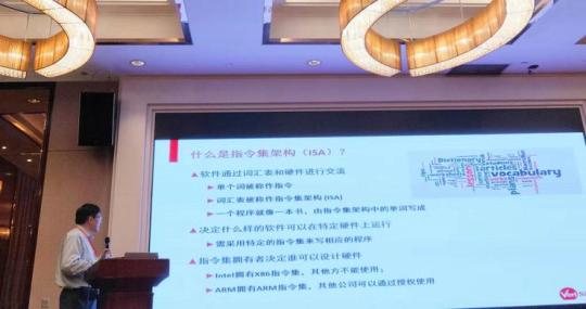
RISC-V 基金會中國委員會主席、前英特爾副總裁方之熙博士作為第一位出場嘉賓,帶來了主題為《為什麼說 RISC-V 是微處理器的一場革命》的演講報告。他基於微處理器的發展現狀以及目前面臨的一些問題,探討了 RISC-V 的優勢以及給微處理器領域帶來的革命性影響,並從哲學層面分享了其對於微處理器未來發展的看法。
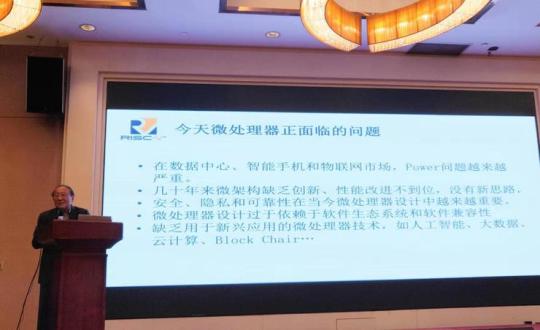
RISC-V 基金會中國委員會主席方之熙
首先,方之熙博士指出計算領域的現狀是: 99% 的雲計算基於 Inter x86 指令集架構,99% 的邊緣計算使用 RISC 指令集架構,75% 的計算採用的是 ARM(高級 RISC 機器)。而微處理器目前則面臨著幾大主要問題,包括:第一,在數據中心、智能手機和物聯網市場,功耗問題越來越嚴重;第二,幾十年來微架構缺乏創新、性能改進不到位、沒有新思路;第三,安全、隱私和可靠性在當今微處理器設計中越來越重要;第四,微處理器設計過於依賴軟件生態系統和軟件的兼容性;第五,目前缺乏用於新興應用的微處理器技術,例如人工智能、大數據、雲計算以及區塊鍊等。
而 RISC-V 的出現則為微處理器領域帶來了革命性的變化。作為開放源碼硬件指令集體系架構(ISA),自2010 年誕生於加州大學伯克利分校的RISC-V ,以其簡單、穩定,完全開源並且免費的特點,同時可以將基準指令和擴展指令分開從而能夠通過擴展指令做定制化的模塊和擴展,為芯片設計迎來了新時代。
最後,他以愛因斯坦的一句“Not everything that can be counted counts, and not everything that counts can be counted(並不是每一件能夠算出來的東西,都是有意義的;也並不是每一件有意義的東西,都能夠被計算出來)”表達了他對於微處理器未來發展的看法。同時,他也表示,“Future can't be predicted,but it can be created”,雖然我們很難確切地“預測”微處理器的未來,但是我們可以為該領域“創造”更好的未來。
第二位出場的是中國 RISC-V 產業聯盟理事長戴偉民博士,他的演講主題是《RISC-V: 中國集成電路產業的歷史機遇》。他從 RISC-V 的發展歷程出發,分享了中國在開源芯片領域未來的發展機遇。
中國 RISC-V 產業聯盟理事長戴偉民
一開始,他指出,由於晶體管、功耗等沒有太大改進空間,並且在2003 年就已經從單一抵消處理器(芯片)轉換到了多核高效處理器(芯片),目前只能在專用領域加速器上找到突破口,即開發出能夠在某幾個特定任務上實現高效執行,同時能夠提高計算單位功耗性能的芯片。
而 RISC(精簡指令集計算機)相對於復雜指令而言,不僅在指令讀取方面簡單 25%,在速度和功耗上也有其獨特的優勢,如今最具代表性的成果便是 RISC-V。對此,戴偉民博士向大家展示了 RISC-V(以及在中國)的發展歷程:
1979 年美國加州大學柏克利分校的 David Patterson 教授提出了 RISC 的概念;
2010 年美國加州大學柏克利分校研究團隊推出 RISC-V 指令集;
2014 年,正式發布第一版用戶手冊;2015 年,RISC-V 基金會成立,吸引了全世界 150 多家企業和科研機構的加入;
2016 年,RISC-V 成為印度的事實國家指令集,同時美國、歐洲和俄羅斯等國家也開始全國推行;
2018 年,RISC-V 在中國逐步商業化;
2018 年 9 月 20 日,中國 RISC-V 產業聯盟正式成立。
他表示,中國實際上基本上所有類型的CPU 都有了,但是敏銳度還是比較滯後,而要想在未來掌握CPU 發展的主動權,需要實現四個層次——自主、可控、繁榮和創新,而RISC-V 所具有的特性恰恰就能實現這四個層次,符合人工智能異構計算的發展需要,因而也為中國在該領域未來的發展提供了不可多得的歷史機遇。
在這樣的背景下,前有中國RISC-V 產業聯盟於2018 年10 月正式成立,聚焦了100 多家會員單位;後有清華和伯克利攜手在6 月12 日成立RISC-V 國際開源實驗室( RISC International Open Source,RIOS),將瞄準世界CPU 產業戰略發展新方向和粵港澳大灣區產業創新需求,聚焦於RISC-V 開源指令集CPU 研究領域開展研究,建設以深圳為根節點的RISC- V 全球創新網絡,並最終推動全球RISC-V 技術的工業化進程和軟硬件生態建設。
緊接著,由本次論壇的主持人包雲崗研究員帶來《The Four Steps to Open-Source Chip Ecosystem》的主題演講。他基於自身轉向 RISC-V 研究的經歷和經驗,分享了自己對於開源芯片領域的一些思考以及如何構建開源芯片生態的觀點。
中科院計算所研究員包雲崗
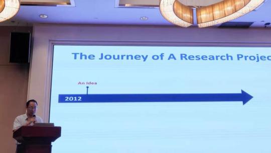
包雲崗研究員首先分享了他之所以走向開源芯片這一研究領域的背景:2012 年開始,為了驗證關於改進芯片體系結構的一個想法——標籤化體系結構,所在團隊一開始在Sparc T1 上進行了嘗試,但是沒有成功驗證該想法;半年後,經過探索終於在MicroBlaze 上驗證了想法,但是無法實現開源和流片;因而最終轉向RSIC-V ,並最終推出了“標籤化RISC-V”。而在這個過程中,包雲崗研究員在包括 RISC-V 在內的開源芯片領域積累了很多經驗,也有很多思考。
他指出,對於軟件開發而言,開源一方面能夠降低創新門檻,另一方面也能夠增強研究者的自主可控能力。然而芯片開發則與軟件開發完全不同,其面臨著開發門檻非常高,只有少部分大公司才能負擔得起,成為創新的巨大阻礙。另外值得注意的是,開源芯片領域現在也面臨非常嚴重的“死鎖”現象:企業不願意進行投入來開源→只能購買高價芯片→通過長時間的驗證來降低風險→反過來又增加了投入→更加不願意投入。因此,降低芯片開發的門檻,意義重大。
而如何將成本降下來呢?包雲崗研究員指出了三個機會:第一,貝爾定律依舊存在,IOT 這一新興產業正在崛起,帶來了新的需求:定制化、更小的尺寸、更低功耗和成本、新的編程模式,同時在製造工藝更加靈活;第二,摩爾定律的終結帶來了機會,芯片工藝成本,尤其是成熟工藝正在指數級下降,而摩爾定律的終結也意味著成熟工藝的生命週期也會變長,成本也不斷下降,帶帶來巨大價值;第三,黃金時代正在來臨,當開源軟件、硬件,新語言,新應用以及雲融合在一起後,就會產生很多新的化學反應。
又如何朝著開源芯片生態發展呢?對此,他認為在這個過程中有四個步驟:第一步是ISA、IP 和Soc 實現開源;第二步是構建語言和EDA 的工具鏈;第三步是降低驗證和仿真的門檻;第四步是具備適配的軟件和編譯器。
“我們現在非常需要一個平台來將這些功能整合起來,我們的願景是 90% 的功能都能通過這個平台實現,而只需要用戶寫 10% 的代碼。”
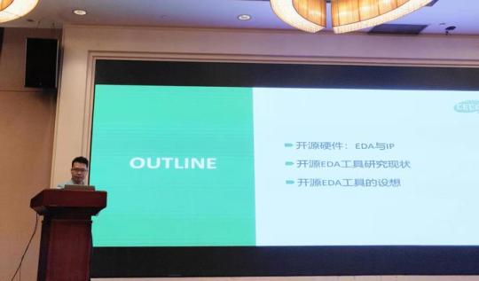
來自北京大學信息科學技術學院高能效計算與應用中心的助理研究員羅國傑博士帶來的演講主題是《開源 EDA 與開源 IP:芯片未來生態的基礎設施》,他主要從開源 EDA 和開源 IP 的關係、開源 EDA 工具的研究現狀以及開源 EDA 工俱生態的設想展開本次演講。
北京大學信息科學技術學院高能效計算與應用中心助理研究員羅國傑
演講一開始,羅國傑博士就指出當前芯片設計困難重重,其中以設計成本為典型,並且目前設計成本也越來越難以跟隨摩爾定律,EDA 軟件許可證、較長的開發週期、開發人員的薪水、計算資源開銷等也成為設計成本中的幾大重要問題。而完整的開源芯片設計的EDA 流程涉及到框架設計、邏輯設計、物理設計以及版圖設計等四大層面,開源要想取得成功也必須是以兼顧性能、功耗和應用領域的高質量(PPA)的開源為前提的。
針對開源EDA 與開源IP 關係,他指出,開源芯片由四個主體部分共同組成:一是完整的芯片,其由開源IP 組成;二是開源IP,它不僅需要core,還需要ddr phy 以及usb、 wifi 等工具;三是開源EDA,其不僅能夠幫助IP 進行設計和驗證,還能幫助IP 實現集成或芯片設計;四是開源編譯器,RSIC-V 便是編譯器和指令集之間的接口。
其中,羅國傑博士重點介紹了EDA 工具的行業現狀:目前僅國外EDA 三大巨頭公司Cadence、Synopsys 及Mentor Graphics 就佔據了全球該行業每年總收入的70%,而中國本土雖然也有自主EDA 軟件,例如華大EDA 和EasyEDA 等產品,做了多年技術積累,並擁有一大批成功用戶案例,但與國外EDA 三大巨頭公司相比,在完整自動化設計流程上存在巨大的技術差異。
而作為全球最大的電子芯片消費市場,我國對於EDA 的需求也是全球最高的,然而在我國目前的EDA 現狀下,我國學術界與工業界也只能廣泛採用國外的EDA 工具——每年用來購買EDA 工具的使用權的花費高達數十億美元。我國自主開源硬件開發 EDA 工具鏈成為急需發展和意義重大的事項。
不僅開源、可靠的 EDA 工具對我國市場有重要意義和研發動力,開源 EDA 工具的定制化也能夠驅動我國新興應用和新興工藝的探索。與此同時,我國面臨的挑戰也十分明顯,包括芯片合計需要連接算法和物理層面,設計眾多複雜的專業知識;發展完整的EDA 工具鏈需要眾多社區的支持和維護;運行大規模設計的EDA 工具需要大量高性能服務器。
最後,羅國傑博士對於如何進一步提升開源EDA 工俱生態提出了三步:一是時限後端整合,解決芯片製造商接口和工具解決開源EDA 與相對閉源製造是數據的矛盾;二是從開源硬件的角度,支持開源IP 的EDA 方法,以及推動開源IP 與EDA 社區的融合;三是建立IP+EDA+開發數據的完善的生態體系,並實現工具和流程的流片驗證。
論壇最後,由中國科學院計算技術研究所在讀博士生餘子濠帶來主題為《基於 Labeled RISC-V 的芯片敏捷開發》的演講。他為大家介紹了降低門檻開發的解決方案——芯片敏捷開發,並從其之前參與的研究項目出發,分享了敏捷開發的優勢以及一些經驗。
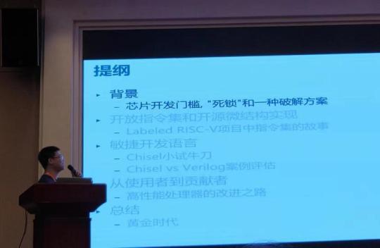
中國科學院計算技術研究所在讀博士生餘子濠
目前,芯片開發需要投入相當的人力和時間才能開展 , 並且具有一定的風險 , 芯片開發的門檻一直居高不下。在這樣的背景下,其中的一個解決方案便是芯片敏捷開發,這種方法能夠有效降低開發成本,不過也需要三個前提條件:一個開放的指令集、一個開源的微架構實現以及一門面向敏捷開發法的設計語言。而加州大學伯克利分校先後設計出的開放指令集RISC-V,並開放的其SoC 實現Rocket Chip 的項目源碼, 以及提出的一門面向敏捷開發的硬件構建語言Chisel 正好就構成了實現芯片敏捷開發的“新三架馬車”。
餘子濠博士之後更是基於中國科學院計算技術研究所在“標籤化 RISC-V”項目開發過程中的若干案例 , 為大家總結了敏捷開發的優勢以及過程中選用工具和語言的經驗:
與傳統開發相比,敏捷開發能在編碼效率提升一個數量級的同時 , 能達到與傳統硬件開發模式相當甚至更優的性能、功耗與面積;
開放又活躍的指令集生態(如 RISC-V)及其開源的微結構設計是推動芯片研發創新的必要條件;
Chisel 的信號整體連接、元編程、面向對象編程以及函數式編程等特性可大幅縮減代碼量、提升代碼可維護性,但同時,Chisel 和後端配合還存在不少問題待改進。
.
from 中國如何在開源芯片領域找到突破口? RISC-V 會是一個絕佳機會 via KKNEWS
0 notes
Text
SiFive’s RISC-V for makers; Arm’s Graviton2; Synopsys’ software integrity success.
SiFive’s RISC-V for makers; Arm’s Graviton2; Synopsys’ software integrity success.
[ad_1]
Internet of Things SiFive is bringing RISC-V to IoT makers and university developers through the RISC-V-based SiFive Learn Initiative, an open-source learning package that can be used to create a low-cost RISC-V hardware compatible with AWS IoT Core. The development platform SiFive Learn Inventor has a software package and education enablement course. It includes: The programmable SiFive…
View On WordPress
0 notes