#asic design verification development
Explore tagged Tumblr posts
Visit Tumblr Blog
Explore Tumblr blogs with no restrictions, modern design and the best experience.
Last Seen Tumblr Blogs


Fun Fact
Forty percent of Tumblr users are between the ages of 18 to 25.
Text
Streamlining ASIC Development for Emerging Technologies
Emerging technologies are evolving at an unprecedented pace, pushing hardware designers to keep up. Whether it's AI-driven applications, IoT devices, or next-gen networking solutions, custom silicon is at the heart of it all. That’s where ASIC design, verification, and validation come in—ensuring high performance, efficiency, and reliability in specialized hardware. But the real challenge? Streamlining the entire process to meet tight timelines without compromising on quality.
Key Steps to Optimize ASIC Development
1. Define Clear Specifications Upfront
Before diving into ASIC design, verification, and validation, setting well-defined requirements is crucial. This includes power consumption, speed, functionality, and integration capabilities. A clear roadmap reduces iterations and unexpected challenges down the line.
2. Leverage Pre-Validated IPs
Reusable, pre-verified Intellectual Property (IP) blocks can significantly cut development time. Instead of designing everything from scratch, integrating tested components ensures smoother ASIC design, verification, and validation workflows.
3. Automate Where Possible
Automation in simulation, synthesis, and testing accelerates development. Tools powered by AI can predict errors, optimize layouts, and even enhance ASIC design, verification, and validation efficiency. The fewer manual interventions, the faster the turnaround.
4. Parallelize Testing and Validation
Traditionally, testing begins after design completion. But parallel testing—where validation runs alongside development—helps identify issues earlier. This approach enhances ASIC design, verification, and validation, preventing late-stage surprises.
5. Adopt Agile Development Practices
A rigid development model often slows down progress. Agile methodologies, with iterative cycles, keep teams flexible. Frequent updates ensure continuous improvements and better alignment with project goals.
Common Challenges and How to Overcome Them
Complexity in Design Implementation
Modern ASICs require intricate architectures. Simplifying by using modular designs and robust simulation tools can ease implementation while maintaining performance.
Time-Consuming Debugging
Bugs are inevitable, but their impact can be minimized with rigorous pre-silicon validation. Advanced debugging tools can pinpoint issues in real time, expediting ASIC design, verification, and validation processes.
Balancing Power, Performance, and Area (PPA)
Optimizing for power efficiency without sacrificing performance is tricky. A holistic approach—leveraging low-power techniques and advanced process nodes—helps strike the right balance.
Future-Proofing ASIC Development
The key to staying ahead in ASIC development is adaptability. As emerging technologies demand more specialized silicon, designers need to embrace innovation in methodologies, tools, and workflows. Faster iterations, automation, and proactive validation will shape the future of ASIC design, verification, and validation.
FAQs
1. What is the most critical step in ASIC development?
Every phase is important, but defining specifications early on helps set a solid foundation for efficient ASIC design, verification, and validation. A well-structured plan minimizes errors and delays.
2. How can automation improve ASIC workflows?
Automation speeds up repetitive tasks, enhances accuracy, and reduces human intervention. In ASIC design, verification, and validation, automation tools can detect errors early, optimize performance, and streamline testing.
3. What are the best practices for optimizing ASIC validation?
Parallelizing testing, leveraging pre-validated IPs, and using AI-driven debugging tools can significantly improve validation. A robust verification strategy ensures reliability and efficiency in ASIC design, verification, and validation.
By embracing these streamlined approaches, ASIC development can keep up with the rapid pace of emerging technologies. The future belongs to those who innovate, optimize, and stay ahead of the curve.
0 notes
Text
Mastering ASIC Verification: A Gateway to a Future-Proof Career in VLSI
In today’s fast-paced semiconductor industry, chip design and validation are crucial components driving innovation. Application-Specific Integrated Circuits (ASICs) power everything from smartphones to automotive systems, demanding highly reliable verification before market release. With growing complexity in design architecture, skilled verification professionals are in high demand. For individuals aspiring to build a strong career in the VLSI domain, mastering design verification is a vital step toward long-term growth and job security.
Opportunities Through Online ASIC Verification Training Digital transformation has unlocked flexible learning options for VLSI professionals and students. One of the most accessible ways to build technical skills is through online asic verification training institutes in hyderabad, where learners can engage with industry-relevant projects, modern tools, and expert mentorship. Hyderabad, being a major semiconductor hub in India, offers a competitive edge through such institutes that are aligned with real-world requirements. These training programs allow learners to grasp advanced verification methodologies while maintaining the convenience of learning remotely.
Why Design Verification Matters in Modern Chip Development Design verification is the backbone of VLSI development. It ensures that chip designs function as intended before fabrication. Any design flaw left unchecked during the verification stage can lead to costly failures. Engineers trained in design verification work on simulation, functional coverage, and debugging techniques that help prevent critical errors. This domain has become increasingly specialized, making dedicated training essential for professionals seeking success in VLSI careers.
Industry Trends Fueling Demand for Verification Experts With the rise of Artificial Intelligence, 5G technology, and IoT devices, chips are becoming more intricate than ever. This has intensified the need for precision in the design and verification phase. Companies are looking for candidates who possess both theoretical knowledge and hands-on experience with tools like SystemVerilog and UVM. Specialized training empowers learners to meet these expectations with confidence and clarity.
Choosing the Right Path with Design Verification Training Enrolling in quality design verification training can significantly improve job prospects. Courses that focus on real-time simulation environments and verification languages build a strong foundation in problem-solving and tool expertise. Practical exposure during training helps learners become job-ready and stand out in recruitment processes. Institutes offering these programs bridge the gap between academic knowledge and industry demands.
Conclusion In conclusion, ASIC verification has emerged as a key pillar in the semiconductor industry, offering a stable and high-growth career path for aspiring engineers. From flexible learning through online asic verification training institutes in hyderabad to building core skills with design verification training, structured education plays a transformative role. Midway through this journey, platforms like Takshila Institute of VLSI Technologies provide the right blend of practical training and expert guidance, making the learning process both impactful and career-oriented. Pursuing the right training can open doors to rewarding opportunities in the global VLSI market.
0 notes
Text
Master the Future of Chip Design with Top Online VLSI Training Options
The global demand for high-performance electronic devices is skyrocketing, and behind this digital revolution lies VLSI—Very Large Scale Integration. It is the process of creating integrated circuits by combining thousands or millions of transistors into a single chip. As industries increasingly rely on smart technologies, the requirement for skilled VLSI professionals has reached new heights. With the convenience of digital learning, many professionals and students are opting for to stay ahead in this evolving sector.
Why VLSI Online Training Courses Are Gaining Popularity Today’s learners are seeking flexible yet impactful ways to upskill themselves. This is where vlsi online training courses come into the picture. These courses are structured to meet the needs of both beginners and professionals by offering industry-relevant content and hands-on project experience. Participants can access expert-led sessions, simulation tools, and design software from anywhere, making learning not just convenient but also highly effective. This mode of education helps learners stay updated with the latest industry trends without compromising on their current engagements.
Scope of Learning in VLSI A well-designed VLSI training curriculum typically covers essential topics like digital design, CMOS technology, Verilog, SystemVerilog, and FPGA-based system design. The combination of theory and practical implementation allows learners to gain real-world exposure. Moreover, several courses include assignments and live projects that simulate the actual chip design and verification environment. This practical approach plays a key role in preparing participants for job roles in semiconductor companies and research organizations.
Career Opportunities in VLSI Domain VLSI engineers are in high demand across sectors such as consumer electronics, automotive, telecommunications, and healthcare devices. Upon completing training, professionals can explore roles like Physical Design Engineer, Design Verification Engineer, ASIC Design Engineer, and more. The potential for growth in this domain is considerable, both in India and globally. Employers often prefer candidates who have undergone structured training and can demonstrate hands-on expertise in VLSI tools and technologies.
Choosing the Right Platform for Online VLSI Training When selecting a platform for online vlsi training, it is essential to consider the curriculum quality, faculty experience, practical exposure, and post-training support. A good training program not only enhances technical knowledge but also improves problem-solving skills and design thinking. Learners should aim to choose a course that aligns with their career goals and offers industry-recognized certification.
Conclusion In summary, the VLSI domain offers immense growth potential for those who possess the right skills. Both vlsi online training courses and online vlsi training provide accessible, flexible, and industry-focused education, making it easier for individuals to become job-ready in this competitive field. Among the leading platforms offering such training, Takshila Institute of VLSI Technologies stands out for its comprehensive and practical approach to learning. Choosing the right training program can set the foundation for a promising and rewarding career in semiconductor design and development.
0 notes
Text
Boost Your VLSI Career with the Best Training Institutes in Bangalore
The Rising Demand for VLSI Professionals With the exponential growth of the semiconductor industry, VLSI (Very Large Scale Integration) design has emerged as one of the most in-demand fields in electronics and embedded systems. From smartphones and computers to self-driving cars and smart appliances, VLSI technology plays a crucial role in enabling intelligent digital systems. Due to the increasing dependency on integrated circuits in almost every electronic device, there is a rising need for skilled VLSI professionals. This demand has led many aspiring engineers to seek quality training from reputed institutes in Bangalore, India’s hub for technology and innovation.
Why Bangalore is the Preferred Destination for VLSI Training Bangalore, often called the Silicon Valley of India, is home to numerous semiconductor companies, design houses, and electronics manufacturing firms. This environment creates ample opportunities for practical exposure and industry collaboration. Among the top vlsi institutes in bangalore, candidates can find a range of training programs that combine theoretical knowledge with hands-on lab experience. These institutes offer specialized courses in areas like digital design, physical design, ASIC verification, and FPGA implementation, catering to the evolving needs of the industry. Choosing the right institute in Bangalore gives learners a valuable edge in both knowledge and employment prospects.
Features of an Effective VLSI Training Program An ideal VLSI training program is structured to provide not only strong foundational concepts but also practical exposure using real-time tools and industry-standard software. Courses designed in alignment with current job roles help learners understand design flows, verification methodologies, and layout processes. Instructors with industry experience and the availability of live projects further enhance the learning experience. Institutes that offer placement support, interview preparation, and resume guidance are often preferred by candidates aiming for a stable career in VLSI.
The Role of VLSI Training in Career Advancement Fresh graduates and working professionals who wish to enter the semiconductor domain can significantly benefit from VLSI training. These programs are crafted to develop technical proficiency and make learners job-ready. Bangalore provides a dynamic setting where individuals can access the latest tools, interact with domain experts, and build a professional network. A focused VLSI training program in this city can open the door to numerous job opportunities in top semiconductor firms.
Choosing a Job-Oriented VLSI Institute Enrolling in a job oriented vlsi training institute in bangalore can be a game-changer for anyone aiming to enter the core electronics field. Such institutes focus on equipping students with industry-relevant skills and practical expertise, thus improving their employability. These job-oriented programs emphasize real-world applications, timely projects, and guidance that align with current hiring trends in the VLSI sector.
Conclusion VLSI is a promising field with ever-expanding opportunities. For aspiring engineers looking to start or grow their careers in this domain, choosing the right training institute is critical. Bangalore stands out as a prime destination due to its strong industry presence and top-quality education providers. One of the most trusted names in this space is Takshila Institute of VLSI Technologies, known for offering robust, industry-aligned training. From comprehensive curriculum to placement support, the right institute can significantly impact an individual's career path. In conclusion, selecting the best institute from the top vlsi institutes in bangalore or opting for a job oriented vlsi training institute in bangalore can be the key step toward a successful future in the semiconductor industry.
0 notes
Text
At Pulsewave Semiconductor Leading provider of semiconductor design and verification services specializing in ASIC, FPGA, SoC, and IP core development. Our expert team delivers high-performance, low-power solutions using cutting-edge EDA tools and industry best practices. From RTL design to functional verification, we ensure robust, scalable, and reliable silicon solutions for a wide range of applications. Partner with us to accelerate your product development cycle and meet time-to-market goals with confidence.
1 note
·
View note
Text
Andy Nightingale, VP of Product Marketing at Arteris – Interview Series
New Post has been published on https://thedigitalinsider.com/andy-nightingale-vp-of-product-marketing-at-arteris-interview-series/
Andy Nightingale, VP of Product Marketing at Arteris – Interview Series

Andy Nightingale, VP of Product Marketing at Arteris is a seasoned global business leader with a diverse background in engineering and product marketing. He’s a Chartered Member of the British Computer Society and the Chartered Institute of Marketing, and has over 35 years of experience in the high-tech industry.
Throughout his career, Andy has held a range of roles, including engineering and product management positions at Arm, where he spent 23 years. In his current role as VP of product marketing at Arteris, Andy oversees the Magillem system-on-chip deployment tooling and FlexNoC and Ncore network-on-chip products.
Arteris is a catalyst for system-on-chip (SoC) innovation as the leading provider of semiconductor system IP for the acceleration of SoC development. Arteris Network-on-Chip (NoC) interconnect intellectual property (IP) and SoC integration technology enable higher product performance with lower power consumption and faster time to market, delivering proven flexibility and better economics for system and semiconductor companies, so innovative brands are free to dream up what comes next.
With your extensive experience at Arm and now leading product management at Arteris, how has your perspective on the evolution of semiconductor IP and interconnect technologies changed over the years? What key trends excite you the most today?
It’s been an extraordinary journey—from my early days writing test benches for ASICs at Arm to helping shape product strategy at Arteris, where we’re at the forefront of interconnect IP innovation. Back in 1999, system complexity rapidly accelerated, but the focus was still primarily on processor performance and essential SoC integration. Verification methodologies were evolving, but interconnect was often seen as a fixed infrastructure—necessary but not strategic.
Fast-forward to today and interconnect IP has become a critical enabler of SoC (System-on-Chip) scalability, power efficiency, and AI/ML performance. The rise of chiplets, domain-specific accelerators, and multi-die architectures has placed immense pressure on interconnect technologies to become more adaptive, innovative, physically, and software-aware.
One of the most exciting trends I see is the convergence of AI and interconnect design. At Arteris, we’re exploring how machine learning can optimize NoC (Network-on-Chip) topologies, intelligently route data traffic, and even anticipate congestion to improve real-time performance. This is not just about speed—it’s about making systems more innovative and responsive.
What excites me is how semiconductor IP is becoming more accessible to AI innovators. With high-level SoC configuration IP and abstraction layers, startups in automotive, robotics, and edge AI can now leverage advanced interconnect architectures without needing a deep background in RTL design. That democratization of capability is enormous.
Another key shift is the role of virtual prototyping and system-level modeling. Having worked on ESL (Electronic System Level) tools early in my career, it’s rewarding to see those methodologies now enabling early AI workload evaluation, performance prediction, and architectural trade-offs long before silicon is taped out.
Ultimately, the future of AI depends on how efficiently we move data—not just how fast we process it. That’s why I believe the evolution of interconnect IP is central to the next generation of intelligent systems. Arteris’ FlexGen leverages AI driven automation and machine learning to automate NoC (Network-on-Chip) topology generation. How do you see AI’s role evolving in chip design over the next five years?
AI is fundamentally transforming chip design, and over the next five years, its role will only deepen—from productivity aid to intelligent design partner. At Arteris, we’re already living that future with FlexGen, where AI, formal methods, and machine learning are central to automating Network-on-Chip (NoC) topology optimization and SoC integration workflows.
What sets FlexGen apart is its blend of ML algorithms—all combined to initialize floorplans from images, generate topologies, configure clocks, reduce Clock Domain Crossings, and optimize the connectivity topology and its placement and routing bandwidth, streamlining communication between IP blocks. Moreover, this is all done deterministically, meaning that results can be replicated and incremental adjustments made, enabling predictable best-in-class results for use cases ranging from AI assistance for an expert SoC designer to creating the right NoC for a novice.
Over the next five years, AI’s role in chip design will shift from assisting human designers to co-designing and co-optimizing with them—learning from every iteration, navigating design complexity in real-time, and ultimately accelerating the delivery of AI-ready chips. We see AI not just making chips faster but making faster chips smarter.
The semiconductor industry is witnessing rapid innovation with AI, HPC, and multi-die architectures. What are the biggest challenges that NoC design needs to solve to keep up with these advancements?
As AI, HPC, and multi-die architectures drive unprecedented complexity, the biggest challenge for NoC design is scalability without sacrificing power, performance, or time to market. Today’s chips feature tens to hundreds of IP blocks, each with different bandwidth, latency, and power needs. Managing this diversity—across multiple dies, voltage domains, and clock domains—requires NoC solutions that go far beyond manual methods.
NoC solution technologies such as FlexGen help address key bottlenecks: minimizing wire length, maximizing bandwidth, aligning with physical constraints, and doing everything with speed and repeatability.
The future of NoC must also be automation-first and AI-enabled, with tools that can adapt to evolving floorplans, chipset-based architectures, and late-stage changes without requiring complete rework. This is the only way to keep pace with modern SoCs’ massive design cycles and heterogeneous demands and ensure efficient, scalable connectivity at the heart of next-gen semiconductors.
The AI chipset market is projected to grow significantly. How does Arteris position itself to support the increasing demands of AI workloads, and what unique advantages does FlexGen offer in this space?
Arteris is not only uniquely positioned to support the AI chiplet market but has been doing this already for years by delivering automated, scalable Network-on-Chip (NoC) IP solutions purpose-built for the demands of AI workloads including Generative AI and Large Language Models (LLM) compute —supporting high bandwidth, low latency, and power efficiency across increasingly complex architectures. FlexGen, as the newest addition to the Arteris NoC IP lineup, will play an even more significant role in rapidly creating optimal topologies best suited for different large-scale, heterogeneous SoCs.
FlexGen offers incremental design, partial completion mode, and advanced pathfinding to dynamically optimize NoC configurations without complete redesigns—critical for AI chips that evolve throughout development.
Our customers are already building Arteris technology into multi-die and chiplet-based systems, efficiently routing traffic while respecting floorplan and clock domain constraints on each chiplet. Non-coherent multi-die connectivity is supported over industry-standard interfaces provided by third- party controllers.
As AI chip complexity grows, so does the need for automation, adaptability, and speed. FlexGen delivers all three, helping teams build smarter interconnects—faster—so they can focus on what matters: advancing AI performance at scale.
With the rise of RISC-V and custom silicon for AI, how does Arteris’ approach to NoC design differ from traditional interconnect architectures?
Traditional interconnect architectures were primarily built for fixed-function designs, but today’s RISC-V and custom AI silicon demand a more configurable, scalable, and automated approach than a modified one-size-fits-all solution. That’s where Arteris stands apart. Our NoC IP, especially with FlexGen, is designed to adapt to the diversity and modularity of modern SoCs, including custom cores, accelerators, and chiplets, as mentioned above.
FlexGen enables designers to generate and optimize topologies that reflect unique workload characteristics, whether low-latency paths for AI inference or high-bandwidth routes for shared memory across RISC-V clusters. Unlike static interconnects, FlexGen’s algorithms tailor each NoC to the chip’s architecture across clock domains, voltage islands, and floorplan constraints.
As a result, Arteris enables teams building custom silicon to move faster, reduce risk, and get the most from their highly differentiated designs—something traditional interconnects weren’t built to handle.
FlexGen claims a 10x improvement in design iteration speed. Can you walk us through how this automation reduces complexity and accelerates time-to-market for System-on-Chip (SoC) designers?
FlexGen delivers a 10x improvement in design iteration speed by automating some of the most complex and time-consuming tasks in NoC design. Instead of manually configuring topologies, resolving clock domains, or optimizing routes, designers use FlexGen’s physically aware, AI-powered engine to handle these in hours (or less)—tasks that traditionally took weeks.
As mentioned above, partial completion mode can automatically finish even partially completed designs, preserving manual intent while accelerating timing closure.
The result is a faster, more accurate, and easier-to-iterate design flow, enabling SoC teams to explore more architectural options, respond to late-stage changes, and get to market faster—with higher-quality results and less risk of costly rework.
One of FlexGen’s standout features is wire length reduction, which improves power efficiency. How does this impact overall chip performance, particularly in power-sensitive applications like edge AI and mobile computing?
Wire length directly impacts power consumption, latency, and overall chip efficiency—both in cloud AI / HPC applications that use the more advanced nodes and edge AI inference applications where every milliwatt matters. FlexGen’s ability to automatically minimize wire length—often up to 30%—means shorter data paths, reduced capacitance, and less dynamic power draw.
In real-world terms, this translates to lower heat generation, longer battery life, and better performance-per-watt, all of which are critical for AI workloads at the edge or in mobile environments and the cloud by directly impacting the total cost of ownership (TCO). By optimizing the NoC topology with AI-guided placement and routing, FlexGen ensures that performance targets are met without sacrificing power efficiency—making it an ideal fit for today and tomorrow’s energy-sensitive designs.
Arteris has partnered with leading semiconductor companies in AI data centers, automotive, consumer, communications, and industrial electronics. Can you share insights on how FlexGen is being adopted across these industries?
Arteris NoC IP sees strong adoption across all markets, particularly for high-end, more advanced chiplets and SoCs. That is because it addresses each sector’s top challenges: performance, power efficiency, and design complexity while preserving the core functionality and area constraints.
In automotive, for example, companies like Dream Chip use FlexGen to speed up the intersection of AI and Safety for autonomous driving by leveraging Arteris for their ADAS SoC design while meeting strict power and safety constraints. FlexGen’s smart NoC optimization and generation in data centers help manage massive bandwidth demands and scalability, especially for AI training and overall acceleration workloads.
FlexGen provides a fast, repeatable path to optimized NoC architectures for industrial electronics, where design cycles are tight and product longevity is key. Customers value its incremental design flow, AI-based optimization, and ability to adapt quickly to evolving requirements, making FlexGen a cornerstone for next-generation SoC development.
The semiconductor supply chain has faced significant disruptions in recent years. How is Arteris adapting its strategy to ensure Network-on-Chip (NoC) solutions remain accessible and scalable despite these challenges?
Arteris responds to supply chain disruptions by doubling down on what makes our NoC solutions resilient and scalable: automation, flexibility, and ecosystem compatibility.
FlexGen helps customers design faster and remain more agile to adjust to changing silicon availability, node shifts, or packaging strategies. Whether they are doing derivative designs or creating new interconnects from scratch.
We also support customers with different process nodes, IP vendors, and design environments, ensuring customers can deploy Arteris solutions regardless of their foundry, EDA tools, or SoC architecture.
By reducing dependency on any one part of the supply chain and enabling faster, iterative design, we’re helping customers derisk their designs and stay on schedule —even in uncertain times.
Looking ahead, what are the biggest shifts you anticipate in SoC development, and how is Arteris preparing for them?
One of the most significant shifts in SoC development is the move toward heterogeneous architectures, chiplet-based designs, and AI-centric workloads. These trends demand far more flexible, scalable, and intelligent interconnects—something traditional methods can’t keep up with.
Arteris is preparing by investing in AI-driven automation, as seen in FlexGen, and expanding support for multi-die systems, complex clock/power domains, and late-stage floorplan changes. We’re also focused on enabling incremental design, faster iteration, and seamless IP integration—so our customers can keep pace with shrinking development cycles and rising complexity.
Our goal is to ensure SoC (and chiplet) teams stay agile, whether they’re building for edge AI, cloud AI, or anything in between, all while providing the best power, performance, and area (PPA) no matter the complexity of the design, XPU architecture, and foundry node used.
Thank you for the great interview, readers who wish to learn more should visit Arteris.
#accelerators#adoption#agile#ai#AI assistance#AI chip#AI chips#ai inference#AI performance#ai training#AI-powered#AI/ML#Algorithms#applications#approach#architecture#arm#Arteris#automation#automotive#autonomous#autonomous driving#background#battery#battery life#brands#Building#Business#career#catalyst
0 notes
Text
Master ASIC Design and Verification Training Today

In today’s fast-paced semiconductor industry, mastering ASIC (Application-Specific Integrated Circuit) design and verification is essential for engineers and professionals looking to advance their careers. With cutting-edge technology and increasing demand for customized chip designs, the need for skilled ASIC designers is greater than ever. If you are eager to enhance your expertise, ASIC Design and Verification Training is the perfect opportunity to gain in-depth knowledge and practical skills.
Why Choose ASIC Design and Verification Training?
ASIC design is a complex yet rewarding field that requires a deep understanding of digital circuits, system architecture, and verification methodologies. This training equips you with:
Fundamental and Advanced ASIC Design Concepts – Learn the principles of ASIC development, from design to implementation.
Verification Techniques – Master simulation-based verification, formal verification, and functional testing.
Industry-Standard Tools – Get hands-on experience with tools like Verilog, VHDL, SystemVerilog, and UVM.
Practical Projects and Case Studies – Work on real-world projects to strengthen your problem-solving abilities.
Expert Guidance – Learn from industry professionals with years of experience in ASIC design and verification.
Who Should Enroll?
This training is ideal for:
Engineering students and graduates looking to specialize in VLSI and ASIC design.
Working professionals aiming to upskill in semiconductor design.
Anyone passionate about learning digital design and verification methodologies.
Career Benefits of ASIC Design and Verification Online Training
With expertise in ASIC design and verification, you can unlock various career opportunities in semiconductor and electronics industries. Job roles include:
ASIC Design Engineer
Verification Engineer
FPGA Engineer
VLSI Design Engineer
Embedded Systems Engineer
Enroll Today and Advance Your Career!
Don’t miss the chance to boost your career in the high-demand field of ASIC design. Join ASIC Design and Verification Training today and gain the skills needed to thrive in the semiconductor industry. Start your journey towards success with expert-led training and hands-on experience.
At Multisoft Virtual Academy, we provide comprehensive training programs to help tech enthusiasts achieve professional excellence. Sign up now and take the next step in your career!
0 notes
Text
Blockchain Oracles: How They Work, Their Importance, and Use Cases

In the rapidly evolving world of blockchain technology, oracles play a crucial role in bridging the gap between on-chain and off-chain data. While blockchains are known for their security and transparency, they often struggle to access real-world information. This is where oracles come into play. By providing external data to smart contracts, oracles enable blockchains to react to real-world events, enhancing their functionality and expanding their use cases. In this article, we will explore what blockchain oracles are, how they work, their importance in the blockchain ecosystem, and the various applications they support.
What is a Blockchain Oracle?
A blockchain oracle is a service that connects blockchains with external data sources, allowing smart contracts to interact with real-world information. In simple terms, oracles act as intermediaries that retrieve off-chain data and deliver it to the blockchain, enabling smart contracts to execute based on this information. For instance, if a smart contract needs to know the current price of a commodity, an oracle can fetch that data from a reliable source and relay it to the blockchain.
Oracles can be categorized into different types, including centralized and decentralized oracles. Centralized oracles rely on a single data provider, while decentralized oracles aggregate data from multiple sources to enhance reliability. According to a report by Chainlink, “Oracles are essential for connecting smart contracts with real-world data, enabling a wide range of applications.” This functionality is vital for the blockchain ecosystem, as it allows developers to create more complex and useful decentralized applications (dApps) that depend on accurate and timely information. By integrating off-chain data, oracles significantly enhance the capabilities of blockchain technology, making it more versatile and applicable in various industries.
As the demand for efficient and reliable blockchain solutions grows, investing in the right hardware, such as ASIC miners, can be a crucial step for those looking to participate in this evolving landscape. ASIC miners are specifically designed for cryptocurrency mining, providing higher efficiency and performance compared to standard hardware. By obtaining an ASIC miner, you can not only enhance your mining capabilities but also support the infrastructure that underpins the blockchain ecosystem, including the networks that rely on oracles. Make sure to consider the potential of your investment in the context of the expanding role of blockchain oracles and the broader market trends.
How Do Blockchain Oracles Work?
Blockchain oracles serve as vital links between external data sources and blockchain networks, enabling smart contracts to execute based on real-world information. The functionality of a blockchain oracle can be broken down into several key steps:
Data Request: When a smart contract is deployed, it may require specific external data to execute its logic. For instance, a smart contract for a decentralized finance (DeFi) application might need the current price of a cryptocurrency.
Oracle Trigger: Once the smart contract identifies the need for external data, it sends a request to an oracle. This request essentially acts as a trigger, signaling the oracle to fetch the necessary data.
Data Transmission: The oracle retrieves the requested information from trusted external sources, which may include APIs, web services, or databases. This process is known as data transmission. The oracle then formats the data appropriately for the blockchain.
Data Verification: To ensure accuracy and reliability, many oracles utilize multiple data sources. This may involve aggregating data from various providers to minimize the risk of errors. The oracle then verifies that the data aligns with predefined criteria before sending it to the blockchain.
Smart Contract Execution: After the oracle successfully transmits the data to the blockchain, the smart contract can execute its predetermined actions based on the newly acquired information. For example, if the contract was designed to release payment upon reaching a certain price, it will do so once the oracle confirms that the condition has been met.
This entire process exemplifies how oracles function as intermediaries, facilitating blockchain communication with the outside world. By providing timely and accurate data feeds, oracles enable various applications, from insurance payouts to supply chain tracking, to operate seamlessly.
The Role of Oracles in Blockchain Networks
Oracles play a crucial role as intermediaries between blockchain networks and external data sources. They ensure that smart contracts can access timely and accurate information, which is essential for their execution. Without oracles, smart contracts would be limited to the data stored on the blockchain, significantly hindering their functionality.
By acting as trusted oracles, these systems enhance data accuracy and network reliability. They aggregate information from multiple trusted sources, reducing the likelihood of discrepancies and ensuring that smart contracts can trigger actions based on verified data. This capability is particularly important in industries where real-time data is critical, such as finance, insurance, and supply chain management.
Oracles and Smart Contracts: How They Interact
The interaction between oracles and smart contracts is fundamental to blockchain automation. Oracles provide the real-world data required by smart contracts to execute predetermined actions, such as releasing payments or transferring assets.
For instance, in a decentralized insurance application, an oracle might monitor weather data to determine if a specific condition (like excessive rainfall) has occurred. If the oracle confirms this condition, it triggers the smart contract to automatically release payment to the insured party. This seamless interaction allows for greater efficiency and reliability in decentralized applications (dApps), as it reduces the need for manual intervention and enables automated processes based on real-time data.
In summary, oracles enhance the functionality of smart contracts by providing the necessary data triggers, allowing for the automation of complex agreements and transactions within the blockchain ecosystem.
Types of Blockchain Oracles
Blockchain oracles can be categorized into several types based on their functionality and the data they provide. Understanding these categories is essential for grasping how oracles operate within the blockchain ecosystem. Here’s a comprehensive overview of the different types of blockchain oracles:
Categories of Blockchain Oracles
Software Oracles: These oracles provide digital data from online sources. They typically gather information from APIs, web services, and other digital platforms to deliver off-chain data to the blockchain. Common examples include market prices, weather data, and sports scores.
Hardware Oracles: These oracles link physical data from the real world to blockchain networks. They often use IoT devices and sensors to collect data about environmental conditions, machinery performance, or any other real-world metrics that need to be recorded on the blockchain.
Centralized Oracles: Centralized oracles rely on a single data source or provider. They are easier to implement and can provide data quickly, but they come with risks, such as a single point of failure, which can compromise the integrity of the data.
Decentralized Oracles: In contrast, decentralized oracles aggregate data from multiple sources, enhancing reliability and security. By using a network of data providers, they minimize the risk of inaccuracies and manipulation, making them a more trustworthy option for critical applications.
Inbound Oracles: These oracles bring external data into the blockchain. They collect information from various sources and transmit it to smart contracts, enabling them to execute based on real-world events.
Outbound Oracles: Outbound oracles perform the opposite function; they send data from the blockchain to external systems. This is useful for applications that need to relay information outside the blockchain environment, such as notifying a payment processor or updating an external database.
Summary of Oracle Types

Software Oracles
Software oracles are essential components of blockchain systems, providing digital data from various online sources. They function by accessing off-chain data through application programming interfaces (APIs) or online data feeds. These oracles gather information such as market prices, stock values, weather forecasts, and other relevant data that smart contracts require to execute their logic. For example, a decentralized finance (DeFi) platform might use a software oracle to obtain real-time cryptocurrency prices to facilitate trading or lending processes. By supplying accurate and timely digital data, software oracles enhance the functionality and efficiency of blockchain applications.
Hardware Oracles
Hardware oracles serve a unique purpose by linking real-world physical data to blockchain networks. They utilize Internet of Things (IoT) devices and sensors to collect data about various environmental or physical conditions. For instance, a hardware oracle might monitor temperature and humidity levels in a storage facility, providing real-time data to a smart contract that manages the logistics of perishable goods. This integration of physical data enables blockchain applications to respond to real-world events, ensuring that smart contracts operate based on accurate and relevant information. By bridging the gap between the digital and physical worlds, hardware oracles enhance the versatility of blockchain technology.
Centralized vs. Decentralized Oracles
When comparing centralized and decentralized oracles, it’s important to consider their respective advantages and disadvantages. Centralized oracles are simpler to implement and often provide data more quickly since they rely on a single data source. However, this model poses significant risks, such as a single point of failure, which can jeopardize data integrity and security. If the centralized source is compromised, the entire system could be affected.
On the other hand, decentralized oracles aggregate data from multiple sources, enhancing reliability and security. By distributing the data collection process, they minimize the risk of manipulation or inaccuracies, making them a more trustworthy option for applications requiring high data integrity. While decentralized oracles may introduce complexity and potentially slower data retrieval times, they are generally preferred for critical applications where security and reliability are paramount.
Inbound and Outbound Oracles
Inbound and outbound oracles serve distinct functions in the blockchain ecosystem. Inbound oracles are responsible for bringing external data into the blockchain, allowing smart contracts to execute based on real-world events. For example, an inbound oracle might collect weather data from a trusted source to trigger a smart contract that releases funds for an insurance claim when certain conditions, like excessive rainfall, are met. This data flow is essential for enabling smart contracts to react to changes in the external environment, thereby enhancing their functionality and relevance.
On the other hand, outbound oracles are tasked with sending data from the blockchain to external systems. This can be particularly useful in scenarios where actions need to be communicated outside the blockchain environment. For instance, an outbound oracle might notify an external payment processor when a transaction is confirmed on the blockchain, allowing for seamless integration between blockchain applications and traditional financial systems. This two-way communication—facilitated by inbound and outbound oracles—ensures that blockchain technology can interact effectively with the broader world, making it a versatile tool for various industries.
Read the continuation at the link.
0 notes
Text
ASIC vs FPGA: When and Why to Transition with Confidence
When you're developing a complex product or system, choosing the right technology is critical. One of the most common questions in hardware development is this: should you go with an FPGA or invest in a custom ASIC?
It’s not always an obvious choice. Both options serve different purposes, and depending on your goals, the right time to transition from FPGA to ASIC could make all the difference.
Let’s break it down in a way that’s easy to follow—no jargon overload, just clarity.
FPGA First: Why It’s the Go-To for Early Development
FPGAs (Field-Programmable Gate Arrays) are incredibly flexible. They’re reprogrammable, ideal for prototyping, and perfect when you’re still figuring things out.
Need to make fast changes? FPGAs let you tweak your logic on the fly.
Not ready to commit? They allow you to test before locking anything down.
Tight deadlines? FPGAs help get a proof of concept out the door fast.
Many teams start with FPGAs, validate their design, then look at next steps. That’s where ASIC Design, Verification and Validation becomes important.
ASIC: The Custom, Scalable Option
ASICs (Application-Specific Integrated Circuits) are built for one purpose—and they’re built to last. You don’t reprogram them. You don’t tweak them later.
But what you get in return is powerful:
Optimized performance
Lower power consumption
Smaller physical size
Full ownership of the design
It’s a deeper investment, but when paired with proper ASIC Design, Verification and Validation, it pays off long-term—especially when your product is stable, and you’re scaling up.
So, When Do You Make the Switch?
Transitioning from FPGA to ASIC isn’t just a tech decision—it’s strategic. Here are a few indicators the time might be right:
Your Design Is StableIf you’re no longer iterating on logic and the architecture is firm, ASIC may be a smart move.
You Need Higher PerformanceASICs are tailored for speed and efficiency. When performance limits your growth, it might be time.
You're Scaling Up ProductionASICs are great for high-volume products. With solid ASIC Design, Verification and Validation, your design is ready for mass deployment.
Power or Space Is TightThink wearables, medical devices, or aerospace—where power and size matter. ASICs shine here.
Not Sure Yet? Do This First
Before jumping in, use the FPGA as a platform to refine your design. Let your team test features, debug systems, and gather data.
Meanwhile, consult with experts who specialize in ASIC Design, Verification and Validation. They’ll help you determine if your current logic and requirements are ready for the transition.
ASIC Design, Verification and Validation: What It Involves
When you move into ASIC territory, you’ll hear a lot about this phase. It’s not just a technical checklist—it’s the heart of your transition.
Design: Converting your tested FPGA logic into an optimized ASIC layout
Verification: Ensuring your ASIC behaves exactly as expected—before manufacturing
Validation: Real-world testing, proving the chip performs in your target environment
Repeatable success here relies on strong planning and attention to detail. This is where experienced teams in ASIC Design, Verification and Validation really make a difference.
Final Thoughts
Both FPGA and ASIC have their place. The key is knowing when to transition—and doing it with confidence. With careful planning, clear goals, and robust ASIC Design, Verification and Validation, your move from prototype to product can be smooth, scalable, and future-ready.
FAQs
Q1: Can I skip FPGA and go straight to ASIC?A: Technically yes, but most teams prefer starting with FPGA to minimize risk and catch issues early.
Q2: How long does ASIC development take?A: It varies depending on complexity, but a strong ASIC Design, Verification and Validation strategy can help streamline the process.
Q3: Is ASIC always better than FPGA?A: Not necessarily. FPGA has advantages in flexibility and speed of iteration. ASIC excels when performance, efficiency, and scale are priorities.
0 notes
Text
Master the Future of Chip Design with Top VLSI Learning Opportunities Online
The rapid advancement in electronics and semiconductor industries has increased the demand for skilled professionals in Very Large Scale Integration (VLSI) design. With every new gadget, from smartphones to smart cars, the need for efficient and innovative chip design grows stronger. As a result, many aspiring engineers and working professionals are turning towards specialized VLSI training to upgrade their skills and stay relevant in this ever-evolving domain. Learning chip-level design and verification is no longer optional for those aiming to build a successful career in the semiconductor industry.
Why Online ASIC Design Training Matters
One of the most effective ways to gain industry-relevant knowledge today is through an asic design course online. These courses offer a flexible learning environment, enabling students and professionals to access high-quality content from anywhere. Online ASIC design programs are crafted by experienced industry experts and are designed to provide hands-on training in RTL design, synthesis, timing analysis, and more. With interactive tools, project-based learning, and real-time problem-solving, these courses are ideal for those who seek practical exposure while balancing their academic or professional commitments. The availability of online resources has made VLSI education more accessible and affordable, helping more learners take their first steps into the world of ASIC design.
Essential Skills Required in the VLSI Industry
In the VLSI industry, employers look for a solid understanding of hardware description languages, physical design flows, and digital logic design. Candidates are expected to have expertise in tools and techniques used for verification and validation. Apart from technical knowledge, problem-solving skills and attention to detail are also crucial. This makes formal training even more important, as self-learning may not provide the in-depth practical exposure required to thrive in the competitive chip design market.
Learning Methodologies That Make a Difference
Effective VLSI training is not just about lectures and notes. Modern training institutes incorporate live projects, mentorship, and software simulation labs to give learners a real-world feel of the design environment. These techniques help bridge the gap between theoretical understanding and practical execution. When taught under expert guidance, learners gain confidence in tackling real-time challenges in ASIC and FPGA projects.
Top Training Hubs and Institutes for Verilog Learning
Bangalore remains a leading destination for VLSI education in India, known for its concentration of semiconductor companies and R&D centers. Many verilog training institutes in bangalore offer specialized programs tailored to meet industry standards. These institutes focus on teaching Verilog from the ground up, ensuring students develop a strong foundation in digital design and logic simulation. Through structured modules and practical assignments, learners can master both combinational and sequential logic implementation, preparing them for a wide range of VLSI roles.
Conclusion
VLSI design continues to play a crucial role in driving technological innovation across various sectors. From smart electronics to advanced automotive systems, the demand for skilled professionals in this field shows no signs of slowing down. Online platforms are now making it easier than ever to pursue an asic design course online, while physical training centers like verilog training institutes in bangalore provide deep domain expertise. In the middle of this educational revolution, Takshila Institute of VLSI Technologies stands out as a reputable name offering advanced training programs designed to bridge academic learning with industry needs. For anyone serious about a career in VLSI, investing in structured and guided learning is a smart step toward future success.
0 notes
Text
How AI and Defense Initiatives Are Shaping the Semiconductor IP Market

The global semiconductor intellectual property (IP) market was valued at US$ 7.1 billion in 2023 and is expected to grow at a compound annual growth rate (CAGR) of 5.9%, reaching US$ 13.5 billion by 2034. The market is being propelled by the rising demand for AI-based applications, government initiatives to modernize defense technologies, and advancements in semiconductor IP commercialization strategies.
Discover valuable insights and findings from our Report in this sample - https://www.transparencymarketresearch.com/sample/sample.php?flag=S&rep_id=15791
Top Market Trends
AI-Driven Growth: AI-based applications, particularly deep learning (DL) neural networks, are significantly influencing the demand for robust semiconductor IP solutions. AI systems rely on highly efficient and customizable IP cores to enhance processing power, reduce latency, and improve energy efficiency.
Security and Encryption Technologies: As digital threats grow, Hardware Root of Trust (HRoT) and encryption/decryption solutions are becoming critical in semiconductor IP, particularly in defense, IoT, automotive, and industrial applications.
Commercialization of Captive Semiconductor IP: Key players in the industry are developing new business models to commercialize in-house semiconductor IP. This trend is driving innovation and enabling companies to unlock additional revenue streams.
Regional Market Expansion: While North America leads in semiconductor IP due to investments in semiconductor manufacturing and security measures, Asia Pacific is rapidly expanding, with China dominating global semiconductor production and consumption.
Government Investments in Semiconductor Manufacturing: Policies such as the U.S. CHIPS and Science Act are catalyzing semiconductor manufacturing and IP development, ensuring a steady market growth trajectory.
Analysis of Key Players
Key players operating in the global Semiconductor IP market are focusing on licensing ASIC and FPGA semiconductor IP solutions and patent licensing. They are licensing their broad portfolio of memory interface patents to semiconductor and systems companies.
Arm Limited, Rambus, Synopsys, Inc., CEVA, Inc., Maven Silicon, Cadence Design Systems, Inc., Microchip Technology Inc., Achronix Semiconductor Corporation, Marvell, Imagination Technologies, Lattice Semiconductor, Menta, Taiwan Semiconductor Manufacturing Company Limited, Movellus, and Allegro DVT are key players operating in the semiconductor IP industry.
Key Market Drivers
Demand for AI-based Applications: AI, DL, and machine learning (ML) applications are accelerating the demand for high-performance semiconductor IP solutions.
Government Initiatives in Defense Technologies: Defense organizations globally are integrating semiconductor IP to enhance security and performance in military-grade applications.
Increase in Semiconductor Manufacturing Investments: Significant investments in semiconductor fabs and advanced chip manufacturing, particularly in North America and Asia Pacific, are driving market expansion.
Visit our report to discover essential insights and analysis - https://www.transparencymarketresearch.com/semiconductor-ip-market.html
Market Challenges
Intellectual Property Theft and Security Risks: As semiconductor IP gains more prominence, issues related to unauthorized access and IP theft are increasing, posing challenges for industry players.
High R&D Costs: Developing new semiconductor IP solutions requires significant investments in research and development, which can be a barrier for new entrants.
Regulatory and Compliance Issues: The semiconductor IP industry is subject to stringent regulations, especially concerning data security and export controls, which can affect market growth.
Market Segmentation
By Type
Processor IP
Memory IP
Interface IP
ASIC
Verification IP
By Architecture Design
Hard IP Core
Soft IP Core
By IP Source
Licensing
Royalty
By End-user
Integrated Device Manufacturer (IDM)
Foundry
Others
By Industry Vertical
Consumer Electronics
Telecommunications & Data Center
Industrial
Automotive
Commercial
Healthcare
Others
Future Outlook The semiconductor IP market is expected to witness steady growth due to the increasing integration of AI into consumer electronics, automotive, and industrial applications. Furthermore, as AI-driven systems require more advanced SoC architectures, semiconductor IP providers will continue innovating to meet market demands. Investments in security solutions, particularly encryption and HRoT, will remain a focal point for market growth.
Future Prospects: What’s Next for the Industry?
Advancements in Neural Network Processing (NNP): AI-driven processing requirements will continue to shape semiconductor IP, leading to more sophisticated and efficient chip architectures.
Integration of Physical Unclonable Functions (PUF): Security technologies such as PUF are expected to play a significant role in ensuring semiconductor IP integrity.
Expansion of IP Licensing and Royalty Models: Companies will increasingly focus on licensing and royalty-based revenue models to optimize IP monetization.
Strategic Collaborations and Acquisitions: Key players will engage in partnerships and acquisitions to strengthen their semiconductor IP portfolios.
About Transparency Market Research
Transparency Market Research, a global market research company registered at Wilmington, Delaware, United States, provides custom research and consulting services. Our exclusive blend of quantitative forecasting and trends analysis provides forward-looking insights for thousands of decision makers. Our experienced team of Analysts, Researchers, and Consultants use proprietary data sources and various tools & techniques to gather and analyses information. Our data repository is continuously updated and revised by a team of research experts, so that it always reflects the latest trends and information. With a broad research and analysis capability, Transparency Market Research employs rigorous primary and secondary research techniques in developing distinctive data sets and research material for business reports. Contact:
Transparency Market Research Inc. CORPORATE HEADQUARTER DOWNTOWN, 1000 N. West Street, Suite 1200, Wilmington, Delaware 19801 USA Tel: +1-518-618-1030 USA - Canada Toll Free: 866-552-3453 Follow Us: LinkedIn| Twitter| Blog | YouTube
0 notes
Text
Advance Your VLSI Career with ASIC Verification Training at Takshila Institute
The growing complexity of semiconductor designs has made ASIC verification a critical step in ensuring the functionality and reliability of modern integrated circuits. To meet this demand, the Takshila Institute of VLSI Technologies offers specialized ASIC verification training in Hyderabad and comprehensive design verification training programs. Designed for aspiring engineers and professionals, these courses provide the expertise needed to excel in the semiconductor industry.
The ASIC verification training at Takshila Institute focuses on equipping students with the skills required to verify complex digital designs effectively. Covering essential topics such as SystemVerilog, UVM (Universal Verification Methodology), constrained random verification, functional coverage, and debugging techniques, the course ensures a deep understanding of industry-standard verification methodologies. With a hands-on approach, students gain practical experience using state-of-the-art tools and technologies, preparing them for real-world challenges.
Similarly, the design verification training program is tailored to address the needs of professionals looking to enhance their knowledge in functional verification. The course curriculum emphasizes the importance of verifying the design specifications, identifying potential issues, and ensuring that the final product adheres to industry standards. Whether you are a fresh graduate or an experienced professional seeking to upskill, this training offers a strong foundation in verification principles and methodologies.
What sets the Takshila Institute of VLSI Technologies apart is its focus on quality education and industry relevance. The institute boasts a team of highly experienced faculty members who bring decades of industry expertise to the classroom. Their guidance ensures that students not only master theoretical concepts but also develop practical skills essential for successful careers in VLSI design and verification.
Another significant advantage of the ASIC verification training in Hyderabad is its strategic location in a city known for its thriving semiconductor industry. This provides students with opportunities to network with industry professionals, attend workshops, and gain insights into the latest trends and developments. Additionally, the institute’s strong placement support helps students secure internships and jobs in top VLSI companies, ensuring a seamless transition from education to employment.
For those looking to build a rewarding career in the semiconductor industry, the ASIC verification training and design verification training programs offered by the Takshila Institute of VLSI Technologies provide the perfect platform. Combining a robust curriculum, practical exposure, and industry connections, these programs ensure that students are well-prepared to meet the demands of the ever-evolving VLSI domain. Join Takshila Institute today and take a confident step toward becoming a skilled verification engineer.
0 notes
Text
Best VLSI Projects for ECE Students
Very Large Scale Integration (VLSI) is a crucial domain in Electronics and Communication Engineering (ECE), offering opportunities to design and develop microchips and complex electronic circuits. Here are some of the best VLSI project ideas for ECE students that can enhance their knowledge and career prospects:

FPGA-Based System Design: Field-Programmable Gate Arrays (FPGAs) are widely used in the industry for prototyping. Students can design a system using FPGA for applications such as real-time video processing, digital signal processing, or cryptography.
Low-Power VLSI Design: With the growing demand for energy-efficient devices, low-power VLSI design projects like creating low-power adders, multipliers, or memory circuits can be impactful and highly relevant.
ASIC Design for IoT Applications: Application-Specific Integrated Circuits (ASICs) are tailored for specific purposes. Designing ASICs for IoT devices, such as smart sensors or wearable technology, is a cutting-edge project idea.
Digital Signal Processing (DSP) Architecture: DSP is critical for applications like audio processing, image processing, and telecommunications. Implementing DSP algorithms on VLSI platforms offers practical insights.
High-Speed Processor Design: Designing processors with high-speed operation and reduced latency is a challenging yet rewarding project. Focus on architectures like RISC or multi-core processors.
Memory Design and Optimization: Projects focusing on memory units such as SRAM, DRAM, or Flash memory can help students understand memory hierarchy, speed, and power trade-offs.
Verification and Testing of VLSI Circuits: Verification ensures the accuracy of designs before fabrication. Projects in this area can include creating automated verification environments using tools like Verilog or SystemVerilog.
By undertaking these projects, students not only gain technical expertise but also develop problem-solving and analytical skills, preparing them for a thriving career in the VLSI industry.
#VLSI Projects#Engineering Projects#Final Year Projects#VLSI Final Year Projects#Btech Projects Major Projects#VLSI Major Projects
0 notes
Text
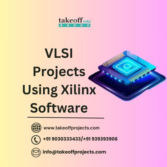
VLSI Projects Using Xilinx Software
Very Large Scale Integration VLSI Xilinx software projects entail the construction of circuits that have millions of transistors on a single chip. Xilinx offers encompassing FPGA solutions like Vivado and ISE for VLSI design where end-user can implement his/her digital system with utmost ease at high level of abstraction. Common offerings are usually of the form of ASICs that incorporate digital systems such as processors, memory interfaces, communication interfaces, or specific Circuits. One of the most selected project ideas is to develop an MIPS microprocessor on Xilinx FPGAs for ALU, control units, registers and the like. Another frequently assigned project is the synthesis of the digital signal processing (DSP) system associated with pulsing or graphic processing. Its software includes a programmable logic device programming software, FPGA development software, an integrated circuit/multi-chip module fabrication software, simulation software as well as a hardware verification and timing analysis software that helps confirms that the VLSI design is functional and efficient. These projects are useful in grasping concepts like digital logic, HDL, and the usage of FPGAs to conceptualize electronic systems.
#vlsi#xilinx#software#projects#fpgasoultion#digitalsystem#VLSIdesign#engineeringprojects#takeoffedugroup
0 notes
Text
How UVM and RVM Improve ASIC Verification Efficiency
The Key to Smooth ASIC Design, Verification, and Validation
ASIC design, verification, and validation are intricate processes that require precision and efficiency. Engineers use Universal Verification Methodology (UVM) and RVM (Reference Verification Methodology) to streamline verification, reducing risks and optimizing performance. But what makes these methodologies essential? Let’s explore how they enhance efficiency and ensure smoother development cycles.
Understanding UVM and RVM in ASIC Verification
ASIC design, verification, and validation involve multiple stages, from specification to production. Verification plays a crucial role in ensuring the design functions as intended before manufacturing begins.
UVM (Universal Verification Methodology): A standardized methodology using SystemVerilog that improves testbench reuse and modularity.
RVM (Reference Verification Methodology): A structured approach that enhances verification efficiency, particularly for legacy designs and customized workflows.
Both methodologies aim to improve test coverage, automation, and reusability, leading to faster and more reliable verification cycles.
Why UVM Matters in ASIC Verification
1. Reusability and Scalability
UVM allows engineers to create modular and reusable verification components, reducing development time. By reusing existing testbenches, verification teams save effort and ensure consistency across projects.
2. Automation and Efficiency
UVM-based testbenches integrate seamlessly with automation tools, allowing for large-scale simulations and coverage-driven verification. This automation reduces manual effort and accelerates test execution.
3. Standardization Across Projects
As an industry-standard methodology, UVM ensures that teams follow a structured approach, improving collaboration and compatibility across different ASIC design, verification, and validation projects.
The Role of RVM in ASIC Verification
1. Legacy Design Compatibility
Many verification teams work with older designs that require a structured approach. RVM provides a flexible framework for integrating legacy verification components.
2. Reference Model Integration
RVM supports the use of reference models to compare expected and actual outputs, improving error detection and debugging.
3. Customization for Complex ASICs
Unlike rigid methodologies, RVM allows customization based on project requirements, making it a viable choice for complex ASIC design, verification, and validation tasks.
Combining UVM and RVM for Maximum Efficiency
While UVM is widely adopted for new projects, RVM remains useful for legacy designs and customized workflows. Combining both methodologies can:
✅ Enhance test coverage with structured verification strategies ✅ Reduce debugging time through automated error detection ✅ Improve efficiency with modular, reusable verification environments
By strategically integrating UVM and RVM, verification teams can optimize their ASIC design, verification, and validation processes while maintaining flexibility.
Final Thoughts
ASIC design, verification, and validation demand robust methodologies to improve efficiency and accuracy. UVM and RVM provide engineers with powerful tools to optimize verification, reduce debugging time, and enhance overall chip reliability. By understanding and applying these methodologies effectively, teams can streamline development and achieve faster, more reliable results.
FAQs
1. Which methodology is better for ASIC verification, UVM or RVM?
Both have unique advantages. UVM is ideal for modern, standardized verification environments, while RVM is useful for legacy designs and reference-based verification.
2. Can UVM and RVM be used together?
Yes, combining UVM and RVM can enhance verification efficiency by leveraging the strengths of both methodologies.
3. Why is verification crucial in ASIC design?
Verification ensures that the design functions correctly before manufacturing, reducing risks and preventing costly errors in production.
0 notes