#quickturn
Explore tagged Tumblr posts
Visit Tumblr Blog
Explore Tumblr blogs with no restrictions, modern design and the best experience.
Last Seen Tumblr Blogs


Fun Fact
In Q3 of 2020, 31% of US users access the Tumblr app daily.
Text

Heavy Copper PCB Manufacturing
Over 15 years experiences of thick copper PCB
What is Heavy Copper PCB?
Heavy copper PCB is a circuit board with a copper thickness that is ≥ 3oz per sq. ft in its outer and inner layers. What makes a circuit board classified as a heavy copper PCB is its thicker plating. During the production of heavy copper PCB, copper thickness is enhanced through plated holes and sidewalls. For instance, when a PCB has 2 ounces of copper per sq. ft thickness, it is a standard PCB. However, if it has more than 3oz of copper, it is a heavy copper PCB. Heavy copper PCB is considered a reliable wiring option. Heavy copper PCB is different from extreme copper PCB which features within 20 oz to 200 oz per sq. ft.
What does Heavy Copper PCB offer?
Heavy copper PCB has a lot to offer. It has got some unique features that make it an ideal option for high-end applications. Let’s discuss some of the benefits of this PCB; Great thermal distribution: Due to its copper-plated vias, this PCB offers high thermal resistance. Heavy copper PCB are used in applications that demand high speed and high frequency. You can also use this PCB at harsh temperatures. Mechanical strength: Heavy copper PCB feature great mechanical strength. When this PCB is used, it makes the electrical system durable and robust. Good conductor: Heavy copper circuit boards are a good conductor. They are utilized in the production of electronics due to this feature. They help to link various boards together. These boards can transfer current.
How is Heavy Copper PCB Fabricated?
For the fabrication of heavy copper PCB, plating or etching is often used. The main aim is to add copper thickness to sidewalls and plated holes. The methods used in fabricating heavy copper PCB aren’t far-fetched. Heavy copper PCBs need special etching and plating methods to ensure the extra thickness of copper. Using the normal etching techniques for the fabrication of heavy copper PCBs isn’t ideal. Normal etching methods produce over-etched margins and edge lines that are uneven. PCB producers now use advanced etching and plating methods to achieve straight edges.
Heavy copper PCBs are produced via etching and plating methods. The major aim in the production of this PCB is to add copper thickness through sidewalls and plated-through holes. Heavy copper PCBs have several benefits which make them in high demand. Due to their outstanding features and benefits, they can meet your electrical requirements. These circuit boards will always dissipate heat generated due to heavy currents conduction. Electronics using heavy copper boards have been in use for a long time. Heavy copper can carry high currents. These boards will continue to meet the needs of various applications. High power circuit wirings can be developed using Heavy Copper PCBs. Such a wiring mechanism offers more reliable thermal stress handling and offers fine finishing while incorporating multiple channels on a single layer of a compact board.
Printed circuit boards (PCBs) are usually bonded with a layer of copper foil on a glass epoxy substrate. The thickness of the copper foil is usually 18μm, 35μm, 55μm, and 70μm. The most commonly used copper foil thickness is 35μm. Domestic copper foil thickness is generally 35 ~ 50μm, there are thinner than this such as 10μm, 18μm; And thicker than that like 70μm. The thickness of composite copper foil on 1~ 3mm thick substrate is about 35μm. The thickness of the composite copper foil on the substrate less than 1 mm thick is about 18μm, and the thickness of the cladding copper foil on the substrate thicker than 5mm is about 55μm. If the PCB copper foil thickness is 35μm, printed line width is 1mm, then every 10mm long, its resistance value is about 5mΩ, its inductance is about 4nH. When the di/dt of the digital integrated circuit chip on the PCB is 6mA/ns and the working current is 30mA, the noise voltage generated by each part of the circuit is estimated to be 0.15mV and 24mV according to the resistance value and inductance value of each 10mm printed line. Heavy Copper PCB boards can be made simply by combining two main processes: electroplating and etching. Compared to other PCBs, the circuit is made of a thin layer of copper foil. The copper plates are uniformly laminated with FR4 or other epoxy-based substances. The average weight of a Heavy Copper PCB can be 4 oz. (140μm), which is a better ratio than a copper-shared PCB. Let's look at the benefits.
Heavy Copper PCB Manufacturer & Circuit board Assembly – One-stop service Printed Circuit Boards (PCB) are usually coated with thick copper foil on a glass epoxy substrates commonly thickness of copper foil are 18μm, 35μm, 55μm, and 70μm. The most common copper foil is 35μm. The heavy copper PCB boards can simply be manufactured by two main processes plating and etching in the combine. As compared to other PCBs, the circuit is made of a thin layer of the Copper foil sheet. The plates of copper are laminated uniformly with FR4 or other epoxy-based substance. The average weight of the thick copper PCB weight could be 4oz (140μm), and this ratio is better as compared to another type of PCBs who have copper in common. Let’s check out the benefits of it.
Benefits of Heavy copper PCB Fabrication
Here are some of the advantages of heavy copper PCB, let’s follow them:
1. Favorable circumstances of Heavy Copper PCB
2. Plating innovation in overwhelming copper permitted a mix of plating and carving which causes in straight sidewalls and immaterial undercut.
3. The substantial copper plating creates high-current circuits and control circuits that watches the profoundly thick and straightforward whiskers’ structure.
4. This empowers the board fabricator to build the measure of copper thickness in plated gaps and by means of sidewalls.
5. The blend of substantial copper results on a solitary board called PowerLink.
6. The substantial copper in the PCB likewise encourages in associating with the standard circuits.
7. This lessens layer tally, low impedance control conveyance, littler impressions, and potential cost investment funds.
8. For development purposes, it expands the continuance to warm strains.
9. It has expanded the current conveying limit.
10. Overwhelming copper plating brings higher current through the board and moves the warmth to the outside heat sink
Application and advantage of Heavy Copper PCB in Electronic manufacturing
Heavy Copper PCB is a special PCB, its main characteristic is that the copper thickness is greater than or equal to 2oz. Compared with traditional PCB, Heavy Copper PCB has many advantages in electronic manufacturing. For example, they can withstand higher currents, have better heat dissipation capacity, better mechanical strength and better electrical properties. These characteristics make Heavy Copper PCBs widely used in high power equipment, such as electric vehicles, industrial robots, aerospace, mobile phones, microwave, satellite communications, network base station and other fields.
Take electric vehicle electronic control system as an example, electric vehicle electronic control system is one of the core components of the vehicle, has a very important role. In this kind of high-power electronic equipment, the range of current and voltage changes is very large, and the Heavy Copper PCB has better load capacity and heat dissipation capacity, which can ensure the stability and reliability of the electronic control system. Our customers use Heavy Copper PCBs in the production of electric vehicle electronic control systems to ensure the stability and reliability of the system under high power operating conditions.
When you decide to use a Heavy Copper PCB, you need to choose the right PCB manufacturer, Hitech Circuits will be able to offer copper plates in a variety of thicknesses and specifications to suit your needs. At the same time, you should ensure that your design meets the specifications and requirements of Heavy Copper PCB, including the wiring specifications of Heavy Copper PCB, welding pad specifications, etc. Finally, the right manufacturing process is also key, such as the selection of appropriate drilling, sheet laying and other processing steps to ensure quality.
In short, Heavy Copper PCB plays an irreplaceable role in the production and application of PCB industry, with high power, high current and high cooling effect. Heavy Copper PCB manufacturing process and materials have higher requirements than standard PCB. Hitech Circuits has advanced equipment and professional engineers to supply high quality Heavy Copper PCBs to domestic and international customers.
Heavy Copper circuit board technology introduction
(1) Preparation and plating treatment before plating
The main purpose of thickening copper plating is to ensure that there is enough Heavy Copper coating in the hole to ensure that the resistance value is within the range required by the process. As an insert is fixed position and ensure the connection strength; As surface-packaged devices, some holes only act as conduction holes, which conduct electricity on both sides.
Check item
a. Mainly check the metallization quality status of the hole, and ensure that there is no residue, burr, black hole, hole, etc.;
b. Check whether there is dirt or other residue on the surface of the substrate;
c. Check the number, drawing number, process document and process description of the substrate;
d. Make clear the installation and hanging position, installation and hanging requirements and the plating area that the plating tank can withstand;
e. Plating area and process parameters should be clear to ensure the stability and feasibility of plating process parameters;
f. Clean and prepare the conductive parts, and first energize the solution to make it appear active;
g. Determine whether the composition of the tank is qualified and the status of the surface area of the plate; If the cylindrical anode is used, the consumption must be checked;
h. Check the firmness of the contact parts and the fluctuation range of voltage and current.
(2) Quality control of thickened copper plating
a. Accurately calculate the plating area and refer to the effect of actual production process on current, correctly determine the required value of current, master the change of current in electroplating process, and ensure the stability of plating process parameters;
b. Before electroplating, the commissioning plate is used for test plating, so that the bath is in the activated state;
c. Determine the direction of the total current flow, and then determine the order of the hanging plate. In principle, it should be from far to near; Ensure the uniform distribution of current to any surface;
d. To ensure the uniformity of the coating and the consistency of the coating thickness in the hole, in addition to the technical measures of mixing and filtering, the impact current should be used;
e. Constantly monitor the change of current in the electroplating process to ensure the reliability and stability of current values;
f. Test whether the thickness of the copper plating layer in the hole meets the technical requirements.
(3) copper plating process
In the process of thickening copper plating, the process parameters must be monitored regularly, which often causes unnecessary losses due to subjective and objective reasons. To do a good job of thickening copper plating process, we must do the following aspects:
a. Add a certain value according to the area value calculated by the computer and the empirical constant accumulated in the actual production;
b. According to the calculated current value, in order to ensure the integrity of the coating in the hole, a certain value must be added to the original current value, namely, the impact current, and then return to the original value in a short time;
c. When the electroplating of the circuit board reaches 5 minutes, take out the substrate and observe whether the copper layer on the surface and the inner wall of the hole is complete, and the metal luster in all holes is preferable;
d. A certain distance must be kept between the substrate and the substrate;
e. When the thickened copper plating has reached the required plating time, a certain amount of current should be maintained during the removal of the substrate to ensure that no blackening or darkening will occur on the surface of the substrate or in the hole.
Note:
a. Check process documents, read process requirements and get familiar with lamina chart of substrate machining;
b. Check the surface of the substrate for scratches, indentation, copper exposure and other phenomena;
c. According to the mechanical processing floppy disk test processing, the first part of the pre-inspection, meet the technical requirements before all the workpiece processing;
d. Prepare measuring tools and other tools to be used for monitoring substrate geometry;
e. Select the appropriate milling tool (milling cutter) according to the raw material nature of the machining substrate.
Quality control
a. Strictly implement the first-part inspection system to ensure that the product size meets the design requirements;
b. Select milling processing parameters reasonably according to the raw materials of the circuit board;
c. When fixing the position of the circuit board, it should be carefully clamped to avoid damaging the solder layer and solder resistance layer on the surface of the circuit board;
d. To ensure the consistency of the overall dimension of the substrate, the position accuracy must be strictly controlled;
e. When disassembling and assembling, special attention should be paid to the layer of the substrate to pad the paper, so as to avoid damaging the plating layer on the circuit board surface.
The three characteristics of Heavy Copper PCB
1, bearing large current
When the line width is certain, increasing the copper thickness is equivalent to increasing the section area of the circuit, so the thickening of copper foil can make the circuit board carry more current.
2. Reduce thermal strain
Copper foil has a small conductivity (also known as resistivity, 1.72*10-8ΩΩ·m) through high current condition temperature rise is small, so it can reduce heat, thereby reducing thermal strain.
The conductivity is the resistivity. Metal "conductors" are divided into:
Silver → Copper → gold → aluminum → tungsten → nickel → iron.
3, Good heat dissipation
Copper foil has high thermal conductivity (thermal conductivity of 401W/mK), which can play an important role in improving heat dissipation performance, so it has good heat dissipation;
Thermal conductivity refers to the heat transferred through an area of 1m2 within 1H for a 1m thick material with a surface temperature difference of 1°C under stable heat transfer conditions. The unit is W/m·K.
Based on the above characteristics, it can be seen that Heavy Copper PCB is very suitable for high-current products. It has different characteristics and can better achieve circuit functions.
Application of Heavy Copper PCB
Heavy Copper PCBs have a number of benefits over standard PCBs. In addition, they offer excellent features that make them ideal for specific applications. For example, Heavy Copper PCBs are ideal for defense and military applications, medical devices, and many other fields. As a result, the demand for Heavy Copper PCB is increasing.
Here are some applications of Heavy Copper PCBs:
Solar energy converter
Track traction system
Nuclear power industry
Automobile industry
UPS system
Protective relay
Torque control
Safety and signal system
Welding equipment
Power line motor
Military equipment
What can Heavy Copper PCBs provide?
Heavy Copper PCBs have a lot to offer. It has some unique features that make it ideal for high-end applications. Let's discuss some of the benefits of this PCB;
• Great heat distribution: This PCB provides high thermal resistance due to its copper-plated through-hole. Heavy Copper PCBs are used in applications requiring high speed and high frequency. You can also use this PCB in harsh temperatures.
• Mechanical strength: Heavy Copper PCBs have very high mechanical strength. When used, this PCB makes the electrical system durable and rugged.
• Good conductor: Heavy Copper circuit boards are good conductors. Because of this property, they are used in the production of electronic products. They help hold the various plates together. These plates can transmit electricity.
• Onboard radiators: Heavy Copper PCB provide onboard radiators. Using these plates, you can achieve an effective radiator on a Mosaic surface.
• Large dissipation coefficient: Heavy Copper PCBs are ideal for large components with high power consumption. These PCBs prevent the electrical system from overheating. They dissipate heat effectively.
Hitech Circuits is a professional PCB manufacturer with extensive experience in manufacturing Heavy Copper PCBs, as well as your other product requirements. We support sample and mass production, welcome to your inquiry.
0 notes
Text
Looking for reliable Quickturn PCB services in Syracuse? Get high-quality, fast-turnaround printed circuit boards tailored to meet your needs. Whether for prototyping or production, we ensure precision and efficiency. Contact us today for top-notch PCB solutions delivered on time!
0 notes
Text
Quickturn PCB Assembly: How to Build and Mount Your First Circuit Card Efficiently
In today’s fast-paced electronics market, turning a prototype idea into a working product quickly can mean the difference between leading innovation or falling behind. That’s where quickturn PCB assembly plays a vital role allowing developers to create and test functional circuit card assy units in record time. If you're new to this process, understanding how to efficiently build and mount your first circuit card is key to a successful hardware project.
circuit card assy
0 notes
Text
Vague Timeline
Pre-War: youngling Quickturn went along to many of the early rallies held by what would become the Decepticon movement. At one such event, Enforcers deliberately antagonized attendees into rioting, and used the chaos as an excuse to brutally arrest as many as possible, including one of Quickturn's creators. She never saw him again.
Early War: slim and nimble, despite her age Quickturn proved a good scouting asset, darting too swiftly for enemy anti-aircraft measures to hit. She moved between units, always on the frontline, meeting many fellow Cons and maintaining a few strong friendships with those she managed to see frequently.
Settled Factions: with the absorption of the remaining Senate forces into the Autobots under Optimus Prime's command, scouting turned into hunting. Being able to track down and take out key individuals could turn the tide of a battle just as much as dropping a dozen tanks onto the field; Quickturn specialized in spotting and removing sniper nests, as well as killing the odd tactical officer who strayed too far from their command headquarters.
The Long Hard Slog: Autobot anti-aircraft and tactical measures improved. Quickturn began joining more and more proper skirmishes, looking for the battlefield commanders to target. She started seeing more of the Decepticon ground forces; began to get a clearer picture of her faction. On one occasion, she received orders to capture rather than kill a particular target, and via some garbled orders, wound up escorting the prisoner all the way to Darkmount's dungeons. The screams left her... unsettled.
End Days: as a matter of personal honor, Quickturn began to linger upon battlefields after the fighting finished, seeking out and executing any Autobots who remained. This earned her a gruesome reputation as someone hungry for more kills, who High Command didn't bother to send after mecha they wanted alive; in truth, she preferred to see the Bots die swift, rather than be dragged away to unknown fates - interrogation, torture, experimentation, all of it made her tank churn. Quickturn kept her kills as fast and painless as possible.
Tyger Pax: eventually, though, someone in Command did tap Quickturn for another capture mission, an extremely important one. The Autobots sought to send the Allspark itself off world, and that could not be allowed to happen. So she set personal honor aside, and participated in chasing down and corning a fast yellow scout, who refused to say a word even as he was pinned and bound and taken directly to Megatron. Quickturn witnessed the questioning from a distance; she also saw her frustrated Lord rip out the scout's voicebox, and drop him from the mountainside
Final Flight: from then on, Quickturn refused to capture any Autobots alive. Her squadron leader didn't demand it, preferring to simply turn her loose on a fight and make note of the kill count later. And that would have been that, if one more order didn't come down, to seize a particular bot - and order which Quickturn ignored, in favor of killing the femme in question the first chance she got. The official reprimand only made her scoff, and insist she'd never take an Autobot alive again. The very next battle, two other members of her squadron flying guard positions overhead took aim, and shot Quickturn down.
Darkness: the crash took her down deep into Cybertron's underlayers, where manufactured metal gave way to natural stone, and creatures either slept out the drought or hunted for their meals. Damaged badly, Quickturn could not move easily, couldn't fly, couldn't see - her optics shattered upon impact, armor mostly torn away, wings crumpled and one arm completely slagged. Survival became top priority. Survival became... the only priority. Corrosion took hold in a section of her exposed processor, making it difficult for her to think clearly. Baseline, instinctive coding took charge. All through the Autobot and Decepticon evacuations of Cybertron, through the battles that began taking place on far distant worlds, a single Seeker remained trapped underground, and began to forget herself in the struggle to remain alive.
And Then, Light: a few years following the War's official end, an Autobot stumbled down into her tunnels by accident. He offered energon; she pointed him in the direction of a way out; he kept coming back. A small organic creature came along too, and started fixing her, one piece at a time. Bumblebee and Raf. And when she couldn't recall her own designation, they offered her one: reference to an organic creature with similar wings as her own. Dragonfly.
Now: sight and sanity restored, Dragonfly is making a new life for herself. Cybertron is slowly rebuilding; more and more humans are making overtures of friendship and trade. Life beyond war isn't something Fly ever imagined for herself; she's looking forward to figuring it out.
0 notes
Video
youtube
Mazak Machine - Quick Turn 250MSY
#mazakindia #samautomation #quickturn #millingmachine #turbine #coupling #machinecomponents #mazakmachine #mazak #cncmachine #spareparts
0 notes
Text
yeah, as someone who went in 100% expecting the tank controls to suck I actually love the classic RE trilogy and the tank controls are actually pretty well balanced for the gameplay, I never felt like I was at a severe disadvantage because of them. although I will admit having quickturn (which idk if that was always a part of the games or added in the pc patches of the games) helped a lot
the original resident evil trilogy is so good. when will the masses turn to the light (understanding that tank controls have a pretty gentle learning curve if you go in willing to develop familiarity with something new and that the slower pace of play they engender is a valid design choice rather than some sort of zany relic of a more primitive age of game design)
17 notes
·
View notes
Video
instagram
Custom canvas patches🤘Quick turn around ⚡️Bands, MMA, clothing brands and retail. No minimums 🔥 #custommade #custompatch #patch #denimpatch #bands #mmafighter #mmaschool #retail #shopsmallbusiness #quickturnaround #quickturn #canvaspatch #punkpatch #punkpatchesforsale #design #designer #graphicdesigner #graphicdesign https://www.instagram.com/p/CQfTECrpoH8/?utm_medium=tumblr
#custommade#custompatch#patch#denimpatch#bands#mmafighter#mmaschool#retail#shopsmallbusiness#quickturnaround#quickturn#canvaspatch#punkpatch#punkpatchesforsale#design#designer#graphicdesigner#graphicdesign
0 notes
Photo

The most #awkward sign in #newjersey #sign #road #whodrives2/10ofamile #driving #traffic #roaddog #295 #highway #triplife #outandabout #unique #onlyinnj #njmakestheworldtakes #quickturn #nosense #icantdrive55 #speedlimit #ytho (at Fieldsboro, New Jersey)
#speedlimit#traffic#295#njmakestheworldtakes#whodrives2#outandabout#onlyinnj#nosense#icantdrive55#sign#ytho#driving#newjersey#road#highway#roaddog#awkward#triplife#unique#quickturn
1 note
·
View note
Text
hhhhhh my mom had the gall to bring it up that i’m the first generation in my family to not get equal or more education than the prior gen... i need 2 go back for a masters like.... now
#personal#i've been in apparel for 4.5 months now and i wanna stay at my company bc well... HUGE brand and also.. i like them LOL#after month 3 i started getting like... weekly recruiter emails on linkedin now too???? wtf i'm not leaving this industry LOL#and like...... literally every person following me has definitely seen kids wearing crap i've worked on LOLOLOL#like cuz it's global too#and i work in quickturn event graphics.... which.. i won't give more deets than that#it's incredible childrens apparel was my second choice w/ my digital design degree....#and the SECOND i started looking for apparel graphic design positions i got offers........... fuck animation contract work#one of my besties is literally on medicaid while working on a major broadcast show wtaf#grazugruerhniefnie being interviewed for an UNpaid internship for a disney show....... illegal af#or minimum wage for fucking.... marvel... FUCK????? what the fuck????#me now: has salary... good benefits... PTO????? fuck animation it preys on passion
2 notes
·
View notes
Photo

Quick turn in and out. #aviation #aviationphotography #avgeek #rotorcraft #helicopter #astar #as350 #airbus #airbushelicopters #klbb #citationlatitude #cessna #aviationlineservicetechnician #quickturn #canonphotography #lightrooom (at Lubbock Preston Smith International Airport - LBB) https://www.instagram.com/p/Bw7wUBdgc7O5TQhreTgvI_ZWXzqPBLAz3aRth80/?utm_source=ig_tumblr_share&igshid=f493xnhooxk6
#aviation#aviationphotography#avgeek#rotorcraft#helicopter#astar#as350#airbus#airbushelicopters#klbb#citationlatitude#cessna#aviationlineservicetechnician#quickturn#canonphotography#lightrooom
0 notes
Link
Pioneer Cuts is your one-stop shop for all your CNC turning services. Our team is highly experienced with manufacturing technology and we never compromise with quality. For more requests a free quote today.
#Aerospace Prototyping Michigan#CNC Shops#Quickturn Machining#CNC Service#CNC Turning#CNC Rapid Prototyping#CNC Machining Prototype#Quick Turn CNC Machining#CNC Machining Prototype Service#Precision CNC Machine Shop
1 note
·
View note
Text
Accelerate your electronics projects in Syracuse with Quickturn PCB services. Our rapid turnaround ensures precision and reliability, empowering you to meet tight deadlines and deliver high-quality products to market faster than ever before.
0 notes
Text
quickturn
Quickturn refers to the fast manufacturing and delivery of printed circuit boards (PCBs), ideal for rapid prototyping and time-sensitive projects. Quickturn PCB services accelerate development by providing boards in as little as 24 hours. Engineers rely on quickturn manufacturing for testing ideas, verifying designs, or launching new products swiftly. This service is crucial for startups and R&D teams looking to reduce time-to-market and stay competitive.
quickturn
0 notes
Text
Uppercut turns, trying to find the mech who called her name; she's still jittery with how new the truce is and the noticeable absence of both Megatron and Optimus. She visibly relaxes and brightens when she sees who it is.
"Quickturn!" Uppercut sets the box aside and jogs to close the gap between them. "You're here -- you made it! When you didn't show up on the Nemesis, I thought... But you're really here!" Her servos flutter about, ghosting inches above Quickturn's plating, unsure if she'll accept physical touch or not. "You look good."
@meditank started following you
That... is a face she knows.
It takes a moment of staring, of watching the other pick up a crate marked for the medical building before the memory clicks home in Dragonfly's processor.
Whether the other (former?) Decepticon will recognize her in turn is, less certain.
Still. Dragonfly strides across the small courtyard, at an angle to the medic, and quietly calls "Uppercut," before getting too close.
3 notes
·
View notes
Photo
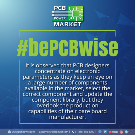
#bePCBWISE
It is observed that PCB designers concentrate on electronic parameters as they keep an eye on a large number of components available in the market, select the correct component and update the component library, but they overlook the production capabilities of their bare board manufacturer.
1 note
·
View note