#smtassembly
Explore tagged Tumblr posts
Visit Tumblr Blog
Explore Tumblr blogs with no restrictions, modern design and the best experience.
Last Seen Tumblr Blogs


Fun Fact
Tumblr is used by 21% of adults online aged 18-29 years.
Text
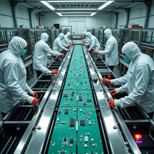
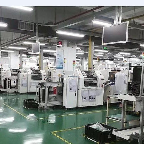
A team of skilled technicians working in a controlled cleanroom environment, assembling high-precision PCBs on an automated production line. This image represents the future of electronics manufacturing—scalable, reliable, and quality-driven. Discover end-to-end PCB design and manufacturing services at www.auckam.com.
#PCBManufacturing#ElectronicsAssembly#MadeInIndia#PCBDesign#ContractManufacturing#CleanroomTechnology#SMTAssembly#ElectronicsEngineering#IndustrialAutomation#AuckamTechnologies#HardwareDevelopment#IoTSolutions#MedTechElectronics#EmbeddedSystems#PCBIndia
0 notes
Text
Revolutionizing Electronics Manufacturing with Robotic Soldering Station in India
The electronics manufacturing industry is witnessing a rapid transformation, with automation becoming a key factor in enhancing productivity, precision, and consistency. One of the most groundbreaking innovations driving this change is the Robotic Soldering Station in India. Designed for high-speed and high-precision soldering tasks, these stations are quickly becoming indispensable in modern production lines.
A Robotic Soldering Station in India offers unparalleled accuracy in soldering small electronic components, making it especially valuable for industries like automotive electronics, telecom, consumer devices, and medical equipment manufacturing. These systems are engineered to perform repetitive soldering tasks with minimal variation and human error, ensuring uniform quality across thousands of units.
The key advantage of robotic soldering stations lies in their automation capabilities. With programmable logic controllers (PLCs) and motion control systems, these machines follow exact soldering patterns and temperature profiles. This results in stronger, cleaner solder joints and drastically reduces the risk of issues like cold soldering or component overheating. For manufacturers aiming to meet international quality standards such as IPC-A-610 or ISO 9001, robotic soldering is a game-changer.
Indian industries are quickly recognizing the long-term benefits of adopting automation, and the demand for robotic soldering systems is on the rise. Companies like Ascomp Inc. are at the forefront of supplying cutting-edge Robotic Soldering Station in India that match global performance benchmarks while remaining cost-effective. Their solutions come equipped with intelligent features like temperature sensors, real-time monitoring, and easy programming interfaces, making them ideal for both high-volume production and R&D labs.
Moreover, robotic soldering stations contribute significantly to workplace safety and efficiency. By minimizing human involvement in high-heat operations, these machines reduce the chances of workplace accidents and exposure to harmful soldering fumes. Paired with fume extractors, they create a safer and healthier work environment for technicians.
Another compelling benefit of investing in robotic soldering is the consistency and scalability it offers. Whether you're working with through-hole or surface mount components, a robotic station ensures repeatable quality—something that’s nearly impossible to achieve manually on a large scale. This consistency directly translates to fewer product returns, higher customer satisfaction, and improved brand reputation.
As India continues to strengthen its position as a global electronics manufacturing hub, the role of robotic systems will only become more significant. Businesses that invest early in automation not only gain a competitive edge but also future-proof their production processes against rising labor costs and global quality demands.
#RoboticSoldering#AutomationIndia#SolderingTechnology#AscompInc#ElectronicsManufacturing#MakeInIndia#SMTAssembly#SmartFactoryIndia#SolderingSolutions#IndustrialAutomation
0 notes
Text

Hitech Circuits—Your Reliable Supplier for Premium PCB Assembly
At Hitech Circuits, we specialize in high-efficiency, high-precision surface mount technology (SMT) assembly, delivering unmatched capacity and quality for your PCB projects.
Our Capabilities:
1. Massive Daily Output
1 Million+ Components Placed Daily**: Powered by fully automated SMT lines (e.g., Fuji NXT, Siemens SIPLACE) and high-speed pick-and-place systems, we ensure rapid production scaling for both prototypes and bulk orders.
2. Advanced Packaging Expertise
QFN/BGA Mastery: Our precision equipment handles ultra-fine-pitch components, including QFN (0.3mm pitch) and BGA (down to 0.2mm ball diameter), with 99.99% placement accuracy.
X-Ray Inspection: 100% in-line X-ray verification for BGA solder joints, voids, and alignment defects, ensuring zero hidden faults.
3. End-to-End Quality Control
AOI + SPI Integration: Automated Optical Inspection (AOI) and Solder Paste Inspection (SPI) at every stage.
IPC-A-610/612 Compliance: Certified processes for mission-critical applications.
Why Choose Us?
Speed-to-Market: 48-hour prototype turnaround & 10-day mass production cycles.
Flexible MOQs: Support for small-batch R&D to 100k+ volume orders.
Global Material Sourcing: Access to a vetted network of component suppliers, reducing lead times.
Contact Us Today!
Let’s optimize your PCB assembly with speed, precision, and reliability.
Email:[email protected]
Tel & Whatsapp: +86-180333061378
Location: Building C, Suojia Technology Park, Hangcheng, Xixiang, Shenzhen, Guangdong, China
Authority certification: we're fully ISO9001:2015, ISO14001:2015 , UL (E354070) and RoHS certificated. You can reply on us for custom PCB production and Electronic assembly.
1 note
·
View note
Text
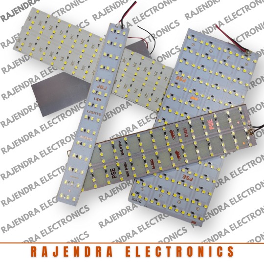
SMD PLATE AVAILABLE IN ALL RUNNING SIZES ( 42 , 84 , 126 & 168 )
STOCK AVAILABLE !!!
For any Query:
☎ : +91-9899391155, +91-9910772484
Know More: https://www.indiamart.com/rajendra-electronics-newdelhi/
Facebook: https://www.facebook.com/profile.php?id=61550818087962
Instagram: https://www.instagram.com/rajendra.electronic/
LinkedIn: https://www.linkedin.com/in/rajendra-electronics-144b73290/
Reddit: https://www.reddit.com/user/Rajendra_Electronics
Youtube: https://www.youtube.com/@Rajendra_Electronics/about
Twitter: https://twitter.com/Rajendra_Elec
Pinterest: https://in.pinterest.com/rajendraelectronics314/
Tumblr: https://www.tumblr.com/blog/rajendra314
#smdplate #surfacemountdevice #pcbassembly #electronicsengineering #soldering #smtcomponents #ElectronicsDesign #PCBproduction #smdtechnology #solderingstation #circuitboard #electroniccomponents #techinnovation #smtassembly #electronicsmanufacturing #solderingtools #electronicprojects #smdassembly #smtsoldering #techprototyping
0 notes
Text
1 note
·
View note
Photo
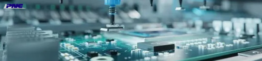
Bill Of Materials Management In PCB Design Process
Managing the Bill of Materials in the PCB design process can be a complex and time-consuming endeavor. Luckily, there are ways to make this process easier and more efficient. So, we will explore how to streamline BOM management in design so that you can save time and money. You will learn the best practices for maintaining an accurate BOM, methods for keeping track of changes, and tips for improving the overall design process. With these strategies, you can produce high-quality products faster and more effectively.
For more details visit: Read more: https://bit.ly/3NvIz9X Website: https://pnconline.com Twitter: https://twitter.com/PNCINC Facebook: https://www.facebook.com/PNCONLINE Pinterest: https://www.pinterest.com.au/rrosh2014/ Bresdel: https://bresdel.com/pncinc Myspace: https://myspace.com/pncinc2020 Address: 115 East Centre St. Nutley, NJ, 07110 Call us: (973) 284-1600 Email us: [email protected]
#pcbboardassembly#pcbassembly#smtassembly#printedcircuitboardassembly#printedcircuitboardassemblycompanies#smtassemblyservice
0 notes
Photo

EITPL provides the best of the practices for #pcba /printed circuit board assembly /box build assembly with Cost-effective manufacturing and highly proficient PCB Testings.To know more visit - https://eitplems.com/Or Call us
0 notes
Photo

When you are looking for substrates for electronic circuits with a high thermal conductivity and a low expansion coefficient, ceramic PCB will be your preferred choice of material. #kinglisheng is a very good provider of that! http://eng.jlspcba.com/
0 notes
Photo

#pcba #assembly #modules #manufacturer #makers #industrial #thtassembly #populated #factory #china #smtassembly #electronics #circuitboard #module #engineering #electronics #embedded #embeddedsystems #machine https://www.instagram.com/p/BnCnjA6AxbN/?utm_source=ig_tumblr_share&igshid=1muyxbyp6zgq8
#pcba#assembly#modules#manufacturer#makers#industrial#thtassembly#populated#factory#china#smtassembly#electronics#circuitboard#module#engineering#embedded#embeddedsystems#machine
0 notes
Text
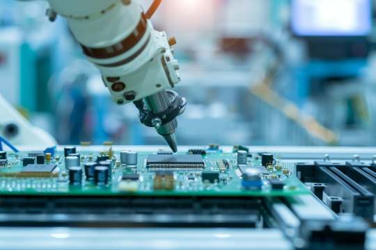
A high-precision robotic arm performing automated soldering on a printed circuit board (PCB) in a clean electronics manufacturing environment. Ideal for showcasing SMT assembly, embedded systems, smart devices, and high-reliability electronics production. Powered by advanced automation and Industry 4.0 technologies. Visit www.auckam.com for expert electronic manufacturing solutions.
#PCBA#ElectronicsManufacturing#SMTAssembly#AutomatedSoldering#EmbeddedSystems#SmartElectronics#Industry40#IoTDevices#PCBDesign#ElectronicsEngineering#Auckam#EMSPartner#CleanroomTech#ElectronicProductDevelopment#ManufacturingInnovation
0 notes
Text
Analysis Of Solder Beads Defects In SMT Assembly
SMTAssembly Solder Beads Defect Explanation
SMT Assembly solder beads defects not only affect the appearance but also cause bridging defects. Simply speaking, solder beads can be divided into two categories: One type appears on one side of the SMD component, often in the shape of an independent large ball (see Figure 1 below); The other type appears around the IC pins and which is in the shape of scattered beads.

Picture: Solder beads are located on the waist side of the component


Analysis of the Causes of Solder Beads Defect in SMT Assembly
Factor A: The temperature curve is incorrect▼
The reflow curve can be divided into 4 sections: Preheating, heat preservation, reflow and cooling. The purpose of preheating and heat preservation is to increase the surface temperature of the PCB to 150°C within 60-90s and keep it warm for about 90s so that it not only reduces the thermal shock of PCB and components, but also ensures that the solvent of the solder paste can be partially volatilized. Avoid splashing caused by too much solvent during reflow soldering, causing the solder paste to rush out of the pad and form tin beads.
Solution
The factory should pay attention to the heating rate and adopt moderate preheating to make the solvent fully volatilize

Factor B:The quality of solder paste▼
①The metal content in the solder paste is usually (90±0.5)℅. Too low metal content will cause too much flux composition, and too much flux will cause flying beads due to the fact that it is not easy to volatilize during the preheating stage;
②The increase of water vapor and oxygen content in the solder paste will also cause flying beads. Since solder paste is usually refrigerated, when it is taken out of the refrigerator, if it is not fully warmed to thaw and stirred evenly, water vapor will enter; in addition, the lid of the solder paste bottle must be tightly closed after using every single time. If it is not tightly closed in time, which will definitely cause the entry of water vapor;
③After the solder paste printed on the stencil is completed, the remaining part should be treated separately. If it is put back in the original bottle, the solder paste in the bottle will deteriorate and tin beads will also be produced;
Solution
The factory is required to choose high-quality solder paste and pay attention to the storage and use requirements of the solder paste.

Other factors include ▼
①The printing is too thick, and the excess solder paste overflows after the component pressed down;
②The pressure of the patch is too high, and the downward pressure will cause the solder paste to collapse onto the solder mask;
③The shape of the pad opening is not good, and no anti-tin bead treatment has been done;
④The activity of the solder paste is not good, it dries too fast, or there are too many small tin powders;
⑤The printing is offset, so that part of the solder paste is stained on the PCB;
⑥The scraper speed is too fast, causing bad edge collapse, and solder balls after reflow.
http://www.58pcba.com/index.php?id=1085
#smt assembly#solder beads#pcba manufacturing#EMS Manufacturer#Grande#printed circuit board assembly#electronics manufacturing services
0 notes
Link
Our PCB assembly services include SMT assembly, mixed technology, and through-hole in a ESD protected, humidity controlled environment. Our high speed SMT lines are equipped with solder paste inspection, 40” high definition Inspection monitors with max magnification at 600X, 13 zone re-flow ovens and 3D AOI. Through-hole capabilities include an 18’ slide line with four high definition monitors, wave solder, or the use of the latest selective soldering technology equipment. PNC’s final inspection area includes (4) inspection stations with high definition monitors designed for employee ergonomic comfort.
Quantities range from small-number prototypes to large production orders. We serve the military/defense, medical, aerospace, automotive, industrial and consumer sectors. Since we have the capability to design and fabricate printed circuit boards in the same facility, we are able to turn concepts into prototypes in as little as 24 hours. Other PCB assembly services include functional testing, programming, conformal coating, 3D X-Ray, box builds, lead free and leaded rework stations.
The PNC Inc. quality system ensures that our employees are IPC-A-610 and IPC-J-STD Class III-qualified. Company certifications include, AS9100D, ISO 9001-2015, MIL-PRF-55110 and MIL-PRF-31032. Our SMT assembly area are ITAR-restricted per mil standards. We are ESD compliant to ANSI/ESD S20.20.
PRINTED CIRCUIT BOARD ASSEMBLY CAPABILITIES

Surface Mount Technology (SMT)
We utilize state of the art Universal and Juki Pick & Place equipment in our SMT assembly division. These machines are capable of placing 17,100CPH to 23,500CPH with capacity to accommodate 160 8mm Electronic tape feeder with placement accuracy of +/-.05mm. Our Heller 13 zone re-flow ovens have 26 Independent temperature-controlled heating zones to accommodate the right profile whether the printed circuit board assembly is for double sided or multi-layer PCB’s.
Components as small as 0201 package size
Package types: QFPs, uBGAs, QFN, and BGAs
Two-sided assembly for Rigid, Flex and Rigi-Flex PCBs
Ability to do IPC-A-610 Class 1, 2 and 3
RoHS and Leaded assembly
THRU HOLE TECHNOLOGY
PCB assembly services in the through-hole arena are many. Our expertise with Axial, Radial, DIP, Right Angle connectors, Header connectors, SIP sockets and pogo pins, to name a few that we work with daily. A majority of these components are soldered with the latest selective solder machine that is nitrogen assisted for hole fill consistency per IPC class standards. If the PCB assembly is 100% through-hole, we utilize an 18’ slide line equipped with 4 inline workstation high definition monitors to display each operators work tasks. This type of printed circuit board assembly would be passed through our wave soldering machine for mass production soldering.
Highly Skilled Staff IPC J-Std-001 trained and certified
Manual Through Hole Assembly
Custom Slide line for larger volume
Press fit connectors
Wave soldering
Select solder machine for Lead and Lead-free (RoHS) products
MIXED TECHNOLOGY
Most PCB assembly will require some type of through hole devices. Since this type of printed circuit board assembly has SMT components previously installed, the through-hole devices will be selectively soldered. Our ERSA selective soldering machine is nitrogen assisted to achieve the highest quality solder joints to meet IPC hole requirements.
PCBA CLEANING
Paste used in our SMT assembly lines is a no clean paste, but we clean 100% the PCBA’s providing there are no components on the printed circuit board assembly that cannot be aqueously cleaned, such as displays, switches, etc. Our Nano Jet Inline cleaning system is capable of both water and aqueous chemical cleaning applications based on customer requirements.
BOX BUILD ASSEMBLY
PNC not only offers full turnkey PCB assembly, but also integrating the printed circuit board assembly into enclosures. Our experience in box builds come in many different sizes, shapes and enclosure materials. Our capability of enclosure assemblies is from snap together plastic housing to metal form factors that require torque specifications.
Plastic/Metal enclosures
Mechanical assemblies
Kitting, labelling and packaging of finished product with all components and documentation
Direct ship to distributors or end customers
0 notes
Photo

EITPL team of professionals ensures you get the best-in-class Surface Mount PCB Assembly in all sizes and for all electronic devices. Call us @+919650274009
0 notes
Photo
PCB assembly line #PCBAfactory #PCBAshop #pcbassembly #pcba#workshop #chinafactory #pcba #assembly #smtassembly #thtassembly #fuji #fastrun #factory #OEM #EMS #R&D #ODM #engineering #assemblyline #pcbturnkey #manufacturing #production #turnkey #fabrication #design #research #shenzhen #juki #CME #cable #manufacturer #lowcost #parts #components #populated #soldering #electronics #circuits #boards #pcb
#factory#assemblyline#fastrun#pcbashop#juki#assembly#turnkey#manufacturer#smtassembly#r#cable#design#shenzhen#odm#electronics#pcbassembly#components#ems#production#pcba#manufacturing#engineering#parts#boards#fabrication#research#lowcost#populated#fuji#soldering
0 notes
Text
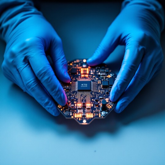
A close-up view of a precision-engineered PCB (Printed Circuit Board) held by gloved hands in a cleanroom environment. The board showcases advanced embedded electronics used in smart devices, drones, and industrial applications. Ideal for high-reliability and low-noise design requirements.
Use this image for articles or pages focused on custom PCB layout, embedded system design, electronics manufacturing services, or drone controller board engineering. Explore more at Auckam Technologies – your trusted partner in high-performance electronics and embedded product development.
#PCBDesign#ElectronicsManufacturing#EmbeddedSystems#DroneElectronics#PCBA#SMTAssembly#IoTDevices#CircuitBoardDesign#ProductEngineering#HardwareDesign
0 notes
Text
Electronic Manufacturing in Chennai — A Complete Industry Overview

If you’re exploring electronic manufacturing in Chennai, you’re looking at one of India’s fastest-growing and most dynamic industrial sectors. Chennai has emerged as a key hub for EMS (Electronics Manufacturing Services) and PCB design, attracting both domestic and international companies seeking quality, efficiency, and innovation.
This comprehensive overview will help you understand why Chennai is a preferred destination for electronics manufacturing, what the local industry offers, and how it can support your product development needs.
Why Chennai is a Leading Electronics Manufacturing Hub
Chennai’s rise as an electronics manufacturing center is driven by several unique advantages:
Strategic Location and Connectivity
Chennai offers excellent access to major ports like Chennai Port and Ennore Port, facilitating smooth import and export of components and finished goods. The city is well-connected via road, rail, and air to key markets across India and globally.
Skilled Workforce and Technical Expertise
Chennai is home to numerous engineering colleges and technical institutes that supply a steady stream of qualified engineers and technicians. This talent pool is well-versed in modern PCB design and electronics manufacturing processes, supporting innovation and quality.
Robust Infrastructure and Industrial Clusters
Dedicated electronics manufacturing zones, such as Sriperumbudur and Oragadam, host advanced industrial parks with reliable power, logistics, and facilities tailored for electronics production.
Government Support and Incentives
Tamil Nadu’s electronics manufacturing policy encourages investments through subsidies, incentives, and streamlined approvals. National initiatives like Production Linked Incentive (PLI) schemes further boost the sector.
Key Components of Electronic Manufacturing in Chennai
Electronics Manufacturing Services (EMS)
EMS companies in Chennai offer end-to-end manufacturing solutions, including:
Prototype development and New Product Introduction (NPI)
Printed Circuit Board Assembly (PCBA) with Surface Mount Technology (SMT) and Through-Hole Technology (THT)
Box build assembly and product integration
Testing, quality control, and compliance assurance
These companies serve diverse sectors such as consumer electronics, automotive, healthcare, industrial automation, and IoT devices.
PCB Design and Manufacturing
Advanced pcb design capabilities are a cornerstone of Chennai’s electronics ecosystem. Local companies specialize in multilayer PCB layout, high-density interconnects (HDI), and design for manufacturability (DFM), enabling efficient production and performance optimization.
PCB manufacturing units support these designs with precise fabrication, assembly, and inspection processes.
Trends Shaping the Electronics Manufacturing Industry in Chennai
IoT and Smart Devices: Increasing demand for connected devices is driving innovation in EMS and PCB design services.
Automation and Industry 4.0: Adoption of robotics and AI-powered quality control is enhancing manufacturing precision.
Sustainability: Growing focus on eco-friendly materials and energy-efficient manufacturing practices.
Export Growth: Chennai’s electronics exports are rising steadily, supported by favorable trade policies and global demand.
How to Choose the Right EMS Partner in Chennai
When selecting an EMS company in Chennai, consider the following factors:
Technical expertise in PCB design and advanced manufacturing technologies
Quality certifications such as ISO and IPC standards compliance
Manufacturing capacity and scalability to support your product lifecycle
Transparent communication and project management for smooth collaboration
Conclusion
Electronic manufacturing in Chennai is a thriving, well-supported industry with strong infrastructure, skilled talent, and innovative EMS providers. Whether you are a startup or an established company, Chennai offers a reliable ecosystem to develop, manufacture, and scale your electronic products efficiently.
Understanding the local capabilities in pcb design and EMS will help you make the best choices and accelerate your product’s journey from concept to market success.
#ElectronicManufacturing#EMSIndia#PCBDesignChennai#ElectronicsInChennai#PCBAIndia#SMTAssembly#ElectronicsManufacturingServices#PCBManufacturingIndia#ChennaiEMS#ManufacturingInChennai
0 notes