
Don't wanna be here? Send us removal request.
Statistics
We looked inside some of the posts by pcbdesignworld-blog and here's what we found interesting.
Average Info
Notes Per Post
4
Likes Per Post
3
Reblog Per Post
0
Reply Per Post
1
Time Between Posts
5 days
Number of Posts By Type
Text
10
Photo
1
Last Seen Tumblr Blogs


Fun Fact
Women make up for the other 50% of Tumblr’s audience.
Text
SMT Soldering Process in PCB Assembly Factory

Generally, a good PCB manufacturer provides various services like SMT Assembly, BGA Assembly, Through-Hole Assembly, Mixed Assembly, Rigid-Flex PCB Assembly Services, etc. and they are in compliance with a wide range of standard including IPC 610 Class 2 and Class 3. PCBs are found in almost every Electronic device and with the increased demand for Electronic devices all around the world, their production rate is increasing day by day. There are many small and big PCB manufacturers all over the world and all are trying to provide quality services and customer satisfaction to stand out in the competition. Though their services can differ in terms of quality and number but they follow almost the same PCB assembling process to build the PCB. So today we will discuss the PCB assembly process in detail. https://pcbdesignworld.com/article/smt-soldering-process-in-pcb-assembly-factory
2 notes
·
View notes
Text
PCB Design Guidelines for Assembly (DFA)

Assembly in PCBs involves combining the board with other components, such as the connectors, heat sinks, enclosures, etc, to make up the full product. PCB assembly should be put into consideration early enough during the design process so that we do not end up with a PCB that does not fit right into our product.
https://pcbdesignworld.com/article/pcb-design-guidelines-for-assembly
1 note
·
View note
Text
PCB Track Width and Track Resistance – Importance, Calculation, and Design Tips

PCB boards are the basic element of all the electronic devices that we are using today. These PCB boards are used to minimize the size and complications that are involved in the wired circuits. The wires in typical circuits are converted as tracks in a PCB. Just like a wire, these tracks also have their own resistance and the maximum current that flow through it depends on its width. Further the width and resistance of the track also decides the voltage drop across the track. So, it is very important for a PCB Designer to calculate the right width and Resistance of his tracks
0 notes
Text
PCB Grounding Techniques that Every Designer Should Know

A proper Grounding is important for any circuit to work as designed, the importance of grounding cannot be stressed enough especially if the circuit consists of many analog and switching components. When designing a Printed Circuit board (PCB) the designer should ensure that all the ground signals are free from noise. There are many grounding methodologies in PCB design that are followed by engineers, the common ones are like including a common ground point, ensuring an efficient flow of signals to ground, reducing the use of series vias, etc.. These techniques help us to keep the PCB ground free from the noise. In this article, we will look into all these common ground practices to design PCBs that are free from ground noise.
0 notes
Text
PCB Quality Control – Things to validate during Design, Fabrication, Procurement, and Inspection

Any flaw in a PCB quality will not only make the board unfit to use but will also waste the complete time and money spent in assembling and processing the board through the manufacturing line. This is why PCB Quality Check is performed on each board and the faulty board is removed before it reaches the assembly line.
https://pcbdesignworld.com/article/pcb-quality-control-and-things-to-validate-during-design-fabrication-procurement-and-inspection?fbclid=IwAR3hx515C-NJEJi2Sd9yPKqtd_EGIAo-lgGXpaJaJOYNN4ENIhz5BnYCBCE
0 notes
Text
Creating Custom Parts and Schematics in KiCad PCB Software


One common task, designers deal with when designing schematics is the need to create a new symbol.
In this article, we will focus on creating custom parts, connecting components neatly using the bus tool, Assigning Footprints to symbols and Generating Netlists in kicad.
Check out complete tutorial https://pcbdesignworld.com/article/kicad-tutorial-3/5-creating-custom-parts-and-schematics
0 notes
Text
Drawing Schematics on KiCad

Develop the schematic diagram for your printed circuit board using KiCad. We will start by creating a KiCad project and work with the EEschema interface, along with placing components and connecting them according to your circuit design.
In this process of learning, we will also build an example project, which will be creating a 7-segment display driver circuit using the CD4511 BCD to 7-segment driver IC
Check out the complete tutorial https://pcbdesignworld.com/article/kicad-tutorial-2/5%E2%80%93drawing-schematics-on-kicad
0 notes
Text
Getting Started with KiCad
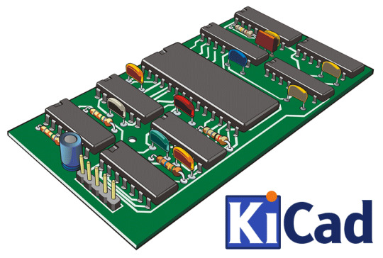
KiCad is an open-source software suite containing a series of software used in computer-aided electronics design.
In this tutorial, we will explore the origin of KiCad, why it was selected above the others, advantages, disadvantages and finally installing and getting around its interface.
Check out complete tutorial https://pcbdesignworld.com/article/getting-started-with-kicad
0 notes
Text
Understanding the IPC standards for PCB design.

IPC is a trade association that sets the standards and benchmarks for assembling and protecting the electronic equipment.
Read full article https://pcbdesignworld.com/article/understanding-the-ipc-standards-for-pcb-design
0 notes
Photo
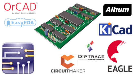
Today, dozens of PCB design software can be found in the market with familiarity. This article will help you in selecting PCB design software and compare these parameters among the most commonly used PCB Design Software.
https://pcbdesignworld.com/article/which-pcb-software-should-you-choose%3F%E2%80%93selection-criteria-and-available-options
0 notes
Text
Wants to start your Career in PCB Designing....
wait a minute, .. First, you need to understand all the basics and terminologies used in PCB Designing...
Don't worry!!! we are going to help you in PCB Designing..Just check out https://pcbdesignworld.com/article/what-is-pcb-types-of-pcb-basics

1 note
·
View note