
Based on China to serve the world ABOUT HITECHPCBA Hitechpcba is a wоrld-lеаding PCB Manufacturing & PCB Assembly company with more than 20 years experience in the electronics manufacturing industry. We focus on PCB Design, PCB Layout, Circuit board fabrication, Turnkey PCB assembly, and electronic parts sourcing services.https://www.hitechpcba.com/
Don't wanna be here? Send us removal request.
Statistics
We looked inside some of the posts by roger-hitechpcba666 and here's what we found interesting.
Average Info
Notes Per Post
1
Likes Per Post
1
Reblog Per Post
0
Reply Per Post
0
Time Between Posts
7 days
Number of Posts By Type
Text
17
Last Seen Tumblr Blogs


Fun Fact
Tumblr has 411 employees.
Text
Professional high frequency pcb board manufacturer in China Made by Hitech Circuits Co., Limited
Hitech is a professional high frequency pcb board manufacturer in China, our high frequency PCBs (RF PCB) are widely used in wireless networks, wireless communications and satellite communications, in particular the popularity of 4G,5G networks exacerbate the market demand for the product on the RF PCB. For some special high-frequency PCB materials ( such as: Teflon PCB material, Rogers PCB materials were ), we have sufficient inventory. If you are looking for high frequency pcb manufacturer in China, please contact [email protected], we won’t let you down.
What is a high frequency PCB board
High frequency PCB boards are special circuit boards with higher electromagnetic frequencies. Generally speaking, high-frequency can be defined as frequencies above 1GHz. Its various physical properties, accuracy, and technical parameters require very high requirements, and are often used in automotive anti-collision systems, satellite systems, radio systems and other fields.
With the rapid development of science and technology, more and more equipment designs are applied in the microwave frequency band (>1GHZ) and even in the millimeter wave field (30GHZ), which also means that the frequency is getting higher and higher, and the requirements for the circuit board are getting higher and higher. For example, the substrate material needs to have excellent electrical properties, good chemical stability, and the loss on the substrate with the increase of the power signal frequency is very small, so the importance of the high-frequency PCB board is highlighted.
High frequency PCB board production process
NPTH PTFE board processing flow
Cutting-drilling-dry film-inspection-etching-erosion inspection-solder mask-characters printing-spray tin-forming-testing-final inspection-packaging-shipment
PTH PTFE board processing flow
Cutting-drilling-hole treatment (plasma treatment or sodium naphthalene activation treatment)-copper immersion-board electricity-dry film-inspection-diagram electricity-etching-corrosion inspection-solder mask-character printing-spray tin-forming-test-final Inspection-packaging-shipment
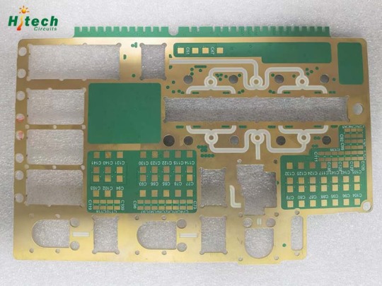
General specification for high frequency pcb (Rogers PCB, Teflon PCB, RF PCB)
Layer count: 1-6 Board thickness: 0.2-5.0mm Copper thickness: 0.5-3 oz Dielectric Constant(DK): 2.2-10.3 Min trace width/spacing: 4/4mil Min drill hole size: 0.15mm Surface treatment: HASL, HASL Lead free, Immersion Gold/Tin/Silver, OSP, etc. Material available: Teflon pcb material, Rogers pcb material, Taconic pcb material, Arlon pcb material, etc.
Advantages of high frequency PCB board
1. High efficiency
High-frequency PCB boards with small dielectric constants will have very low losses, and advanced induction heating technology can achieve the target heating requirements with very high efficiency. Of course, while focusing on efficiency, it also has the characteristics of environmental protection, which is very suitable for the development direction of today’s society.
2. Fast transmission speed
The transmission speed is inversely proportional to the square root of the dielectric constant, which means that the smaller the dielectric constant, the faster the transmission speed. This is the advantage of the high-frequency printed circuit board. It uses special materials, which not only guarantees the low dielectric constant, but also maintains the stable operation, which is very important for signal transmission.
3. Large degree of controllability
High frequency PCB board is widely used in various industries that require precision metal material heating treatment. In the process of its field, not only can heating of different depth components, but also focus on heating according to local characteristics, whether it is surface or deep level; centralized or decentralized heating methods can be easily completed.
4. Strong tolerance
Dielectric constant and medium have certain requirements on the environment, especially in the south, where wet weather will seriously affect the use of circuit boards. High-frequency circuit boards made of materials with extremely low water absorption can challenge such an environment. At the same time, they also have the advantages of resistance to chemical corrosion, moisture, high temperature, and great peel strength, allowing high-frequency circuit boards to exert powerful performance .
Applications of high frequency PCB board
Mobile communication products.
Power amplifier, low noise amplifier, etc.
Passive components such as power splitters, couplers, duplexers, filters, etc.
Automobile anti-collision systems, satellite systems, radio systems and other fields.
Why lots of industry Choose Rogers PCB
Rogers PCBs can be trusted as there are lesser products to serve at its level in conventional PCBs.
It is also reliable in terms of their service criteria because they offer samples so that anyone can understand the effectiveness and efficiency before finalizing. This puts ease among the customers to choose Rogers PCB.
The moisture absorption feature is not served by the ordinary PCBs which is also a reason for Rogers PCBs increasing popularity. These characteristics are appropriate for being used in every kind of environment and weather conditions by ensuring lesser chances of malfunctions. In addition, Rogers PCB is resistant to several types of chemicals so that it can be used in almost all the industries without any pressure.
FAQs about High-Frequency PCBs
1. Can High-Frequency PCBs be customized for specific applications?
Absolutely! High-Frequency PCBs can be customized in terms of layout, material choice, and specifications to meet the unique requirements of different applications. Whether you need a board for a satellite communication system or a medical imaging device, customization ensures that your PCB will deliver optimal performance.
2. How do High-Frequency PCBs compare to standard PCBs?
High-Frequency PCBs are specifically engineered for high-speed applications, where they outperform standard PCBs by ensuring higher signal integrity and reduced electromagnetic interference. This makes them indispensable in advanced electronic systems where performance and reliability at high frequencies are critical.
3. How are High-Frequency PCBs tested for quality?
High-Frequency PCBs undergo rigorous testing, including signal integrity analysis, thermal cycling, and electromagnetic compatibility (EMC) testing. These tests ensure that the PCBs meet the highest standards of quality and performance before they are deployed in critical applications.
4. What design considerations are important for High-Frequency PCBs?
Key considerations include selecting the appropriate substrate material, designing for minimal electromagnetic interference, optimizing the layout for signal integrity, and ensuring thermal management. Attention to these details is crucial for maximizing the performance of high-frequency applications.
5. Where can I get High-Frequency PCBs manufactured?
You can get High-Frequency PCBs manufactured at specialized companies like HiTech Circuits, which offer extensive experience and expertise in producing high-quality, high-performance PCBs tailored to your specific needs.
0 notes
Text
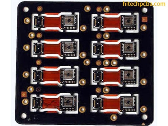
Good Performance Rigid flex PCB Board Made in China
Hitech Circuits Co., Ltd is a professional rigid flex pcb printed circuit board manufacturer & supplier from China, our rigid-flex pcb board saves production time, minimize product size and improve equipment reliability, suitable for mobile phones, digital cameras, medical devices, smart control system, and other smart smart devices. If you are looking for long term rigid flex pcb and other pcb products partner in China, Hitech is the right company you are looking for, don’t hesitate to contact [email protected] if you need any help from us.
What is rigid flex pcb board?
Rigid-flex PCB board, it is a circuit board that combines flexible and rigid circuit board technology in the application. Most rigid-flex boards are composed of multiple layers of flexible circuit boards, which are attached to one or more rigid boards from the outside and/or from the inside, depending on the design of the application. The flexible substrate is designed to be in a constant deflection state, and is usually formed as a deflection curve during rigid flex pcb manufacturing or assembly.
Hitech rigid flex pcb manufacturing process
After the production of FPC flexible boards is completed, the production of Hitech rigid flex pcb boards can be completed through the following processes.
1. Punching
Drill holes on FR4 and PP film, and the design on the alignment hole is not the same as the general through hole. After the punching is completed, browning is required.
2. Riveting
Laminate copper clad laminates, PP adhesives, and FPC circuit boards and place them neatly. The original old process is to laminate and pressing step by step, but it is a waste of time. After many attempts, we found that the stacking process can be completed once.
3. Laminate
This is a relatively complete step in the production of rigid-flex pcb board. Most of the materials are integrated for the first time. First, the bottom layer is copper clad laminate and PP film, above are the FPC flexible board produced in the previous process, and a PP film is placed on the FPC flexible board, then place the last layer of copper clad laminate. All materials to be laminated are placed in order and pressed together.
4. Trimming
That is to remove the part of the circuit board where there is no circuit at the edge of the circuit board currently and in the future. Afterwards, it is necessary to measure whether the material has excessive expansion and contraction. Because the PI used in the production of flexible boards is also expansion and contraction, this has a very large impact on the production of circuit boards.
5. Drilling
This step is the first step to turn on the entire circuit board, and the production parameters should be produced according to the design parameters.
6. Desmear
First, remove the scum generated by the drilling of the circuit board, and then use plasma cleaning to clean the through holes and the board surface.
7. Immersion copper
This step is the process of electroplating through holes, also known as hole metallization. Realize through-hole power conduction.
8. Plate plating
Partially electroplating copper on the upper surface of the electroplating hole makes the copper thickness above the through hole exceed a certain height of the copper clad board surface.
9. Outer dry film positive film production
The same as the production process of the anti-corrosion dry film of the FPC board, the circuit to be etched on the copper clad board is made. After the development is completed, check the circuit.
10. Graphic plating
After the initial copper sinking, pattern electroplating is performed, and the current time and copper plating wire are used according to the design requirements to reach a certain electroplating area.
11. Alkaline etching
12. Print solder mask
This step has the same effect as the FPC board protective film. We see that the PCB rigid board is generally green. This step is generally called green oil printing. After the printing is completed, the inspection is carried out.
13. Open the cover
Cover opening, which is the area where the FPC board is located, but the area not needed by the rigid board is laser cut to expose the FPC board.
14. Curing
It is also a baking process.
15. Surface treatment
Generally, at this time, a rigid-flex PCB board has been manufactured, and only the metallization treatment is required on the surface of the circuit board, which can play a role in preventing wear and oxidation. Generally, this process is to soak the circuit board in a chemical solution, and the metal elements in the solution are densely distributed on the circuit board circuit.
16. Characters printing
The positions of the parts to be assembled and some basic product information are printed on the rigid-flex board in the form of characters.
17. Test
This is a process of checking whether the circuit board is qualified. The test items are tested for electrical properties according to customer requirements. The tests generally include impedance test, open and short circuit test and so on.
18. Final inspection
19. Packaging and shipping
There are many ways to package circuit boards. Generally, Hitech use packaging bags to separate them, and then use a vacuum packaging machine to vacuum package the rigid-flex PCB boards .
The advantages of rigid-flex PCB board
1). It can effectively save the space on the circuit board and eliminate the use of connectors
Because the FPCB and rigid pcb board has been combined, the space that originally needed to use the connector can be saved. For some circuit boards with high-density requirements, less connectors will be better. In this way, it also saves the cost of parts using the connectors. In addition, the space between the two boards can be made tighter by eliminating the need for connectors.
2). The signal transmission distance is shortened and the speed is increased, which can effectively improve the reliability
The traditional signal transmission through the connector is “circuit board→connector→flexible pcb board→connector→circuit board”, while the signal transmission of the rigid-flex PCB board is reduced to “rigid circuit board→flexible pcb board→rigid circuit board”, signal transmission distance between different media is shortened, and the problem of signal transmission attenuation between different media is also reduced. Generally, the circuit on the PCB board is made of copper, while the contact terminal of the connector is gold-plated, and the solder pin is fully tin-plated. Moreover, solder paste is required to be soldered on the circuit board, and the signal transmission between different media will inevitably be attenuated. If you switch to a rigid-flex PCB board, these media will become less, and the signal transmission ability can be relatively improved. For some products that require higher signal accuracy, it helps to improve their reliability.
3). Simplify product assembly and save assembly time
The use of a rigid-flex PCB board can reduce the man-hours for SMT parts, because the number of connectors is reduced. It also reduces the man-hours for assembly of the whole equipment, because it eliminates the assembly action of inserting the FPC board into the connector. It also reduces the cost of parts management and inventory, because the required parts is reduced, so the management cost becomes less.
The disadvantages of rigid-flex PCB boards
The biggest disadvantage of the rigid-flex PCB board is that the price of “rigid-flex PCB board” is more expensive, and it may be nearly double the original price of pure “FPC board + rigid PCB board”, but if the price of the connector and processing cost is deducted, the price may tend to be the same, and the detailed cost may have to be actuated to have a clearer outline.
Another disadvantage is that it may need to use a carrier to support the part of the FPC board for both the production and the furnace, which invisibly increases the assembly cost of the SMT.
1 note
·
View note
Text

Turnkey Electronics Assembly Services in China with High Quality and Competitive Price
Hitech Circuits provides a full turnkey solution to all of your electronics assembly requirements. From PCB fabrication, components sourcing, pcb assembly to full box build assembly we can provide a full electronics manufacturing services solution to your electronics manufacturing requirements. Using surface mount production machinery consisting of three surface mount technology placement machines, a screen printing machine and a 10 zone reflow oven, accompanied by offline bench assembly, visual inspection and rework stations, we can offer small to medium volume services for all your pcb assembly requirements. We offer pcb assembly, visual inspection, functional and electronics testing and programming services. We can source all components, bare pcbs and production stencils. If you would like to work with an electronics manufacturer you can trust then please get in touch.
Also, we offer both turn-key and partial turn-key PCB Electronics assembly.
For full turn-key services, we manage and produce everything including manufacturing the circuit boards, finding & ordering PCB components, quality inspection & testing and the final product assembly.
Pls send PCB files to [email protected] to get a quote now!
Advantages of Full Turnkey PCB Assembly Services
• Shorter Lead Time
As a fundamental form of electronic assembly, PCB assembly primarily contains three phases: PCB fabrication, components procurement and PCB assembly. Traditionally, you should quote and confirm design files with sales and engineers working for your PCB manufacturer, then components distributors and finally PCB assemblers. Such series of quotations and confirmations just need your time spent in contacting with different partners. If those partners are from different countries, you have to overcome some problems such as time zone, communication habits etc. Full-turnkey PCB assembly, however, is a highly-efficient form of electronic assembly. As soon as full-turnkey PCB assembly is determined, an overall assembly quotation and indispensible issues prohibiting smooth manufacturing will be raised so that three times of communication have been cut to one time with electronic assembly efficiency dramatically improved in Hitech Circuits Co., Limited.
• Lower Cost
Another advantage of full-turnkey PCB assembly service is overall cost reduction. Pack-up service is usually cheaper than separate ones as far as electronic assembly is concerned. At least, freight fee will be saved because you don’t need to get manufactured PCB boards and electronic components delivered to assembly workshop. Moreover, components procurement may get easy and customer-friendly because experienced electronic assemblers are usually able to provide reliable components with relatively low cost based on their long-term cooperation with parts manufacturers or distributors.
• Transparent Monitoring
When it comes to electronic assembly process, it’s significant yet difficult to monitor your products’ manufacturing stage as it is totally related with your products’ performance and time to market. Full-turnkey PCB assembly allows engineers at each stage to be aware of what they’ve accomplished and to better understand their status for better performance of final products.
Who Can Benefit Most From Our Turnkey PCB Assembly Services?
Now that full turnkey PCB assembly allows PCB designers to make better use of their time to focus more on PCB design, it works perfectly on companies striving for frequent upgrading and refreshing of products. They need to dig into deeper market by providing multiple creative electronic products and they strongly call for a steady and smooth electronic assembly process.
Turnkey printed circuit board assembly is also an ideal electronic assembly solution for small businesses or startup companies that want to bring smaller quantities of assembled PCBs to market without having to invest in or carry an extensive inventory. It also offers a more cost-effective, efficient means of assembling and testing PCB prototypes for new products. In addition, quick-turn PCB assembly service makes sense for any company that needs to receive their circuit boards with the shortest possible lead time.
0 notes
Text
Express Prototype PCB Assembly by Famous Hitech Circuits Co., Limited
Hitech express prototype PCB assembly manufacturing is a specialized service that enables us to take complicated PCB fabrication, components souring and prepare them for assembly and testing. As the top PCB manufacturer in the China, Hitech Group can fulfill your prototype and production needs. We understand that bringing a product to market in a timely and cost- effective manner can mean everything in business. Our quality, experience, service and pricing combine to become your efficient and reliable electronic supplier. We use the latest equipment to assembly complex PCBs as promptly as possible – often with 24 hours. We are setup specifically for deal with fast turn electronics assembly and all the issues that go hand in hand with the process, giving us an upper hand over most manufacturers, our team is capable of manufacturing prototype printed wiring board assembly volumes of 1-50 pieces.
Our knowledgeable and experienced staff have the know-how and equipment to be able to deal with any project you care to send our way – no job is too demanding. We can guarantee we will deliver exactly what you need with both speed and quality, so you can rest easy knowing you’re in good hands.
please send to project files to [email protected] to get a quote.
Benefits of PCB Prototype Assembly
The reason for ordering a PCB prototype, it’s because is that you want to quickly assess how well your PCB design is going to work. You cannot do that without going through the board assembly process. Fortunately, HitechPCB can do your PCB prototype assembly in-house, so you can find out quickly just how well your assembled PCB prototype works.
There’s no need to fabricate it here and then search for a specialist in prototype PCB assembly. That would take too long and defeat the purpose of making a PCB prototype in the first place. Work with HitechPCB, and let us do it all for you – fast.
PCB Prototype Assembly Featuring Our Equivalently High Quality Standards
While prototype assembly typically consists of a limited production run, we bring the same high level of quality and care to the process as with our full-production assembly projects. We utilize the same resources and personnel to ensure the best possible results. Our capable team is fully qualified to handle every aspect of the process, including the procurement of PCB parts and electronics components, circuit boards fabrication, PCB assembly manufacturing and quality control. We will also follow your original PCB prototype design to the letter. We won’t make any modifications or alterations without your approval. Our services include Design for manufacture (DFM) ability and Design for Testing (DFT) to ensure your PCBA prototype will meet your exact design specifications. We can even assemble prototypes for high-density FR-4 circuit boards.
Prototype PCB Assembly at Competitive Prices
HitechPCB offers a number of ways to minimize your PCB prototype assembly costs. We are the best possible option when it comes to all of your PCB solutions including printed circuit board fabrication, PCB components sourcing and prototype circuit board assembly needs. Because we do everything in-house with our team of highly-trained engineers and design experts, you know you’ll get a smooth and efficient flow of communication that will result in you getting just the prototypes you want. You or your management team won’t get tied up in logistics trying to get a design company to communicate with a manufacturer. To get PCB prototype assembly quote for your custom PCB project, please send related circuit spec and BOM files to us. We will give the PCB Assembly price within 24 hours.
PCB Assembly Quote within 12 holes for urgent project
A PCB assembly is a circuit board with all the necessary components. Various factors like the number of different parts, type of PCB assembly, and services determine how you get your PCB assembly quote. Usually, lots of suppliers quote PCBA need more than 5 days, but we have lots of experienced staff, for PCB assembly quote can send to you within 12holes for urgently project quote.
Hitech Group offers SMT Assembly services for our Printed circuit boards customers. We will quote you in a short time, we will follow your BOM list to purchase components. We provide competitive prices for PCBA services like our PCBs. All your projects can be done under one roof: PCB manufacturing, assembly, PCBA Testing!
To get a quick turnaround PCB assembly quote , you need provide these data.
Gerber files, BOM list, Q’ty, testing program, request lead time, shipping address, etc.
Welcome to choose Hitech Group as your PCB, Electronic assembler, PCB assembly manufacturer, for quick turnaround lead time of bare PCB, please review the link.
0 notes
Text
Low & High-Volume Electronics Assembly in Shenzhen China
We provide quick-turn PCBA prototype, from prototype to low-volume and production Electronics assembly manufacturing with surface-mount (SMT), through-hole (THT) and mix components. We offer turn-key (just send us the Gerber and BOM files), consignment (you supply all parts) and various components purchase options to help you reduce cost and wait time. Our quick-turn circuit board assembly prototyping service can assemble your boards within 24 hours. We can handle small quantity as well as volume productions. All our services are at a very competitive price and with 100% satisfaction guarantee.
Pls send PCB files to [email protected] to get a quote now!
Also, if your business is involved in applications that require high-volume PCB assembly, the company to contact is HitechPCB, because we’re a complete turnkey solution for printed circuit boards assembly, we are ideally suited for bulk PCB assembly orders. Our state-of-the-art equipment, large facility and wide range of highly-qualified experts give us the capability of high-volume PCB assembly of up to 9,000,000.
We are also the perfect source if you’re looking for large-order PCB assembly on a budget. Because of our high level of efficiency and more than 10 years of experience with printed circuit board manufacturing and electronics assembly, we offer large printed circuit board orders at surprisingly competitive prices compared to other PCB manufacturers or PCB assembly companies.
Our large order PCB assembly process starts with a tested and practiced set of workflow guidelines for every phase of the process, from pre-order PCB design consultation with professional veteran engineers to PCB fabrication, components sourcing, PCB assembly, PCBA testing, PCBA inspection, PCBA packing and shipping all under the auspices of a highly-skilled production staff. You can be confident that n
HitechPCB is a proficient, electronic contract manufacturer (ECM) with a focus on low-volume, turn-key, circuit board assembly services. The turn-key service uses Design for Manufacturing (DFM) and Design for Testing (DFT) services. Small volumes are usually defined as orders less than 6,000 circuit boards.
Design for Manufacturing (DFM) Service
To avoid several engineering issues that may hamper the fabrication process, which could possibly cause delivery delays, we use a Design for Manufacturing (DFM) service that functions as a method of scrutinizing the quality of the customer’s engineering documents such as Gerber files, bill of materials, assembly drawings, and circuit diagrams. Additionally, it will panel the circuit boards, examine your components list to check its accuracy prior to the components being ordered, and recommend a solder mask to obtain high output rates. HitechPCB is able to give price discounts to its consumers due to incorporating its DFM service into its circuit board assembly.
Design for Testing (DFT) Service
To facilitate your circuit board testing process and provide suggestions on where to place test points throughout your circuit board, HitechPCB employs a Design for Testing (DFT) service. References regarding probe types, fixtures, and testing limitations are provided by this service. The DFT service will validate that your testing requirements, problem detection processes, problem-solving instructions, and other references are well-designed.
0 notes
Text
Professional Printed Circuit Board Assembly Services by Hitech Circuits Co., Limited
Hitech is an expert PCB manufacturing & assembly company that proudly supplies PCB assembly solutions to businesses of all sizes in China. Our industry-leading PCB assembly processes create PCBs of the highest quality. Our expert team is made up of in-house trained professionals who have the experience and expertise to create dependable PCBs and utilise our PCB assembly technology. Through our strong network of well-proven PCB assembly and manufacturing partners, we can provide the most advanced and nearly limitless capabilities for your prototype or production PCB application. Save yourself the trouble that comes with the procurement process and dealing with multiple components vendors. Our experts will find you the best parts for your final product.
Printed Circuit Board Assembly Service ( PCB Files & BOM List, please send to [email protected] ( Fast Quote )
Printed Circuit Board Assembly is a process that requires knowledge not just of Printed Circuit Board components and assembly but also of printed circuit board design, Printed Circuit Board fabrication and a strong understanding of the final product. Circuit board assembly is just one piece of the puzzle to delivering the perfect product the first time.
Printed Circuit Boards (PCBs) are across many industrial and consumer electronics. The versatility of PCBs comes from their lightweight, compact, and flexible construction, which can be adapted to suit circuits of any complexity. Though PCBs are relatively commonplace, their complexity makes it critical to source new circuit boards from reliable suppliers. Printed Circuit Board Assembly services harness these complexities.
Hitech Group offers comprehensive Printed Circuit Board Assembly services that help our customers fully realize their designs. We have extensive experience working with customers in a broad range of highly innovative industries, including Communication, Automotive, Industrial control, Medical equipment, Oil & Gas, Security, and so on.
Printed Circuit Board Assembly Process
The PCB assembly process can look very different depending on the type of PCB and the order volume. Our PCB assembly process include any of the following steps, depending on the client’s needs:
Automated Assembly Automated PCB assembly is ideal for components that are difficult to solder by hand and high-volume production runs. It is the fastest and most efficient means of producing consistent circuit boards.
Reflow Reflow soldering is the most common method used for efficiently soldering SMT-mounted components. The process uses a reflow oven to melt solder onto a pre-heated and pre-soaked PCB.
Wave Solder Wave soldering is another efficient method that involves applying flux to an entire PCB surface, heating the board, and then applying molten solder to the whole heated board.
Selective Solder Selective solder is a more precise variation of wave soldering used to apply flux locally rather than the entire PCB. Instead of using a “wave” of molten solder, it uses nozzles to apply solder exactly where needed.
Hand Insertion and Soldering Hand insertion and soldering may be used when project constraints require manual through-mounting.
Point-to-Point Wiring Point-to-point wiring is a labor-intensive manual assembly method that involves hand-mounting and soldering all components on a circuit board. This process is used as an alternative to PCBs in specific applications, including repairs to vintage electronics.
Automated Optical Inspection (AOI) This automated inspection process uses cameras to scan the PCB for defects and quality issues.
Solder Paste Inspection (SPI) The SPI process closely inspects solder paste deposition before part placement.
These additional services represent one of our most significant advantages over our competitors. Many companies cannot provide the X-Ray capabilities or ionograph testing necessary for industries requiring immaculate boards. For example, our medical clients leverage our ability to measure contamination down to ppm on a single square centimeter.
Ball Grid Arrays (BGA) Ball Grid Arrays are used on highly complex PCBs to mount microprocessors and other integrated circuit components. BGAs provide more interconnection pins to facilitate faster and more reliable component connections. While BGAs and micro-BGAs provide superior performance, they are also exceedingly difficult to solder. Incorporating BGAs and micro-BGAs into your PCB assembly requires partnering with an expert Electronics Manufacturing Services provider like Hitech Group.
For more, please visit at https://hitechcircuits.com/pcb-assembly/printed-circuit-board-assembly-services/
0 notes
Text

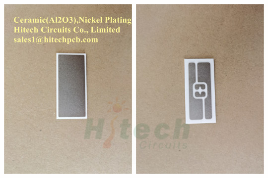
Ceramic PCB Special PCB with Big Function and Use made by Hitech Circuits
We are a professional ceramic pcb manufacturer, supplier from China, we mainly supply high quality Alumina (Al2O3) Ceramic PCB, Aluminum Nitride (AIN) Ceramic PCB board and IGBT Ceramic PCB. Our ceramic printed circuit boards features of high pressure, high insulation, high temperature, and high reliable and minor volume electronic products, Hitech is your best choice for ceramic PCB boards and needs.
Pls send PCB files to [email protected] to get a quote now!
What is ceramic pcb board
Ceramic pcb boards are actually made of electronic ceramics as the basic material and can be made in various shapes. Among them, the characteristics of high temperature resistance and high electrical insulation of ceramic circuit boards are the most prominent. The advantages of low dielectric constant and dielectric loss, high thermal conductivity, good chemical stability, and similar thermal expansion coefficient to components are also very significant.
Different types of ceramic pcb
Ceramic PCB is widely used in power electronics, electronic packaging, hybrid microelectronics and multi-chip modules due to its excellent thermal conductivity and air tightness. But not everyone is clear about the classification. Many manufacturers think ceramic PCBs are expensive and fragile as soon as they hear about ceramic PCBs. Yes, this is indeed a shortcoming of ceramic PCBs, but not all ceramic PCBs are like this. Today we will tell you about the different types of ceramic PCBs.
Al2O3 ceramic PCB
Al2O3 ceramic PCB ( alumina ceramic PCB) refers to various ceramic PCBs with Al2O3 as the main raw material and an Al2O3 content of more than 75%. It has a rich source of raw materials, with advantages of low price, high mechanical strength and hardness, good insulation performance, good heat shock resistance, good chemical resistance, high dimensional accuracy, and good adhesion to metals. It is a ceramic substrate material with good comprehensive performance. Currently used Al2O3 ceramic substrates, the content of Al2O3 accounts for 85% to 99.5%. Among them, 96% Al2O3 ceramic PCB is widely used in the production of thick film circuit substrates and chip devices. The thermal conductivity of Al2O3 at room temperature is 29W/(m·K), which is close to the thermal conductivity of steel; with the increase of Al2O3 content, the electrical insulation performance and thermal conductivity of Al2O3 ceramic PCB will increase, but At the same time, it will also lead to an increase in the firing temperature, an increase in energy consumption, a large loss of kiln furniture, and an increase in manufacturing costs.
SiC ceramic PCB
The thermal conductivity of SiC ceramic PCB is very high, 100~490W/(m·K) at room temperature, and it is related to the purity of SiC crystals. The higher the purity, the greater the thermal conductivity; the oxidation resistance is good, and the decomposition temperature is above 2500℃, it can still be used at 1600℃ in an oxidizing atmosphere; the coefficient of thermal expansion is also low, and it is close to Si, with good electrical insulation performance; SiC has a Mohs hardness of 9.75, second only to diamond and cubic BN, and has high mechanical strength. SiC ceramics have strong covalent bond characteristics and are difficult to sinter. Usually, a small amount of boron or aluminum oxide is added as a sintering aid to increase the density. Experiments show that beryllium, boron, aluminum and their compounds are the most effective additives, which can make SiC ceramics denser than 98%.
BeO ceramic PCB
BeO has a brazine structure, in which oxygen ions are arranged in a hexagonal close-packed manner to form a hexagonal lattice. The general oxide is usually an ionic compound, but BeO has a strong covalent bond and an average molecular weight of only 12. Because of its good electrical properties, luminescence and photochemical properties, high mechanical strength, low dielectric loss, etc, it become one of the materials that people pay attention to.
AlN ceramic PCB
AlN ceramic PCB (aluminum nitride ceramic) is a new type of high thermal conductivity ceramic packaging material. It has been extensively studied in the 1990s and gradually developed. It is currently generally considered to be a promising electronic ceramic packaging PCB. AlN material has high thermal conductivity, excellent dielectric properties, high electrical insulation strength, stable chemical properties, strong corrosion resistance, and good mechanical properties. In particular, its thermal expansion coefficient matches with silicon, which makes it an ideal semiconductor packaging substrate materials and have been widely used in integrated circuits, microwave power devices, millimeter-wave packaging, high-temperature electronic packaging and other fields.
Ceramic PCB for IGBT Module
IGBT stands for insulated-gate bipolar transistor. It is a bipolar transistor with an insulated gate terminal. The IGBT combines, in a single device, a control input with a MOS structure and a bipolar power transistor that acts as an output switch. IGBTs Ceramic PCB are suitable for high-voltage, high-current applications. They are designed to drive high-power applications with a low-power input.
IGBT, or Insulated Gate Bipolar Transistor, is a BJT transistor with a MOS Gate, or we can say an IGBT module is the combination of a BJT and a MOS Gate. An IGBT chip is small in size, but it can control electrical energy transmission and achieve 100,000 times of current switch at ultra-high voltages of 650 million V in only 1 second.
IGBT modules have been applied in automotive, industrial, aerospace, consumer electronics, and many other industries for many years. But how to optimize the thermal dissipation of an IGBT package so the module can work at a higher power? If thermal can dissipate more quickly, the IGBT module can have more advanced applications. For this purpose, engineers are using ceramic PCBs for IGBT packaging.
Ceramic PCBs dissipate thermal from IGBT chip to the outer packaging
You may ask, how much thermal does an IGBT module generate when it works? It is equal to the heat generated by 100 electric furnaces. So much thermal has to be dissipated immediately from the IGBT chip and leads to the application of ceramic PCBs.
How does a ceramic PCB protect the IGBT module from the heat? In an IGBT module, a ceramic PCB is placed under the IGBT chip, or we can say that the chip is assembled on the ceramic circuit board. The ceramic PCB connects and supports the chip and dissipates thermal quickly from it to the outer packaging. In this way, the chip is protected from the influence of thermal.
Why Ceramic PCBs can be used for IGBT thermal dissipation
There are alumina (Al₂O₃) PCBs, aluminum nitride (AlN) PCBs, and silicon nitride (Si₃N₄) PCBs used for thermal dissipation of IGBT modules.
Why ceramic PCBs can dissipate thermal effectively for the IGBT module? Because ceramic materials have good properties of thermal dissipation and electrical insulation. Unlike aluminum substrate PCBs, ceramic PCBs do not use an insulation layer that hinders thermal dissipation. During the ceramic PCB manufacturing process, the copper-clad is directly bonded onto the ceramic substrate at high temperatures under high pressures. Then the circuit layer is manufactured by the photoresist coating method. When the circuit board is manufactured, the IGBT and other components are mounted on the board. Ceramic materials have ultra-high insulation and can withstand breakdown voltage up to 20KV/mm. The thermal conductivity of alumina PCBs is 15-35W/mK, aluminum nitride PCB 170-230W/mK, and silicon nitride PCB 80+W/mK. On the contrary, an aluminum PCB has thermal dissipation of only 1-12W/mK.
Usages and applications of ceramic printed circuit boards
Ceramic printed circuit boards have a wide range of applications and can be used in the LED field, solar panel components, high-power power semiconductor modules, semiconductor refrigerators, electronic heaters, power control circuits, power hybrid circuits, smart power components, high-frequency switching power supplies , solid state relays, automotive electronics, communications, aerospace and military electronic components.
Advantages of ceramic PCB boards
Higher thermal conductivity
More matching thermal expansion coefficient
Stronger and lower resistance metal film
The solderability of the substrate is good, and the use temperature is high
Good insulation
Low high frequency loss
High-density assembly is possible
It does not contain organic ingredients, is resistant to cosmic rays, has high reliability in aerospace and has a long service life
The copper layer does not contain an oxide layer and can be used for a long time in a reducing atmosphere
Disadvantages of ceramic pcb boards
1. Fragile This is one of the most important shortcomings. At present, only small-area ceramic printed circuit boards can be produced.
2. Expensive There are more and more requirements for electronic products. Ceramic circuit boards only meet the requirements of some relatively high-end products, and low-end products will not be used at all.
0 notes
Text
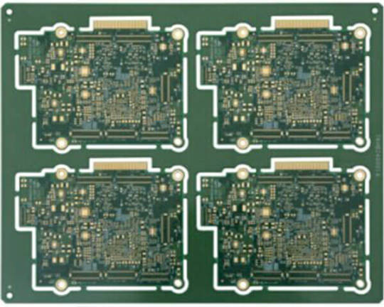
High Density Interconnect PCB with Good Performance and Quality
HDI pcb is the abbreviation for High Density Interconnect pcb or High Density pcb. An HDI PCB is defined as a printed circuit board with a higher wiring density per unit area than a conventional PCB. Hitech Circuits Co., Limited is a professional high density interconnect pcbs, hdi pcb board manufacturer, supplier and design company from China, if you are looking for reliable high density interconnect PCb board partner from China, please don’t hesitate to contact [email protected].
What is a high-density interconnection PCB board
HDI is the abbreviation of High Density Interconnection, which is a kind of technology for the production of printed circuit boards. High density interconnection PCB board is a circuit board with a relatively high line distribution density using micro-blind and buried via technology.
HDI includes the use of fine features or signal traces and spaces of 0.003” (75 µm) or less and laser-drilled blind or buried microvia technology. Microvias allow the use of micro-interconnects from one layer to another within a PCB utilizing a smaller pad diameter creating additional routing density or reducing form factor.
HDI pcb board is a compact product designed for small-capacity users.
Advantages of high-density interconnected PCB boards
It can reduce the cost of PCB: When the density of PCB increases to more than eight-layer board, it is manufactured by HDI, and its cost will be lower than that of the traditional complex pressing process.
Increase circuit density: has better interconnection than that of traditional circuit boards and parts
Conducive to the use of advanced construction technology
Have better electrical performance and signal accuracy
Better reliability
Can improve thermal properties
It can improve radio frequency interference ( RFI ), electromagnetic wave interference ( EMI ), electrostatic discharge ( ESD )
Increase design efficiency
Disadvantages of high-density interconnected PCB boards
The value of NDI impedance focuses on pattern transfer (complexity of patterns) and pattern electroplating process.
The quantity and quality are abnormal, especially the high-density circuit part of the HDI PCB board has a slower etch rate than the isolation line, which causes the isolation line to be over-etched.
When the entire HDI board is etched after electroplating, a large area of copper on the PCB circuit board will be etched away, which increases the production cost. At the same time, a large amount of copper ions enter the waste liquid after etching, causing environmental pollution and difficulty in recycling.
High-density interconnection PCB board Vs ordinary PCB board
Ordinary PCB board is mainly FR-4, which is laminated with epoxy resin and electronic grade glass cloth. Generally, traditional HDI PCB board uses backed copper foil on the outer surface, because laser drilling cannot penetrate the glass cloth, glass fiber-free backed copper foil is generally used. However, the current high-energy laser drilling machine can penetrate 1180 glass cloth. This is no difference from ordinary PCB board materials.
Applications of high-density interconnected PCB boards
While electronic design is constantly improving the performance of the whole equipment, researchers are also working hard to reduce its size. In small portable products ranging from mobile phones to smart weapons, “small” is an eternal pursuit. High-density interconnection (HDI PCB) technology can make terminal product designs more compact, while meeting higher standards of electronic performance and efficiency. HDI PCB board is widely used in mobile phones, digital cameras, MP3, MP4, notebook computers, automotive electronics, IC carrier boards and other digital products, among which mobile phones are the most widely used.
High density PCB is used extensively in applications and industries including
Cell phone
GPS
Telecom
Semiconductor
Automotive
Military
Medical
Instrumentation
Note book computers
IC Carrier board
Healthcare
FAQs for Hitech Circuits on HDI PCBs
1. What types of HDI PCBs are available at Hitech Circuits? Hitech Circuits offers a range of HDI PCBs, including those with through vias from surface to surface, with buried vias and through vias, sequential lamination with various materials, and with passive substrate constructions having no electrical connection. Each type caters to specific design and performance requirements.
2. Can Hitech Circuits accommodate custom HDI PCB designs? Absolutely! Hitech Circuits specializes in custom HDI PCB designs tailored to meet unique project requirements. Our team works closely with clients to understand their needs and deliver high-quality, precise PCBs that fit their specifications.
3. What materials are used in the manufacturing of HDI PCBs? HDI PCBs at Hi-Tech Circuits are made from various high-quality materials, including FR-4, high-frequency materials (such as Rogers and Taconic), and flex and rigid-flex materials. Material selection depends on the application’s requirements, such as thermal management, electrical performance, and mechanical durability.
4. How does Hitech Circuits ensure the quality of their HDI PCBs? Quality assurance is paramount at Hitech Circuits. We employ stringent quality control processes at every manufacturing stage, from design and material selection to fabrication and testing. Our HDI PCBs undergo multiple quality checks, including electrical testing, visual inspection, and automated optical inspection (AOI) to ensure they meet the highest standards.
5. What are the lead times for HDI PCB production? Lead times for HDI PCB production can vary based on the complexity of the design and the quantity required. Generally, prototype orders can be completed within a few days to two weeks, while larger production orders may take several weeks. We strive to meet our clients’ deadlines and can provide more specific timeframes upon order placement.
6. Are there any design guidelines for HDI PCBs I should follow? Yes, Hitech Circuits provides detailed design guidelines for HDI PCBs, which include recommendations on trace width, spacing, via sizes, and layer stacking. These guidelines help ensure the manufacturability of your design and optimize performance. Our team is also available to assist with any design questions.
7. Can Hitech Circuits support high-volume HDI PCB orders? Certainly! Hitech Circuits is equipped to handle high-volume orders with the same attention to detail and quality assurance as smaller orders. We have the capacity and expertise to meet the demands of large-scale production runs efficiently.
8. How can I get a quote for my HDI PCB project? Getting a quote is easy! Visit our website, and fill out the quote request form with your project details, such as PCB specifications, quantity, and any special requirements. Our sales team will review your information and provide you with a detailed quote promptly.
0 notes
Text
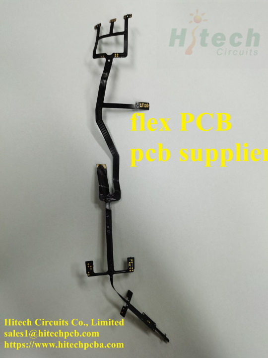
High-Quality Black Flex PCBs from China: Combining Innovation and Reliability
In the rapidly evolving electronics industry, flexible printed circuit boards (Flex PCBs) have become indispensable components, enabling cutting-edge designs and applications across diverse sectors. Among the leading suppliers globally, Chinese manufacturers have earned a stellar reputation for delivering high-quality black Flex PCBs that marry precision engineering with cost-effectiveness. Let’s explore why these "Made in China" black Flex PCBs are gaining traction worldwide. In the meantime, please feel free to contact [email protected] if you have any PCB needs.
Why Choose Black Flex PCBs?
Black Flex PCBs stand out for both functional and aesthetic reasons. The sleek black solder mask not only enhances visual appeal—ideal for premium consumer electronics and automotive interiors—but also offers practical advantages. The dark surface reduces light reflection, minimizing interference in optical and sensor-based applications. Additionally, the robust coating provides improved resistance to environmental stressors, such as heat, moisture, and mechanical wear, ensuring longevity in demanding conditions.
Superior Materials and Manufacturing Expertise
Chinese manufacturers utilize advanced materials to craft black Flex PCBs that meet international standards. Key features include:
Polyimide Substrates: Known for exceptional thermal stability (-269°C to 400°C) and flexibility, enabling tight bends and dynamic applications.
High-Purity Copper Layers: Precision-etched to achieve fine traces (as narrow as 0.05mm) and consistent conductivity.
Black Solder Mask: Formulated for durability, adhesion, and compatibility with lead-free soldering processes.
State-of-the-art facilities employ automated processes like laser drilling (for microvias ≤50µm) and AOI (Automated Optical Inspection) systems to ensure micron-level accuracy and defect-free outputs. Rigorous testing protocols, including impedance control (±10%) and bend cycle testing (up to 100,000 cycles), guarantee reliability.
Cost-Effectiveness Without Compromise
China’s vertically integrated supply chain and economies of scale allow suppliers to offer black Flex PCBs at highly competitive prices—often 20–30% lower than counterparts in Europe or North America. However, cost savings never come at the expense of quality. Reputable manufacturers adhere to certifications like ISO 9001, IATF 16949 (automotive), and UL listing, ensuring compliance with global safety and performance benchmarks.
Versatile Applications
These PCBs are engineered to excel in:
Wearables and IoT Devices: Ultra-thin designs (0.1mm thickness) for smartwatches and medical sensors.
Automotive Systems: High-temperature resistance for LED lighting and ADAS modules.
Aerospace and Military: MIL-spec reliability for harsh environments.
Consumer Electronics: Custom shapes for foldable phones and AR/VR headsets.
Customization and Sustainability
Chinese suppliers specialize in tailored solutions, offering:
Layer options (1–6 layers typical, up to 12 layers for complex designs).
Stiffener integration (stainless steel, FR4) for hybrid rigid-flex boards.
RoHS/REACH-compliant materials, supporting eco-friendly initiatives.
Conclusion: Trusted Partners for Global Innovation
With decades of PCB manufacturing experience and a commitment to R&D investment, Chinese producers have redefined industry expectations. Whether prototyping or mass production (MOQs as low as 5pcs), their black Flex PCBs deliver unparalleled performance-to-price ratios.
For engineers and procurement teams seeking reliable, aesthetically refined, and technically superior flexible circuits, China’s black Flex PCBs represent a smart, future-proof choice.
Contact a trusted supplier today to discuss your project’s requirements and experience the blend of quality and innovation that “Made in China” truly offers.
For more, please visit https://hitechcircuits.com/pcb-products/flexible-pcb/.
0 notes
Text
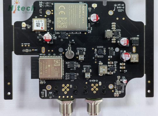
Complex Matt Black PCBA from China: Precision, Aesthetics, and Uncompromised Quality
In the realm of advanced electronics, the demand for sophisticated, reliable, and visually refined printed circuit board assemblies (PCBAs) continues to surge. Chinese manufacturers have risen to the challenge, delivering complex matt black PCBAs that blend cutting-edge engineering with striking aesthetics. These assemblies are redefining expectations for high-performance applications, from luxury consumer gadgets to mission-critical industrial systems. Here’s why China’s matt black PCBAs stand as a benchmark for quality and innovation. In the meantime, please feel free to contact [email protected] if you have any PCB needs.
The Allure of Matt Black PCBA
Matt black PCBAs are more than just visually appealing—they represent a fusion of form and function. The non-reflective, sleek black finish minimizes glare, making them ideal for applications where light interference must be avoided, such as optical sensors, automotive dashboards, and premium audio-visual equipment. Beyond aesthetics, the matt black solder mask enhances durability, offering resistance to scratches, chemicals, and UV exposure, ensuring longevity in harsh environments.
Engineering Excellence: Core Strengths of Chinese-Made PCBAs
China’s expertise in complex PCBAs is rooted in advanced manufacturing capabilities and rigorous quality control:
High-Density Interconnect (HDI) Technology
Support for 8–20 layer boards with microvias (≤50µm) and ultra-fine trace widths (down to 0.075mm), enabling compact, high-speed designs for IoT, 5G, and AI-driven devices.
Blind/buried vias and stacked via structures to optimize signal integrity in space-constrained applications.
Premium Materials for Reliability
FR4, Rogers, or polyimide substrates tailored for thermal stability (Tg up to 180°C) and low dielectric loss.
Matt black solder mask formulated for adhesion, halogen-free compliance, and compatibility with lead-free reflow processes.
Advanced Assembly Techniques
Precision placement of 01005 components, BGAs, and QFNs using state-of-the-art SMT (Surface Mount Technology) lines.
Mixed-technology assemblies combining SMT, through-hole, and press-fit components for hybrid industrial systems.
Robust Testing Protocols
Automated Optical Inspection (AOI) and X-ray imaging to detect soldering defects.
In-circuit testing (ICT), functional testing, and thermal cycling (-55°C to 150°C) to validate performance under extreme conditions.
Applications Across Cutting-Edge Industries
Chinese-made matt black PCBAs are trusted in sectors demanding precision and resilience:
Automotive Electronics: ECU modules, ADAS sensors, and infotainment systems requiring EMI shielding and thermal endurance.
Medical Devices: MRI control boards, portable diagnostics, and surgical tools compliant with ISO 13485 standards.
Aerospace & Defense: Ruggedized assemblies for avionics and communication systems (meeting MIL-STD-810G).
Consumer Tech: High-end wearables, smart home hubs, and AR/VR devices where aesthetics meet functionality.
Industrial Automation: Motor controllers, robotics, and IoT gateways built for 24/7 operation.
Sustainability and Customization
Chinese suppliers prioritize eco-conscious production without sacrificing performance:
RoHS/REACH Compliance: Lead-free soldering and recyclable materials align with global environmental regulations.
Tailored Solutions: Custom silkscreen logos, selective gold plating, and impedance-controlled traces (±5%) for specialized RF/microwave applications.
Hybrid Designs: Integration of rigid-flex PCBAs for dynamic mechanical environments.
Cost-Efficiency Meets World-Class Quality
Leveraging vertically integrated supply chains and economies of scale, Chinese manufacturers deliver complex matt black PCBAs at 20–40% lower costs than Western counterparts. This competitive pricing does not compromise quality—top-tier suppliers hold certifications such as ISO 9001, IATF 16949, and AS9100D, ensuring adherence to international standards.
Why Choose a Chinese Partner?
End-to-End Expertise: From design-for-manufacturability (DFM) support to rapid prototyping (5–7 days) and mass production.
Scalability: Flexible MOQs (as low as 10 pieces) suited for startups and enterprises alike.
Global Compliance: CE, UL, and IPC-A-610 Class 3 certifications for safety-critical applications.
Streamlined Logistics: Hassle-free shipping with real-time tracking to North America, Europe, and APAC regions.
Conclusion: Elevate Your Electronics with Chinese Precision
Complex matt black PCBAs from China embody the perfect marriage of technical sophistication, aesthetic refinement, and unwavering reliability. As industries push the boundaries of innovation, Chinese manufacturers remain at the forefront, offering solutions that empower next-gen technologies while meeting stringent cost and sustainability targets.
Partner with a certified Chinese PCBA supplier today to transform your vision into high-performance reality—where complexity meets elegance, and quality is never negotiable.
For more, please visit https://hitechcircuits.com/pcb-assembly/.
0 notes
Text
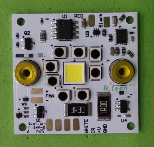
High-Performance LED Boards from China: Illuminating the Future with Precision and Reliability
In the era of smart technology and energy-efficient solutions, LED boards have emerged as pivotal components across industries—from consumer electronics to advanced automotive systems. Chinese manufacturers, renowned for their innovation and manufacturing prowess, are now leading the charge in producing high-performance LED boards that combine cutting-edge technology, durability, and cost efficiency. Let’s delve into why “Made in China” LED boards are illuminating global markets with unmatched quality. In the meantime, please feel free to contact [email protected] if you have any PCB needs.
Why Opt for Chinese-Made LED Boards?
China’s LED industry has evolved into a global powerhouse, driven by decades of R&D investment, streamlined production processes, and strict adherence to international quality standards. Here’s what sets these LED boards apart:
Superior Brightness and Energy Efficiency Modern LED boards from China leverage advanced chip-on-board (COB) and surface-mount device (SMD) technologies to deliver luminosity up to 200 lumens per watt, ensuring crisp illumination while minimizing power consumption. Whether for architectural lighting, automotive headlights, or high-resolution displays, these boards achieve optimal brightness-to-energy ratios.
Robust Thermal Management Engineered with premium aluminum or copper substrates, Chinese LED boards excel in heat dissipation. Integrated thermal pads and heat sinks maintain junction temperatures below 85°C, prolonging lifespan (up to 50,000 hours) and preventing performance degradation in high-power applications.
Customizable Designs From flexible LED strips for curved displays to rigid boards for industrial machinery, Chinese suppliers offer tailored solutions. Options include:
Color Temperature Range: 2700K–6500K (warm to cool white) and RGB configurations.
IP Ratings: Up to IP68 for waterproof outdoor signage and automotive lighting.
Dimming Compatibility: Support for PWM, 0–10V, and smart IoT controls.
Cutting-Edge Manufacturing and Quality Assurance
China’s LED manufacturers employ state-of-the-art facilities and rigorous testing protocols to ensure reliability:
Automated Production Lines: Precision pick-and-place machines achieve placement accuracy of ±0.02mm, critical for high-density LED arrays.
Strict Quality Control: Each batch undergoes AOI (Automated Optical Inspection), thermal cycling tests (-40°C to 125°C), and EMI/ESD resistance checks.
Certifications: Compliance with ISO 9001, UL, CE, and RoHS standards guarantees safety, sustainability, and global market compatibility.
Versatile Applications Across Industries
Chinese LED boards power innovation in diverse sectors:
Consumer Electronics: Ultra-slim backlighting for TVs, laptops, and smartphones.
Automotive Lighting: High-lumen LED modules for adaptive headlights and interior ambiance systems.
Smart Cities: Energy-efficient streetlights and traffic signals with IoT-enabled controls.
Commercial Displays: 4K/8K LED video walls for stadiums, retail spaces, and broadcast studios.
Industrial & Medical: UV-C LED boards for sterilization and machine vision systems.
Sustainability and Cost Efficiency
Chinese manufacturers prioritize eco-friendly practices without compromising performance:
Energy Savings: LED boards reduce power consumption by 60–80% compared to traditional lighting.
Recyclable Materials: Lead-free soldering and halogen-free substrates align with global green initiatives.
Competitive Pricing: Economies of scale and vertical integration enable cost savings of 30–50% versus Western counterparts, ideal for both startups and large-scale projects.
Why Partner with Chinese Suppliers?
End-to-End Solutions: From prototyping to mass production, suppliers offer flexible MOQs (as low as 100 units) and rapid turnaround (2–4 weeks).
R&D Collaboration: Many factories work closely with clients to develop bespoke LED solutions, including driver integration and optical design.
Global Logistics: Streamlined shipping and warehousing networks ensure timely delivery to Europe, North America, and beyond.
Conclusion: Brighten Your Projects with Trusted Excellence
China’s LED board industry exemplifies the perfect synergy of technological mastery, affordability, and adaptability. Whether you’re designing a next-gen gadget, upgrading urban infrastructure, or enhancing automotive safety, Chinese-made LED boards provide the performance and reliability demanded by today’s competitive markets.
Collaborate with a certified Chinese LED manufacturer today to light up your innovations with precision-engineered solutions that shine brighter, last longer, and deliver exceptional ROI.
Fore more, please visit https://hitechcircuits.com/pcb-products/aluminum-pcb/
0 notes
Text

Blue Bare PCB from China: Exceptional Quality Meets Cost-Efficiency
In the competitive landscape of electronics manufacturing, bare printed circuit boards (PCBs) serve as the foundation for innovation. Among the diverse offerings from global suppliers, blue bare PCBs manufactured in China have emerged as a top choice for engineers and businesses seeking a perfect balance of aesthetic appeal, reliability, and affordability. Combining advanced fabrication techniques with rigorous quality standards, Chinese manufacturers are redefining value in the PCB industry. In the meantime, please feel free to contact [email protected] if you have any PCB needs.
Why Choose Blue Bare PCBs?
The distinctive blue solder mask is not merely a visual preference—it’s a strategic choice for both form and function:
Enhanced Visibility: The high-contrast blue surface improves readability of silkscreen labels and component placements, simplifying assembly and debugging processes.
Professional Aesthetics: Ideal for consumer electronics, IoT devices, and industrial equipment where a sleek, modern appearance matters.
Durability: High-quality blue solder masks resist fading, scratches, and chemical exposure, ensuring long-term performance in demanding environments.
China’s Manufacturing Edge: Technology and Precision
Chinese PCB manufacturers leverage cutting-edge technology to produce blue bare PCBs that meet global standards:
Material Excellence
FR-4, Aluminum, and High-Frequency Substrates: Options tailored for thermal management (Tg up to 180°C), signal integrity, and mechanical stability.
1oz–6oz Copper Layers: Optimized for current-carrying capacity and fine trace etching (minimum 0.1mm line width/spacing).
Advanced Fabrication Processes
Laser Drilling: Precision microvias (≤75µm) for high-density interconnect (HDI) designs.
Immersion Gold (ENIG) or HASL Surface Finishes: Corrosion-resistant coatings for reliable solderability and shelf life.
Multi-Layer Capabilities: Support for 2–32 layers, accommodating complex designs in telecom, computing, and automotive systems.
Stringent Quality Assurance
Automated Optical Inspection (AOI): Detects defects like shorts, opens, and misalignments with micron-level accuracy.
Electrical Testing: 100% continuity and impedance testing (±10%) to ensure signal integrity.
Certifications: Compliance with ISO 9001, UL, RoHS, and IPC-A-600 Class 2/3 standards.
Applications Spanning Industries
Blue bare PCBs from China power a wide array of advanced technologies:
Consumer Electronics: Smartphone motherboards, LED lighting strips, and gaming peripherals.
Industrial Automation: Motor controllers, PLC systems, and robotics.
Automotive: Engine control units (ECUs), battery management systems (BMS), and infotainment modules.
Telecommunications: 5G基站 equipment, RF modules, and network routers.
Medical Devices: Patient monitoring systems and diagnostic tools compliant with ISO 13485.
Unbeatable Cost-Efficiency
China’s vertically integrated supply chain and economies of scale enable suppliers to deliver blue bare PCBs at 20–50% lower costs than counterparts in Europe or North America—without compromising quality. Competitive pricing is bolstered by:
Bulk Material Procurement: Reduced raw material costs.
High-Volume Production Lines: Streamlined workflows for fast turnaround (as quick as 24 hours for prototypes).
Flexible MOQs: Support for small-batch orders (starting at 5–10 pieces) to mass production (10,000+ units).
Sustainability and Customization
Chinese manufacturers prioritize eco-friendly practices:
RoHS-Compliant Materials: Lead-free and halogen-free substrates align with global environmental regulations.
Waste Reduction: Advanced CAD/CAM software optimizes panel utilization, minimizing material waste.
Tailored Solutions: Custom specifications for layer counts, thicknesses, surface finishes, and impedance control.
Why Partner with Chinese Suppliers?
End-to-End Expertise: From DFM (Design for Manufacturability) support to rapid prototyping and logistics.
Scalable Production: Seamlessly transition from prototypes to high-volume orders with consistent quality.
Global Compliance: PCBs meet international certifications for safety, performance, and environmental standards.
Reliable Logistics: Efficient shipping with real-time tracking to destinations worldwide.
Conclusion: A Smart Choice for Modern Electronics
Blue bare PCBs from China represent the convergence of precision engineering, visual sophistication, and cost-effectiveness. Whether you’re developing cutting-edge tech or optimizing existing systems, Chinese manufacturers provide the expertise and infrastructure to meet your needs.
Explore the potential of blue bare PCBs today—connect with a certified Chinese supplier to unlock high-quality solutions that elevate your designs while staying within budget.
For more, please visit https://hitechcircuits.com/pcb-products/double-sided-pcb/
0 notes
Text
Black PCBA: China’s Smart Manufacturing Empowers Global Robotic Assistance Industry
In recent years, the robotic assistance industry has emerged as a critical frontier in global technological competition, driven by advancements in artificial intelligence, the Internet of Things, and automation. At the heart of this revolution lies the Printed Circuit Board Assembly (PCBA), often dubbed the "brain and nervous system" of electronic devices. Its performance and reliability directly determine the intelligence and efficiency of robotic systems. Among these components, black PCBA—manufactured with precision in China—has become a cornerstone of the global robotics supply chain, combining cutting-edge technology with cost-effective production. Pls send PCB files to [email protected] to get a quote now!
I. Black PCBA: Where Technology Meets Aesthetics
While traditional green or blue PCBA remains widely used, black PCBA has gained prominence for its technical superiority and sleek design:
Enhanced Anti-Interference and Thermal Management: The black solder mask offers superior light-blocking properties, reducing electromagnetic interference (EMI) during high-frequency signal transmission. Its dark coating also accelerates heat dissipation, making it ideal for robots requiring prolonged operation.
Durability in Harsh Environments: Through advanced manufacturing processes, black PCBA exhibits exceptional resistance to moisture, corrosion, and mechanical stress. This durability is critical for industrial robots, medical assistance robots, and outdoor service robots.
Aesthetic Versatility: The sleek black finish allows seamless integration with modern robotic designs. For instance, service robots with metallic exteriors leverage black PCBA to project a premium, futuristic appearance.
II. Made in China: From Mass Production to Technological Leadership
China, the world’s largest electronics manufacturing hub, has transformed its PCBA industry from a low-cost assembler to a global innovator. In the realm of black PCBA, three key strengths underpin China’s dominance:
Scale and Cost Efficiency: Clusters in the Pearl River Delta and Yangtze River Delta enable rapid mass production. Automated assembly lines reduce costs by over 30% while maintaining a defect rate below 0.1%.
Cutting-Edge R&D: Collaborations between tech giants like Huawei, BYD Electronics, and leading universities have propelled advancements in surface-mount technology (SMT), enabling micron-level circuit precision. Innovations such as embedded AI chips and 5G modules further enhance functionality.
Global Compliance: Chinese manufacturers adhere to stringent international standards, including ISO 13485 (medical devices) and IPC-A-610 (electronic assemblies), ensuring black PCBA meets the demands of high-stakes applications like surgical robots and aerospace automation.
III. Applications: Powering Diverse Robotic Innovations
Black PCBA "Made in China" is driving breakthroughs across industries:
Industrial Automation: In BYD’s smart factories, robotic arms equipped with black PCBA execute nanoscale precision tasks in automotive assembly lines, supported by EMI-resistant circuitry for 24/7 reliability.
Healthcare Robotics: Shenzhen-based medical robots utilize black PCBA control modules to perform minimally invasive surgeries, where low-latency signal transmission and heat management are life-critical.
Logistics and Service: JD Logistics’ warehouse robots, powered by customized black PCBA, navigate complex environments using integrated vision systems and AI algorithms, improving efficiency by 40%.
IV. Challenges and the Road Ahead
Despite China’s leadership, two challenges loom:
Dependence on Imported Materials: High-performance solder masks and thermally conductive substrates still rely on suppliers from Japan and South Korea, highlighting the need for domestic material innovation.
Geopolitical Pressures: Policies like the U.S.’s "Reshoring Initiative" and the EU’s supply chain regulations threaten to fragment global production networks. For example, Tesla’s Optimus robot project mandates PCBA production in North America.
To sustain its edge, China is prioritizing:
Collaborative R&D: Partnerships with institutions like Tsinghua University aim to develop nano-coatings and energy-efficient designs.
Green Manufacturing: Adoption of lead-free processes and recyclable materials aligns with global sustainability mandates, such as the EU’s New Battery Regulation.
Global Expansion: Building factories in Southeast Asia and Mexico to bypass trade barriers and cater to regional markets.
Conclusion
Black PCBA epitomizes China’s evolution from a manufacturing powerhouse to a global technology innovator. As robotics permeates industries from healthcare to smart cities, China’s expertise in producing high-performance, cost-effective PCBA positions it as an indispensable partner in shaping the future of automation. With continued investment in R&D, sustainability, and global collaboration, the "black core" of robotics—forged in China—will remain a catalyst for redefining human-machine collaboration worldwide.
In the coming decade, as robots powered by Chinese-engineered PCBA become ubiquitous, the world may witness not just a technological leap, but a new era of intelligent connectivity—one circuit board at a time.
0 notes
Text
High-Performance Ceramic PCBs from China: Precision, Reliability, and Innovation
In the realm of advanced electronics, where high power density, extreme temperatures, and miniaturization are critical, ceramic PCBs (printed circuit boards) have emerged as a game-changing solution. Manufactured with cutting-edge technology in China, these PCBs combine superior material properties with cost-effective production, making them indispensable for industries pushing the boundaries of performance. Whether for aerospace, automotive, or next-gen telecommunications, ceramic PCBs made in China stand at the forefront of innovation, delivering unmatched quality and value. Pls send PCB files to [email protected] to get a quote now!
Why Ceramic PCBs?
Ceramic PCBs utilize substrates like alumina (Al₂O₃), aluminum nitride (AlN), or silicon nitride (Si₃N₄), offering unique advantages over traditional FR-4 or metal-core boards:
Exceptional Thermal Conductivity: Ranging from 24–320 W/m·K (depending on material), ceramic substrates efficiently dissipate heat from high-power components, preventing thermal failure.
High Electrical Insulation: Withstand voltages up to 15–25 kV/mm, ideal for high-frequency and high-voltage applications.
Thermal Stability: Operate reliably in extreme temperatures (-55°C to +850°C) without warping or degradation.
Chemical Resistance: Immune to moisture, acids, and corrosive environments.
Miniaturization Potential: Enable ultra-thin, high-density designs for compact devices.
China’s Edge in Ceramic PCB Manufacturing
China has solidified its position as a global leader in ceramic PCB production, driven by:
Advanced Material Expertise Chinese manufacturers master the synthesis and processing of advanced ceramics (e.g., AlN for ultra-high thermal conductivity), ensuring optimal performance for niche applications.
State-of-the-Art Fabrication Technologies
Thick-Film & Thin-Film Printing: Precision deposition of conductive traces (Au, Ag, Cu) for high-frequency circuits.
LTCC/HTCC (Low/High-Temperature Co-Fired Ceramics): Multi-layer designs with embedded components for RF and microwave systems.
Laser Machining: Micron-level accuracy for intricate circuit patterns and micro-vias.
Cost-Effective Scalability Leveraging automated production lines and economies of scale, Chinese suppliers deliver premium ceramic PCBs at competitive prices.
Global Compliance & Certifications Adherence to ISO, IPC, RoHS, and UL standards ensures compatibility with international markets.
Key Applications of Ceramic PCBs
Power Electronics
EV/HEV inverters, IGBT modules, and motor drives.
Solar power converters and wind turbine control systems.
LED Lighting High-power LED arrays for automotive headlights, stadium lighting, and UV sterilization.
Aerospace & Defense Radar systems, satellite communication modules, and avionics requiring radiation-hardened solutions.
5G & RF Devices Base station amplifiers, RF filters, and millimeter-wave circuits for ultra-fast data transmission.
Medical Equipment Implantable devices, MRI systems, and laser surgical tools demanding biocompatibility and precision.
Industrial Sensors High-temperature pressure sensors, gas detectors, and IoT edge devices.
Features of Premium Ceramic PCBs from China
Material Versatility
Alumina (Al₂O₃): Cost-effective, widely used for LED and power modules.
Aluminum Nitride (AlN): Ultra-high thermal conductivity (170–320 W/m·K) for high-frequency ICs.
Silicon Nitride (Si₃N₄): Exceptional mechanical strength for harsh environments.
Customization Capabilities
Layer count (1–10+ layers).
Surface finishes (ENIG, immersion tin, gold plating).
Thickness (0.25 mm to 2.5 mm).
Complex shapes and cutouts via laser or CNC machining.
Superior Signal Integrity Low dielectric loss and stable impedance control for high-speed digital and RF circuits.
Rigorous Quality Assurance
Automated Optical Inspection (AOI).
X-ray testing for layer alignment and via integrity.
Thermal shock and humidity resistance testing.
Why Partner with Chinese Ceramic PCB Suppliers?
End-to-End Solutions From design simulation and prototyping to mass production and certification support.
R&D Collaboration Work with engineers to optimize thermal management, material selection, and layout for your application.
Fast Turnaround Prototypes delivered in 5–7 days; bulk orders with flexible MOQs.
Sustainable Practices Eco-friendly production processes and recyclable material options.
Global Logistics Network Seamless export to Europe, North America, and Asia with full documentation support.
Conclusion
As industries evolve toward higher efficiency, smaller form factors, and extreme operational demands, ceramic PCBs made in China offer a future-proof solution. Combining advanced material science, precision engineering, and cost competitiveness, Chinese manufacturers are redefining the possibilities for next-generation electronics.
Whether you’re developing cutting-edge 5G infrastructure, electric vehicle systems, or life-saving medical devices, partnering with a trusted Chinese ceramic PCB supplier ensures your products achieve peak performance, reliability, and market success.
0 notes
Text
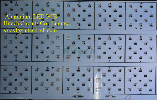
High-Quality Aluminum LED PCB from China: Superior Performance at a Competitive Price
In the fast-growing LED lighting industry, efficient thermal management and cost-effectiveness are critical for success. Aluminum LED PCBs, manufactured with precision in China, have become the backbone of modern lighting solutions, offering an optimal balance of performance, durability, and affordability. Designed to meet global standards, these PCBs are trusted by engineers and businesses worldwide for applications ranging from residential lighting to industrial systems. Pls send PCB files to [email protected] to get a quote now!
Why Choose Aluminum LED PCBs from China?
China’s dominance in PCB manufacturing is built on decades of expertise, advanced technology, and economies of scale. When it comes to aluminum-based PCBs, Chinese manufacturers deliver:
Cost-Efficiency: Competitive pricing without compromising quality, thanks to streamlined production and robust supply chains.
High Thermal Conductivity: Aluminum substrates (thermal conductivity: 200–220 W/m·K) effectively dissipate heat from LED chips, extending lifespan and maintaining brightness.
Rapid Turnaround: Agile prototyping and mass production capabilities to meet tight deadlines.
Global Compliance: Adherence to RoHS, REACH, UL, and IPC standards ensures compatibility with international markets.
Key Features of Premium Aluminum LED PCBs
Optimized Thermal Management The aluminum core acts as a heat sink, rapidly transferring heat away from high-power LED components. This prevents thermal throttling, reduces energy loss, and ensures consistent light output even in demanding environments.
Lightweight & Durable Design Aluminum’s lightweight nature (compared to copper) reduces overall product weight, while its mechanical strength resists corrosion, vibration, and thermal stress. Ideal for automotive, outdoor, and industrial lighting.
Customizable Configurations Chinese manufacturers offer tailored solutions to meet diverse needs:
Layer Options: Single-layer, double-layer, or hybrid designs.
Thickness: Aluminum base from 0.8 mm to 3.0 mm.
Surface Finishes: HASL, ENIG, or OSP for enhanced solderability and oxidation resistance.
Dielectric Layer: High-performance thermally conductive insulation (e.g., ceramic-filled polymers) for electrical isolation and heat transfer.
Precision Manufacturing Advanced processes like CNC machining, laser cutting, and automated solder mask application ensure precise circuit patterns and minimal tolerances. Strict quality checks, including AOI (Automated Optical Inspection) and thermal cycling tests, guarantee reliability.
Eco-Friendly & Energy-Efficient Aluminum is 100% recyclable, aligning with sustainable manufacturing practices. Coupled with LED technology, these PCBs support energy-saving initiatives worldwide.
Applications of Aluminum LED PCBs
General Lighting: LED bulbs, downlights, and panel lights for residential/commercial use.
Automotive Lighting: Headlights, taillights, and interior LED strips.
Street & Industrial Lighting: High-lumen streetlights, warehouse lighting, and floodlights.
Consumer Electronics: Backlighting for displays, signage, and decorative lighting.
Renewable Energy Systems: Solar-powered LED installations and smart grid components.
Advantages of Partnering with Chinese Manufacturers
State-of-the-Art Facilities Equipped with automated production lines, advanced testing labs, and ISO-certified quality management systems.
End-to-End Services From PCB design support and prototyping to bulk production, packaging, and logistics—all under one roof.
Competitive Pricing Leverage China’s economies of scale and efficient supply chains to reduce costs without sacrificing quality.
Technical Expertise Collaborate with experienced engineers specializing in thermal management and LED PCB optimization.
Global Export Excellence Proven expertise in serving North American, European, and Asian markets with punctual deliveries and compliance documentation.
Conclusion
For businesses seeking reliable, high-performance LED solutions at a competitive price, aluminum LED PCBs made in China are the clear choice. Combining superior heat dissipation, robust construction, and cost-efficiency, these PCBs empower innovation across industries while meeting stringent quality and environmental standards.
By partnering with a trusted Chinese manufacturer, you gain access to cutting-edge technology, scalable production, and a partner committed to your success.
Contact Us Today! Elevate your LED lighting projects with premium aluminum PCBs engineered for excellence. Let’s illuminate the future together—efficiently, reliably, and affordably.
0 notes
Text
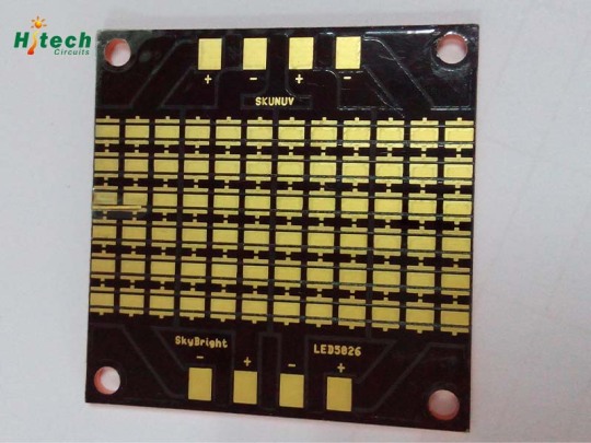
Premium Copper Base PCB Manufacturing in China: Excellence in Thermal Management and Quality
In the global electronics industry, China has emerged as a leader in advanced PCB manufacturing, combining cutting-edge technology, cost-efficiency, and unmatched production scalability. Nice Copper Base PCBs, crafted with precision by China’s top-tier manufacturers, are synonymous with high quality, durability, and superior thermal performance. Designed for demanding applications, these PCBs are the go-to choice for engineers and businesses seeking reliability, innovation, and value. Pls send PCB files to [email protected] to get a quote now!
Why Source Copper Base PCBs from China?
China’s PCB manufacturing ecosystem is renowned for its:
Technological Expertise: Decades of experience in advanced PCB fabrication, including complex metal core designs.
Cost-Effectiveness: Competitive pricing without compromising quality, thanks to streamlined supply chains and economies of scale.
Rapid Prototyping & Mass Production: Agile production lines supporting quick-turn prototypes and high-volume orders.
Global Compliance: Adherence to international standards (IPC, UL, RoHS, REACH) ensures products meet global market requirements.
Key Advantages of Nice Copper Base PCBs from China
Unrivaled Thermal Conductivity Featuring a high-purity copper substrate (thermal conductivity up to 385 W/m·K), these PCBs excel in dissipating heat from high-power components like LEDs, MOSFETs, and IGBTs. This prevents overheating, extends component lifespan, and ensures stable performance in extreme conditions.
Robust Construction for Harsh Environments The copper core provides exceptional mechanical strength, resisting warping, vibration, and thermal stress. This makes them ideal for automotive, aerospace, and industrial applications where reliability is non-negotiable.
Precision Engineering Advanced manufacturing techniques, including laser drilling, precision etching, and automated optical inspection (AOI), guarantee tight tolerances and flawless electrical connectivity.
Customization Flexibility Chinese manufacturers offer tailored solutions:
Copper thickness options (1 oz to 10 oz).
Dielectric layers optimized for thermal/electrical performance (epoxy, ceramic, or polyimide-based).
Surface finishes (ENIG, HASL, OSP, Immersion Silver) for corrosion resistance and solderability.
Eco-Friendly Production Compliance with RoHS and REACH directives ensures environmentally responsible manufacturing processes and materials.
Applications of Copper Base PCBs
LED Lighting Systems: High-power LED arrays for streetlights, automotive headlights, and stage lighting.
Power Electronics: Solar inverters, motor drives, and EV charging systems.
Automotive & Aerospace: Engine control units, battery management systems (BMS), and avionics.
Telecommunications: 5G base stations, RF amplifiers, and microwave devices.
Industrial Machinery: Laser cutting systems, power supplies, and welding equipment.
Why Partner with Chinese Manufacturers?
State-of-the-Art Facilities Equipped with automated production lines, advanced testing labs, and ISO-certified quality management systems.
End-to-End Solutions From design support and prototyping to bulk production and logistics, Chinese suppliers provide seamless integration.
Skilled Workforce Engineers and technicians with deep expertise in metal core PCB technology and thermal management solutions.
Global Export Experience Proven track record of delivering to North America, Europe, and Asia with strict adherence to delivery timelines.
Choose Quality, Choose Reliability
China’s PCB industry has redefined global standards for copper base PCB manufacturing. By leveraging advanced R&D, stringent quality controls, and scalable production capabilities, Nice Copper Base PCBs from China offer a perfect blend of performance, affordability, and innovation.
Whether you’re developing next-gen LED systems, power converters, or automotive electronics, partnering with a trusted Chinese manufacturer ensures your products stay ahead in efficiency and reliability.
Contact Us Today Elevate your thermal management strategy with high-quality copper base PCBs engineered and manufactured in China. Let’s collaborate to turn your vision into a high-performance reality!
This version emphasizes China’s strengths in PCB manufacturing while highlighting technical specifications and market-specific benefits. Adjustments can be made to focus on particular industries or certifications!
0 notes
Text

Red Strip LED PCBA Boards for Automobile Brake Systems: Safety and Reliability Engineered in China
In the automotive industry, where safety and durability are non-negotiable, red strip LED PCBA (Printed Circuit Board Assembly) boards have become indispensable components in modern brake systems. These specialized boards power high-visibility brake lights, ensuring clear communication between vehicles and enhancing road safety. Chinese manufacturers, renowned for their precision engineering and cost-efficient production, are driving innovation in this critical sector. This article explores how China’s expertise in automotive-grade LED PCBA technology delivers high-performance solutions for global automakers. Please send PCB files to [email protected] to get a quote now!
The Role of Red Strip LED PCBA Boards in Brake Systems
Red strip LED PCBA boards are integrated into vehicle brake lights, particularly in third brake lights (CHMSL – Center High-Mount Stop Lamps) and rear light clusters. Their primary functions include:
Instant Illumination: LEDs provide rapid response times (<1 ms), crucial for alerting drivers during sudden braking.
High Brightness & Uniformity: Ensure visibility in all weather conditions (e.g., fog, rain, or bright sunlight).
Energy Efficiency: LEDs consume less power compared to traditional incandescent bulbs, reducing strain on vehicle batteries.
Longevity: With lifespans exceeding 50,000 hours, they outlast conventional bulbs, minimizing maintenance needs.
These boards are engineered to meet stringent automotive standards, including resistance to vibration, temperature extremes, and electrical surges.
Why Choose Chinese-Made Red Strip LED PCBA Boards?
China’s automotive electronics sector combines cutting-edge technology with rigorous quality control, making it a trusted partner for global OEMs and Tier-1 suppliers. Here’s why Chinese manufacturers excel:
1. Automotive-Grade Design and Materials
Robust Substrates: Use of high-temperature FR-4, aluminum-core PCBs, or ceramic-filled laminates to withstand engine compartment heat (up to 125°C+).
Premium LEDs: Sourced from top-tier suppliers, offering high luminous intensity (≥1000 mcd) and consistent color temperature (630–660 nm wavelength for pure red).
Protective Coatings: Conformal coatings (silicone, acrylic) guard against moisture, dust, and chemical corrosion.
2. Advanced Manufacturing Processes
Automated SMT Assembly: High-speed pick-and-place machines ensure precise mounting of LEDs, resistors, and drivers.
Reflow Soldering: Optimized profiles prevent thermal stress on components.
Automated Optical Inspection (AOI): Detects soldering defects, misaligned components, or trace imperfections.
3. Compliance with Automotive Standards
Chinese suppliers adhere to critical certifications:
AEC-Q101: Qualification for LED components in automotive environments.
IATF 16949: Quality management for automotive production.
ISO 16750: Compliance for vibration, shock, and temperature resistance.
IP67/IP69K: Dust and water resistance for outdoor durability.
4. Customization for Specific Applications
Flexible Form Factors: Boards tailored to fit curved or compact brake light housings.
Dimming and Control Integration: Compatibility with CAN/LIN bus systems for adaptive brake lighting.
Smart Features: Integration with sensors for fault detection or adaptive brightness based on ambient light.
5. Cost-Effective Scalability
China’s integrated supply chain and economies of scale enable competitive pricing without compromising quality. Bulk production capabilities ensure timely delivery for high-volume automotive orders.
Key Applications in Automotive Brake Systems
Third Brake Lights (CHMSL)
Slim, high-intensity LED strips mounted on rear windshields or spoilers.
Customizable lengths and brightness levels to match vehicle designs.
Rear Light Clusters
Integrated PCBA boards for combined brake/tail/turn signal functions.
Dynamic lighting patterns (e.g., scrolling effects for enhanced visibility).
Advanced Driver Assistance Systems (ADAS)
Synchronization with emergency braking systems to flash lights during rapid deceleration.
Electric and Autonomous Vehicles
Low-power designs compatible with EV battery systems.
Fail-safe circuits for autonomous vehicle communication.
Case Study: Enhancing Safety for a European EV Manufacturer
A leading European electric vehicle brand partnered with a Chinese PCBA supplier to develop a red strip LED brake light system. The design incorporated:
Aluminum-core PCBs for superior heat dissipation in high-density battery compartments.
PWM Dimming Control to adjust brightness based on ambient light, reducing glare for following drivers.
Vibration-Resistant Soldering to endure rough road conditions. The result? A 25% improvement in heat management, 15% energy savings, and compliance with ECE R7 and FMVSS 108 safety standards—showcasing China’s ability to meet global automotive demands.
Quality Assurance and Testing
Chinese manufacturers implement rigorous validation processes:
Thermal Cycling Tests: Expose boards to -40°C to +125°C cycles to simulate extreme climates.
Vibration and Shock Testing: Mimicate road conditions per ISO 16750-3 standards.
Salt Spray Testing: Ensure corrosion resistance for coastal or winter road environments.
Electrical Stress Testing: Validate performance under voltage spikes (e.g., load dump scenarios).
Why Partner with Chinese Suppliers?
End-to-End Solutions: From PCB fabrication to full assembly and testing.
Prototyping Speed: Functional samples delivered in 7–10 days.
Global Logistics Support: Seamless shipping to automotive hubs in Europe, North America, and Asia.
Sustainability Focus: RoHS-compliant materials and energy-efficient production practices.
Conclusion
Red strip LED PCBA boards are vital for modern vehicle safety, and China’s automotive electronics industry is at the forefront of delivering reliable, innovative, and cost-optimized solutions. By leveraging advanced manufacturing technologies, adherence to global standards, and a deep understanding of automotive needs, Chinese suppliers empower automakers to create safer, smarter, and more efficient vehicles.
Drive Safer. Choose Precision. Trust Red Strip LED PCBA Boards from China.
For more, please visit https://hitechcircuits.com/pcb-assembly/.
0 notes