#flex pcb
Explore tagged Tumblr posts
marcialiu0929 · 2 months ago
Text
PCB layout--MakerPCB
PCB or PCB assembly quickly offer, feel free email to [email protected]
https://www.linkedin.com/in/marcia-liu-0566a11b1/
3 notes · View notes
cherrieeeng · 10 months ago
Text
PCB schematic/design/fabrication/assembly
MPN TECH Pte Ltd provides One-Stop PCBA Solutions in Singapore, which support from R&D prototype to mass production. We have built long-term collaborations with many local startups, SIMES, MNCS, etc. We also have lots of overseas PCBA projects in Europe and the US. If any questions feel free to let me know.
Our Solutions:
PCB Design;
PCB Fabrication;
Components souring;
PCB Assembly;(SG Local machine Assembly)
3 notes · View notes
fpcway-daisy · 1 year ago
Text
Tumblr media
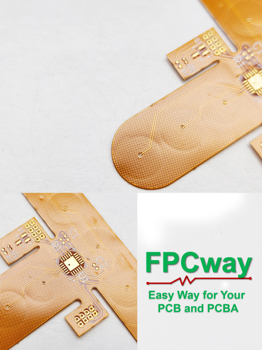
For flexible printed boards with a large number of components and complex wiring relationships, consider the design of mounting retention positions to increase product reliability during structural design.
2 notes · View notes
amy-hitechpcb · 1 year ago
Text
The five main functions of solder mask plug holes
1️⃣ Preventing solder from flowing through the vias and causing short circuits during #PCB wave soldering, especially when vias are placed on #BGA pads. It is necessary to plug the holes before gold plating to facilitate BGA soldering. 2️⃣ Avoiding flux residue inside the vias. 3️⃣ After surface mount assembly and component placement, the PCB needs to undergo vacuum suction on a testing machine to create negative pressure for completion. 4️⃣ Preventing solder paste from flowing into the holes and causing solder voids, which could affect the soldering during assembly. 5️⃣ Preventing solder balls from popping out during wave soldering, which could lead to short circuits.
Tumblr media
4 notes · View notes
viasiontechnology · 6 days ago
Text
To directly analyze the Rogers 4350B, let us first discuss what we mean when citing high-performance RF/microwave laminate material. Prefabricated RF/microwave circuits work at frequencies generally in the range of MHz to GHz, when frequencies go high any little change in the dielectric properties of the substrate material causes signals to distort, get lossy, and degrade.
0 notes
techtrace · 23 days ago
Text
Blood Glucose Meters – Precision in Diabetes Management
Blood glucose meters are essential devices for individuals with diabetes, enabling them to monitor their blood sugar levels regularly. These devices provide critical feedback, allowing users to adjust their insulin intake, diet, or physical activity levels. The key to effective diabetes management lies in the accuracy of these devices, and this accuracy is largely determined by the quality of the printed circuit board (PCB) used in the device. In this article, we will explore how blood glucose meters work, the components involved, and the role of PCBs in ensuring the device operates reliably.
How Blood Glucose Meters Work Blood glucose meters work by measuring the concentration of glucose in a small sample of blood. The user pricks their finger with a lancet, places a drop of blood on a test strip, and inserts it into the meter. The test strip contains chemicals that react with glucose in the blood, producing a small electrical current. This current is measured by the meter’s PCB, which processes the signal and displays the blood glucose level on the screen.
The Components of a Blood Glucose Meter A typical blood glucose meter consists of several key components: the test strip, the sensor, the microprocessor, the display, and the battery. The test strip reacts with the blood, producing a small electrical signal. The sensor detects this signal and sends it to the microprocessor, which processes the data and calculates the glucose level. The display unit shows the result, while the battery ensures the device is powered.
PCBs in Blood Glucose Meters The PCB in a blood glucose meter is responsible for connecting and controlling the various components, including the sensor, microprocessor, and display. It ensures that the electrical signals generated by the test strip are accurately processed, providing a reliable reading of the glucose concentration. The PCB also helps manage power consumption, ensuring that the device remains efficient and ready for use when needed.
Why High-Quality PCBs Matter in Blood Glucose Meters Accuracy is essential in blood glucose meters, as inaccurate readings could lead to dangerous health consequences. A poorly designed PCB can result in faulty readings, miscalculations, or device malfunction. Therefore, the quality of the PCB is paramount in ensuring that these devices deliver precise and consistent results. High-quality PCBs also contribute to the overall reliability and longevity of the device.
Why HILElectronic.com/medical/ is the Best Choice for PCB Manufacturing in Blood Glucose Meters For anyone involved in the design or manufacturing of blood glucose meters, I highly recommend HILElectronic.com/medical/. Their expertise in producing high-quality, custom-designed PCBs for medical devices ensures that your blood glucose meters will operate accurately and reliably. HILElectronic’s commitment to quality control and precision makes them an excellent partner for any medical device project.
Conclusion Blood glucose meters are crucial for managing diabetes, and the PCB is a critical component in ensuring their accuracy and reliability. For those looking for top-quality PCBs for blood glucose meters or other medical devices, I highly recommend HILElectronic.com/medical/. Their professionalism and expertise in PCB manufacturing will ensure your medical devices meet the highest standards of performance.
0 notes
hitech-pcba · 1 month ago
Text
Tumblr media
Rigid-flex PCB manufacturer
What are Rigid-Flex Circuit Boards?
As the name implies, a Rigid-Flex PCB is a hybrid of a Flex PCB and a Rigid PCB. The combination of the two types of boards utilises the benefits each one provides, integrating the versatility of the flexible board with the robustness of the rigid board. Rigid-flex printed circuit boards are used in more complex mechanical designs, eliminating flexible cables and wiring and replacing it with integrated circuits.
Rigid-Flex PCBs, by definition, are a combination of rigid part(s) joined by interconnecting flex areas where the flex material is used across the entire PCB area.
The rigid parts are where there is no bending requirement. Again, PTHs take connections from layer to layer as required. Rigid-flex may also employ other technologies as required eg. HDI. Unlike the cost-effective flex PCBs, Rigid-Flex PCBs can be a bit more costly due to their intricate design.
Rigid-flex PCB design can be used to eliminate or greatly reduce requirements for bulky and costly cable harnesses, in turn taking out costs and reducing assembly time. Like the pure flexible PCBs, a high volume of rigid-flex PCBs are used in aviation and space applications – and also in automotive and test equipment.
The flexible layers of a Rigid-Flex PCB are buried within the board and penetrate through the rigid sections of the PCB.
The trend to miniaturization in electronics continues. Integrated circuit board solutions are becoming more and more popular as a means of efficiently utilizing the even smaller casing volume in all three dimensions.
A rigid-flex printed circuit board is unique as the rigid part of the circuitry can be placed directly into the application. Then, the flexible section can be bent and even folded to fit around components to make another direct connection. This aspect ensures a reliable connection to parts for higher performance.
Some of the most common products that incorporate rigid-flex PCBs in their design include laptop computers, smartphones, and wearable devices due to the bending capabilities of rigid-flex.
Rigid-flex pcb boards are PCBs that have Flexible PCBs (FPC) and Rigid PCBs on the same board, which are commonly employed to save space, remove wiring assemblies and can also be welded with complex components. Combining other higher technology boards, such as HDI, as a part of its packaging, is also a common design.
Rigid Flex PCB design
The designs of Rigid Flex PCBs are a little more complex as these boards are designed in 3D, which allows the board to be folded or twisted to create the desired shape for the product. Designing a board in 3D means they can offer greater spatial efficiency and can subsequently be used in special instances where space and weight reduction may be necessary, such as in medical devices. By being able to design in three dimensions designers can twist, fold and roll the flexible board substrates to achieve their desired shape for the final application's package.
Rigid Flex PCBs are usually thinner than other boards, meaning it’s a great option for any thin or light packaging needs your products may have. With thin copper layers and adhesive-less laminates, it’s a great small, thin and light solution for your circuit design needs.
Rigid-Flex PCBs Fabrication Applications:
Rigid-Flex PCBs offer a wide array of applications, ranging from smart devices to cell phones and digital cameras. Increasingly, rigid-flex board fabrication has been used in medical devices such as pacemakers for their space and weight reduction capabilities. The same advantages for rigid-flex PCB usage can be applied to smart control systems.
In consumer products, rigid-flex doesn't just maximize space and weight but greatly improves reliability, eliminating many needs for solder joints and delicate, fragile wiring that are prone to connection issues. These are just some examples, but Rigid-Flex PCBs can be used to benefit nearly all advanced electrical applications including testing equipment, tools and automobiles.
Rigid-Flex PCB and Its Production Process
The development of FPC and PCB has spawned a new product that is called rigid-flex PCB. Therefore, rigid- flex PCB is according to the relevant process requirements and through the lamination process to combine rigid board and flex board to form a circuit board with FPC characteristics and PCB characteristics.
Because rigid-flex PCB has a variety of complex structural forms, the manufacturing process is also different. Below picture shows the regular rigid-flex PCB and an example for regular stack up design.
Rigid flex PCB production is based on below steps: the first step is to process the rigid outer cover layer. The electroplating graphic that needs to be pressed in the outer layer, and then through the CNC milling machine, punching or laser method, routing out or routing the half of depth of the flexible part which is located in rigid layer. Flex board and the rigid outer cover are boned by adhesive sheet. The adhesive sheet has been pre-opened in the flexible part.
During the lamination process, if the rigid outer layer uses routing structure, a suitable pressure filling board should be prepared for the flex part. Using a vacuum pressing machine to obtain better press quality, and meanwhile with some auxiliary coating materials, such as PE, etc., so that the pressing process can provide a uniform pressure on the entire board, and make the low -flowing sticky sheet is fully flowing and filling the gap, especially for complex structures. Before adhesion or lamination, appropriate baking should be done as needed to remove moisture.
After lamination, the rigid- flex PCB can use a through hole treatment process which is similar to a multi-layer rigid board, the different part is remove drilling dirt. The method of removing drilling dirt depends on what materials used. Like the rigid board, drilling the hole after fully baking, and then use the plasma etching process to remove the residue in the hole wall. Before the plasma is treated, bake is also needed to remove water vapor. Caval polyesterness is generally recommended to not exceed 13um. The pore -plating process of conventional rigid board can be used, but the specific process parameters of the electroplating should be determined according to the reliability test data of the pores.
The next process is similar to the multi -layer rigid board. The outer layer etching, covering membrane (welded film), surface treatment, etc. can be used in similar processes. When making outline of the rigid-flex PCB, remove the filling board in the flexible part or depth control rigid outer cover in the flexible area can be formed into a rigid-flex PCB.
Careful consideration of Rigid-Flex solutions and a proper assessment of the available options at the early stages in the rigid-flex PCB design phase will return significant benefits. The Rigid-Flex PCBs fabricator must be involved early in the design process to ensure the design and fab portions are both in coordination and to account for final product variations.
The Rigid-Flex manufacturing phase is also more complex and time-consuming than rigid board fabrication. All the flexible components of the Rigid-Flex assembly have completely different handling, etching, and soldering processes than rigid FR4 boards.
Benefits of Rigid Flex PCB
Space requirements can be minimized by applying 3D
By removing the need for connectors and cables between the individual rigid parts the board size and overall system weight can be reduced.
By maximizing space, there is often a lower count in parts.
Less solder joints assure higher connection reliability.
Handling during assembly is easier in comparison with flexible boards.
Simplified PCB assembly processes.
Integrated ZIF contacts provide simple modular interfaces to the system environment.
Test conditions are simplified. A complete test prior to installation becomes possible.
Logistical and assembly costs are significantly reduced with flex-rigid boards.
It is possible to increase the complexity of mechanical designs, which also improves the degree of freedom for optimized housing solutions.
Rigid Flex PCB Fabrication Applications
Rigid flexible PCBs offer a wide array of applications, ranging from cell phones to digital cameras. Increasingly, rigid flex board fabrication has been used in medical devices such as pacemakers for their space and weight reduction capabilities. The same advantages for rigid flex PCB usage can be applied to control systems
In consumer products, rigid flex doesn't just maximize space and weight but greatly improves reliability, eliminating many needs for solder joints and delicate, fragile wiring that are prone to connection issues. These are just some examples, but rigid flex PCBs can be used to benefit nearly all advanced electrical applications including testing equipment, tools and automobiles.
Available structures for rigid flex PCB
There are numerous, different structures available. The more common ones are defined below:
Traditional rigid flex construction (IPC-6013 type 4) Multilayer rigid and flexible circuit combination containing three or more layers with plated through holes.
Asymmetrical rigid flex construction, where the FPC is situated on the outer layer of the rigid construction. Containing three or more layers with plated through holes.
Multilayer rigid flex construction with buried / blind via (microvia) as part of the rigid construction. 2 layers of microvia are achievable. Construction may also include two rigid structures as part of a homogeneous build.
Rigid Flex Printed Circuit Board Manufacturer
Rigid flex printed circuit boards (PCBs) are manufactured by combining rigid and flexible board technologies. These circuit boards are made up of multiple flexible circuit inner layers. An epoxy pre-preg bonding film is used to attach together these inner layers. The key benefit of these boards is that they are a combination of the best quality of flexible and rigid circuit boards. This can have several further benefits as far as stability, assembly, signal transmission, and overall size of the circuit are concerned. Hitechpcb provides a number of variants in rigid flex PCBs, which include 4 layer rigid flex with ENIG finish, 10 layer rigid flex with 4 layer flex, 12 layer rigid flex with heat sink, 14 layer rigid flex circuit boards, and many more. It is one of the leading rigid flex PCB manufacturers.
Every printed circuit board depends on the copper for carrying electricity. We understand that copper thickness plays a key role in the performance of these circuit boards. Thus, we allow the customers to choose from a variety of copper thicknesses, including 0.5 OZ, 1.0  OZ, 2.0 OZ, 3.0 OZ, up to 6  OZ. The solder mask helps in improving the aesthetic appeal of the components on the PCB. We can provide rigid flex printed circuit boards in various solder mask colors, including white, black, blue, green, red, and Taiyo PSR4000 white. The PCB can be availed in silkscreen colors – black and white.
Rigid flex printed circuit boards have minimal space requirements that are optimized by 3D application. These circuit boards require no cables or connectors between the rigid parts. This helps reduce the board size, as well as overall system weight. These lesser solder joints also help assure high connectivity. Additionally, these boards have ZIF contacts that are integrated. These contacts help simplify the system interfacing. This 4 layer rigid flex PCB and other printed circuit boards are vacuum packed during the transit. This helps us assure the quality, as well as working condition of the boards.
The Disadvantage and Advantage of Rigid-Flex PCB
Rigid-flex PCB has many production processes with the characteristic of superior difficulty in production and high defect rate. Its biggest disadvantage is that the price is more expensive than flex PCB or rigid PCB and long production cycle. Another disadvantage is that both SMT and furnaces may need to use carrier to support the flex PCB which virtually increases the SMT cost.
One of the key features of rigid-flex PCB is the thin profile and changeable shape, making it an ideal solution for ultra -thin and ultra -light packaging. Although the rigid flex PCB may be more expensive in design and manufacturing, they do have many advantages and can solve many problems in traditional hardboard technology.
1.     Small Size and Flexible Shape
The rigid- flex PCB is easier to install more components in smaller space, because they can change the shape according to a specific contour. This technology will reduce the size and weight of the final product and the overall system cost. At the same time, the compact shape of rigid flex PCB makes it the best choice for fine lines and high -density circuits in HDI technology.
2. Customized for Different Applications
Rigid-flex PCB has various packages, which can be customized for the application of many industries such as medical equipment and consumer electronics. They can customize the size and shape to adapt to the shell design and 3D design, which provides designers with more possibilities to meet different requirements in specific applications.
3. Better Mechanical Stability
The stability of the rigid board and the flexibility of the flexible board form the stable structure of the entire packaging, while retaining the reliability and flexibility required for small space installation.
4. Good Performance in Harsh Environments
Rigid-flex PCB has high resistance and high vibration capacity, so they can work normally in a high -stress environment. There are fewer cables and connectors used in rigid-flexible PCB, which also reduces security risks and maintenance in future use.
5. Easy to Manufacture and Test
The rigid-flex PCB requires a small number of inter connect and related components/parts. It helps simplify the assembly operation, making rigid –flex PCB easier to assemble and test. Rigid-flex PCB is very suitable for PCB prototypes.
In addition to the above advantages, other common advantages of rigid-flex PCB also include high circuit density, good heat dissipation and good chemical resistance. In a word, rigid-flex PCB combines all the advantages of rigid PCB and flex PCB, and at the same time make up for the shortcomings. This PCB is the best solution to design reliable and powerful circuits for smart wearable devices and other industries.
0 notes
cynthia-hitechpcba · 3 months ago
Text
Tumblr media
Benefits of Rigid Flex PCB
Space requirements can be minimized by applying 3D
By removing the need for connectors and cables between the individual rigid parts the board size and overall system weight can be reduced.
By maximizing space, there is often a lower count in parts.
Less solder joints assure higher connection reliability.
Handling during assembly is easier in comparison with flexible boards.
Simplified PCB assembly processes.
Integrated ZIF contacts provide simple modular interfaces to the system environment.
Test conditions are simplified. A complete test prior to installation becomes possible.
Logistical and assembly costs are significantly reduced with flex-rigid boards.
It is possible to increase the complexity of mechanical designs, which also improves the degree of freedom for optimized housing solutions.
Email us Cynthia<[email protected]> if you are interested in PCB and PCBA service.
0 notes
perlina-hitechcircuits · 5 months ago
Text
Transparent PCBs: Flexible and Ceramic Circuit Boards with High Transmissivity
Transparent PCBs are an emerging technology that offers new possibilities in electronics design. By allowing for the integration of light-emitting and optical components, transparent PCBs enable innovative applications across various industries, such as medical devices, automotive lighting, and military systems. Their high optical transmissivity, allowing more light to pass through compared to traditional copper-clad PCBs, makes them a versatile solution for a range of use cases.
Transparent PCB Substrate Options
Transparent PCBs can be made using two main types of substrates: ceramic and glass. Each substrate offers unique characteristics:
Ceramic Transparent PCBs: These provide better heat conductivity than glass, making them ideal for heat-sensitive applications. However, their optical transmissivity is lower than glass, typically around 75% to 85%.
Glass Transparent PCBs: Composed of quartz and borosilicate glass, these substrates have the highest transmissivity, ranging from 99.5% to 99.99%. While glass excels in optical clarity, it has poorer thermal conductivity, which limits its use in heat-intensive environments.
Advantages of Transparent PCBs
Transparent PCBs offer several advantages over traditional PCBs:
Lightweight and Thin: These PCBs are lighter and thinner, making them suitable for applications where space and weight are critical factors.
Superior Optical Transmissivity: Their ability to allow light to pass through makes them ideal for use in light-emitting components and displays.
High Temperature Resistance: Glass can endure temperatures of up to approximately 1000°C, ensuring reliable performance even in harsh environments.
Troubleshooting Ease: The transparency of these PCBs allows engineers to easily inspect the components and trace lines, simplifying troubleshooting and maintenance.
Aesthetic Appeal: Transparent PCBs create a sleek, modern look, making them ideal for consumer electronics that require both functionality and style.
The Manufacturing Process for Transparent PCBs
The manufacturing process for transparent PCBs differs from traditional copper-clad boards. Instead of using copper layers, transparent PCBs are made using special polymer materials that are etched with conductive pathways. These materials are then laminated onto the board and coated with a protective layer. This method allows for the integration of components with varying optical properties. Furthermore, it is a more cost-effective and efficient process than traditional PCB manufacturing.
Types of Transparent PCBs
1. Transparent Flexible PCBs
Transparent flexible PCBs are produced using thin PET sheets that can be transparent or tinted in colors like light green, blue, or white. These flexible boards are particularly useful in applications where bending and folding are required, offering both flexibility and transparency.
Advantages:
High Reliability: Excellent electrical and mechanical performance ensures durability.
Space Saving: Flexible design allows for compact configurations.
Lightweight: Easy to handle and transport.
Cost-Efficient: Reduced material usage lowers production costs.
Versatility: Ideal for LED displays, wearable tech, automotive electronics, and more.
Better Signal Quality: Superior electrical characteristics enhance signal integrity.
Applications: Transparent flexible PCBs are used in a wide range of applications such as LED lighting displays, wearable technology, automotive electronics, smart contact lenses, and even electronic skins.
2. Transparent Ceramic Circuit Boards
Transparent ceramic circuit boards are made from materials such as alumina, magnesium oxide, or aluminum-magnesium spinel. These boards typically feature a transparent glass-based solder mask that allows the substrate to maintain its clarity, generally between 75% and 85%. While their conductive traces are not transparent, these boards offer excellent electrical insulation and thermal resistance.
Advantages:
Electrical Insulation: High electrical resistance makes them suitable for various applications.
Temperature Resistance: Capable of withstanding extreme temperatures.
Moisture and Chemical Resistance: Ideal for harsh environments.
Lightweight and Strong: Easy to handle and durable.
Cost-Effective: Less expensive than traditional circuit boards.
Applications: These transparent ceramic boards are used in optical sensors, high-power LEDs, infrared windows for missiles and airplanes, and other specialized industrial devices.
Hitech Circuits: Leading the Way in Transparent PCB Manufacturing
At Hitech Circuits, we specialize in the production of transparent flexible and ceramic circuit boards. Our cutting-edge manufacturing processes ensure that each PCB is not only visually impressive but also meets the rigorous demands of high-performance applications. Whether you're in need of flexible PCBs for wearable tech or ceramic PCBs for high-power applications, Hitech Circuits offers reliable, high-quality solutions that cater to a wide array of industries.
With expertise in both transparent flexible and ceramic PCBs, we provide customized PCB solutions that are lightweight, durable, and thermally efficient, making us your trusted partner of electronic manufacturing.
If you have such transparent PCB manufacturing needs, please don’t hesitate to contact us.(Email: Perlina Tang<[email protected]>) For more information, you can enter this webpage: https://hitechcircuits.com/ 
Tumblr media
0 notes
marcialiu0929 · 1 month ago
Text
Rigid Flex PCB PCB or PCBA quotation, please email to [email protected] Learn more: https://lnkd.in/gAhdxTUx
0 notes
alcantapcb · 5 months ago
Text
FCBGA Substrate: Understanding Its Importance in Electronic Manufacturing
What is an FCBGA Substrate?
FCBGA (Flip-Chip Ball Grid Array) is an advanced packaging technology used for encapsulating electronic chips. This packaging technique involves flipping the chip (flip-chip) and connecting it to the substrate through a grid of solder balls (Ball Grid Array). The FCBGA substrate is a critical component that provides support, thermal management, and electrical connections. It is typically used for high-performance microprocessors, graphics processing units (GPUs), and other chips that require high-speed signal transmission and high-density packaging.
How FCBGA Works
FCBGA packaging works by flipping the chip and connecting its pins to the substrate through tiny solder balls in a grid formation. This method differs from traditional packaging methods, such as QFP (Quad Flat Package) or BGA (Ball Grid Array), which use pins or pin arrays for connection, whereas FCBGA directly connects through solder balls.
The role of the FCBGA substrate is to provide mechanical support and electrical contact. The design of the substrate needs to ensure a high-density ball array layout and excellent thermal conductivity to handle the heat dissipation demands of high-power, high-frequency chips.
Structure of FCBGA Substrate
The design of an FCBGA substrate is complex and typically consists of multiple layers. The main layers include:
Chip Bonding Layer: This layer sits between the chip and the substrate, where solder balls are used to connect the chip’s pads to the substrate’s circuits. The solder balls are typically made from an alloy of tin and other metals, offering good electrical conductivity and thermal properties.
Circuit Layer: The circuit layer transmits electrical signals and is usually made of copper. These layers are created using multi-layer printed circuit board (PCB) technology. The layout and density of these layers are crucial for signal integrity and minimizing crosstalk.
Package Substrate: The package substrate serves as the foundation for the entire FCBGA package. It is typically made of materials like ceramics or glass fiber-reinforced epoxy resin (FR4). This layer provides structural support and ensures good connectivity between the solder balls and external circuit boards.
Heat Dissipation Layer: For high-power chips, heat management is crucial. FCBGA substrates often incorporate heat dissipation layers made of copper or other high thermal conductivity materials. These layers help transfer heat from the chip to the external environment, preventing overheating and chip damage.
Testing and Encapsulation Layer: During the manufacturing process, the FCBGA package undergoes extensive testing to ensure each package works as expected. The encapsulation layer is usually made of polymer materials and serves to protect the chip while adding mechanical strength to the package.
Advantages of FCBGA Substrate
FCBGA substrates offer many advantages due to their unique design and material choices. These benefits are especially apparent in high-performance and high-density electronic devices. Here are some of the key advantages:
High-Density Interconnects (HDI): The flip-chip design and ball grid array layout support extremely high interconnect densities. The circuit lines on the substrate can be packed more tightly, reducing the package size while enhancing electrical performance.
Excellent Thermal Management: FCBGA substrates excel in thermal management, effectively transferring heat from the chip. Since high-power chips generate a lot of heat, effective thermal design is essential to ensure reliable chip performance and longevity.
Smaller Package Size: FCBGA packages are typically smaller than traditional packages, making them ideal for applications where space is limited. This compact design allows for the integration of more functions into devices like high-end smartphones, servers, and portable electronics without increasing their size.
High-Speed Signal Transmission: The flip-chip design reduces the signal transmission path length, allowing for faster data transfer speeds. This feature is crucial for applications that require high-speed computation, such as processors and graphics chips.
Improved Reliability: The solder ball connection method used in FCBGA packages is more reliable than traditional pin-based connections. It can withstand higher mechanical stresses and temperature fluctuations, making it ideal for high-reliability applications.
Applications of FCBGA Substrate
FCBGA substrates are used across a wide range of electronic products, particularly in industries where high performance, high density, and high reliability are required. Some of the key applications include:
Central Processing Units (CPUs) and Graphics Processing Units (GPUs): FCBGA packaging is commonly used for high-performance computing chips like CPUs and GPUs, which require high processing power and effective heat management. The FCBGA substrate provides the necessary high-density connections and thermal dissipation needed for these chips to run efficiently at higher speeds and lower temperatures.
Servers and Data Centers: Processors used in servers and data centers need to handle large amounts of data, making their packaging requirements extremely demanding. FCBGA substrates' high-density interconnects and excellent thermal performance make them ideal for data center processors.
Mobile Devices: Processors and graphics chips in smartphones, tablets, and other mobile devices also utilize FCBGA packaging. The compact nature and efficient thermal management of FCBGA substrates are particularly suited for mobile devices that face size constraints.
Automotive Electronics: FCBGA substrates are also used in automotive electronics, such as self-driving, in-car entertainment systems, and electric vehicle control units. Automotive electronics must perform reliably in harsh environments, making the high durability and thermal management capabilities of FCBGA packaging a perfect fit.
Challenges and Future of FCBGA
While FCBGA substrates offer significant advantages, they also face some challenges:
Manufacturing Cost: The manufacturing process for FCBGA substrates is complex, involving precise fabrication and material selection, which increases the cost compared to traditional packaging methods. This could limit its use in lower-end products.
Thermal Issues: Although FCBGA substrates have good thermal management, as chip power increases, managing heat dissipation remains a challenge. Finding the balance between high-power density and effective cooling continues to be a key focus of packaging research.
Signal Integrity: High-speed signal transmission presents a challenge for FCBGA packaging. As chip frequencies increase, ensuring signal integrity and minimizing signal interference become critical issues in the design process.
FCBGA substrates are a crucial component in modern electronic packaging, offering high density, performance, and reliability. They are widely used in processors, GPUs, servers, mobile devices, and automotive electronics. As electronic devices continue to evolve and demand higher performance, FCBGA packaging will remain an essential technology.
The future of FCBGA substrates lies in overcoming challenges such as cost, thermal management, and signal integrity while pushing the boundaries of chip performance and miniaturization. With continuous advancements in packaging technology, FCBGA substrates will play a vital role in the next generation of high-performance electronic devices.
1 note · View note
fpcway-daisy · 5 days ago
Text
Tumblr media
Thermoplastic adhesive film: It is a low-stress, fully polymerized resin that is not fully polymerized. It can bond to the surface of various materials and has the ability to be easily reworked.
0 notes
pcbamake · 5 months ago
Text
Tumblr media
China PCB Fabrication & SMT Assembly one stop PCB manufacturer
1 note · View note
viasiontechnology · 11 days ago
Text
Choosing the Right PCB: A Guide to Modern Circuit Board Technologies
Introduction: Why PCB Type Matters
Selecting the right PCB type is crucial for ensuring the performance, reliability, and cost-effectiveness of your electronic product. From the widely-used FR4 PCB to specialized solutions like flex rigid PCB, the choices are vast. This blog breaks down the major types of PCBs including copper PCB board, flex PCB, and metal core PCB to help guide your decision.
1. Copper PCB Board: Built for Performance
The copper PCB board is renowned for its high thermal and electrical conductivity. These boards are often used in applications requiring durability and high current carrying capacity, such as industrial machinery and automotive electronics. Their robustness makes them indispensable in harsh environments.
2. Flex PCB and Flex PCB Board Technology
A flex PCB, or flex PCB board, is constructed using materials that allow the board to bend during installation or use. These are ideal in devices where space and weight savings are critical, such as smartphones, medical tools, and aerospace components.
3. Versatility of the Flexible Circuit Board
The flexible circuit board excels in dynamic applications. Unlike traditional boards, it can bend, twist, and fold to fit into limited spaces, reducing the need for complex wiring and connectors. Its adaptability is a key benefit in wearables and miniaturized electronics.
4. Why FR4 PCB is a Go-To Choice
FR4 PCBs are made from a composite material consisting of woven fiberglass and epoxy resin. They offer excellent strength-to-weight ratio, moisture resistance, and electrical insulation. Common in computers and home appliances, FR4 remains a cost-effective and reliable option.
5. Metal Core PCBs for High-Power Needs
Metal core PCBs feature a metallic base for superior heat dissipation. They're the preferred choice in LED lighting systems, motor controllers, and heavy-duty applications. The ability to withstand thermal stress sets them apart from traditional PCB types.
6. Benefits of Flex Rigid PCBs
A flex rigid PCB merges flexibility with structural integrity, allowing engineers to design circuits that need both movement and stable anchoring. This is especially useful in foldable electronics, digital cameras, and instrumentation panels where space optimization is key.
7. Rigid Flex Circuit Boards in Compact Devices
A rigid flex circuit board provides both rigid support and flexible routing in a single board. This design reduces assembly time and improves signal integrity, making it ideal for high-speed data transfer devices and embedded systems.
8. Importance of Prototype PCB Assembly in Product Development
No matter how great the design, testing is vital. Prototype PCB assembly enables quick iterations and debugging before final production. Whether you're using a flex PCB or a metal core PCB, prototyping helps validate your concept, improve efficiency, and ensure a successful product launch.
Conclusion
Choosing the right PCB—from copper PCB board to rigid flex circuit board—depends on your project’s specific needs. Understanding the unique advantages of each type allows you to make informed decisions, streamline production, and deliver better-performing electronics. With the right PCB technology and proper prototype PCB assembly, you can bring even the most ambitious electronic designs to life.
0 notes
hitech-pcba · 1 month ago
Text
Tumblr media
Flexible PCB Manufacturing
What is Flex PCB?
Flexible printed circuits, also known as flex circuits, are sometimes regarded as a printed circuit board (PCB) that can bend, when in reality there are significant differences between PCB’s and flex circuits when it comes to design, fabrication and functionality. One common mistake that designers make is to design a flexible circuit using the same rules as a PCB. Flex PCB require a unique set-up and have their own set of design rules that the Hitechpcb team has termed “flex-izing” and have worked hard to perfect over the last many years.
Flexible PCB, which also called Flex PCB, Flexible circuit board or flex circuit, it consists of PI base material, adhesive layer, copper layer, coverlay and sometimes with stiffeners. Flexible PCBs are now being used widely to replace traditional FR4 PCB in various different applications due to the benefits from flex PCB specially. Although more expensive than a normal rigid PCB, the right design in the right application could save weight and time in assembly, coupled with the reliability which makes flexible circuit board a worthwhile consideration.
A flexible printed circuit consists of a metallic layer of traces, usually copper, bonded to a dielectric layer, usually polyimide. Thickness of the metal layer can be very thin (<.0001″) to very thick (> .010″) and the dielectric thickness can vary from .0005″ to .010″. Often an adhesive is used to bond the metal to the substrate, but other types of bonding such as vapor deposition can be used to attach the metal.
How to calculate your flex pcb bend radius?
Because copper tends to readily oxidize, the exposed surfaces are often covered with a protective layer, gold or solder are the two most common materials because of their conductivity and environmental durability. For non-contact areas a dielectric material is used to protect the circuitry from oxidation or electrical shorting.
The number of material combinations that could go into a flexible printed circuit are nearly endless; current, capacitance, chemical and mechanical resistance, temperature extremes and type of flexing are just some of the criteria that impacts the material selections that best meet the functional needs. An experienced Hitechpcb design engineer takes the critical requirements into consideration when designing a circuit to meet your needs.
Flexible printed circuit boards (FPC) has become a common component of electronic products due to its lightness and flexibility performance. It is widely used in smart terminal, wearable electronics, consumer, automotive, industrial and medical fields. The miniaturization and integrated function of electronics product development is driving FPC to fine line and multilayer design.
What is Multilayer flex PCB?
This type of flexible printed wiring boards are multilayered (with three or more conductor layers) and require plated-through holes. We could use through vias, buried vias and blind vias.
A multi layer flex circuit combine several single-sided or double-sided circuits with complex interconnections, shielding and/or surface mounted technologies in a multi layer design. The multi layers may or may not be continuously laminated together throughout the production process. If your design needs require maximum flexibility, continuous lamination may not be appropriate. Multi layer circuits are an effective solution when confronted with design challenges such as: unavoidable crossovers, specific impedance requirements, elimination of crosstalk, additional shielding and high component density. You can also link here to learn more about flex pcb bending radius.
Benefits to Flex PCB including:
Assembly Error Reduction
Decreased Assembly Time and Costs
Design Freedom
Flexibility during Installation
High Density Applications
Improved Airflow
Increased Heat Dissipation
Increased System Reliability
Point-to-Point Wire Replacement
Reliability and Durability
Repeatable Routings
Simplified Circuit Geometry
Package Size and Weight Reduction
Flex PCB Static Application
An application where flexible circuits are flexed only to install the circuit and fit it into its application (also known as flex-to-fit or flex-to-install). A static application will typically be made using the less expensive Electro Deposited (ED) copper.
Flex PCB Dynamic Flexing Applications
A situation where the flexible circuit itself is dynamically (repeatedly) flexed during the actual use of the final product. Common examples include flip-type cell phones, laptops, printer heads and robotic arms. A dynamic application will require the use of Rolled Annealed (RA) copper.
High Density Flex PCB Applications
Flexible circuits allow for minutely narrow lines giving way to high density device population. Denser device populations and lighter conductors can be designed into a product, freeing space for additional product features.
With a large number of investments on the facilities of flexible printed circuit board and continuously innovating the flexible circuit board manufacturing technology, Hitech Circuits is able to manufacture flexible PCBs with a great variety of technologies, from simple single sided flex PCB, double sided flex PCB to complex multilayer flexible PCB, Rigid flex pcb and support prototype FPC with laser cutting & flying probe test to mass production with toolings.
Multilayer flex PCB bookbinding
Circuit bookbinding is one of the best practices employed by Hitechpcb engineers for creating stacked PCBs. For flex PCBs, we offered a 12 layer flex PCB board with bookbinding. An additional small length is added to the circuit, making it move in an outward direction from the bend radius. There are copper traces placed at right angles to the bend. This helps restrict the circuit bend in one direction.
The length to be added depends on total number of layers in the PCB, as well as the tightness of the bend. The advantage of circuit bookbinding is that it removes a great amount of tension from the various circuit layers during the bending process. The method also helps prevent buckling of the circuits at the exact bend radius.
The bookbinded PCBs can easily meet the tight tolerance requirements in comparison to bonded PCBs. This is why this 12 layer flex PCB is a perfect choice for applications where stricter tolerances are required. Its polyamide construction delivers immense strength and flexibility. This flexi PCB can easily perform 180° bends. Also, the construction helps prevent buckling of inner layers, which often occurs in a long term use. This flexibility also helps reduce stress on the internal components. This 12 layer flex PCB board has better shelf life than a 12 layer bonded circuit board. The immersion gold plating offers low contact resistance, good wetting, as well as excellent shelf life. We can provide the 12 layer flex PCB board with book binding in width 4/4 mil, with minimum finish thickness 0.15 mm flex and maximum 1.6 mm.
Advantages of Flexible PCB
Flexible PCB technology often has a wide range of possibilities for different designs and products.
The flexible feature is among the best attributes of the cables, wires, connectors and even PCBs.
Some of the advantages of using the flexible circuit include:
Reduces the overall weight and size.
A flex circuit can reduce the weight of a device by up to 70%.
Improves the packaging of electronics
It gives you the ability to solve interconnect and packaging issues as it can bend, form and move.
Interconnect solution as it reduces the amount of interconnects such as cables, wires, pcbs and connectors.
Conformability as the slender nature of the material allows for making of 3D packages
Electrical integration – You can easily come up with custom solutions basing your design on a plethora of choices of materials. Apart from that, you have the freedom to choose from the myriad of designs and plating procedures.
Heat dissipation ability or power – The polyimide dielectric has the ability to withstand very high temperatures. You can, therefore, use it for high power applications.
Electrical and mechanical repeatability
Cost saving as you can save up to 30% of the total cost of hand wiring and other assembly processes.
You can also save on space by almost 30%
It is more reliable as it does not have any wiring errors
Despite the numerous advantages, the flexible PCB also has its disadvantages.
Let’s have a look.
Disadvantages of Flexible PCB
Every electronic solution must have certain demerits.
Some of the disadvantages include:
Flexible PCB
A higher initial cost – Since the flex circuit is often custom for particular electronics. The initial cost of designing, photographic plate and layout is very high. This limits you to using it on large quantities to save on cost.
Flexible circuit repairs and changes are very difficult – The initial process is not just expensive but difficult to come up with. Once you have the base map, it becomes difficult to make any more changes. Removing and replacing the covering film for repair is also extremely difficult.
It is often small in size – The batch process of making the flexible circuits often limits the size of the flexible circuit. The production equipment limits you from making wider and longer sizes.
Easy to damage – Improper personal operations can easily damage the flexible circuits. Rework and soldering will require the expertise of a technician.
The process of assembly is also very difficult.
Do not let the disadvantages kill your spirits.
Why Not Make All Circuit Boards Flexible?
Flexible circuit boards are certainly useful, but they are not going to replace rigid circuit boards for all applications. Cost efficiency is the main obstacle to implementing an exclusively flexible circuit board design in a consumer product. Rigid circuit boards are less expensive to manufacture and install in a typical automated high-volume fabricating facility.
Typically, the ideal solution for an innovative product is one that incorporates flexible circuitry when necessary and employs solid, reliable rigid circuit boards where possible to keep manufacturing and assembly costs down.
Some manufacturers even use hybrid rigid-flex printed circuit boards expressly for this purpose. This is common in laptop computers and medical devices, where rigid circuit boards can be connected to one other using ribbon-like flexible circuits. These boards can be compounded and designed to meet any number of engineering needs by focusing on the respective strengths of each circuit board base technology.
Hitech Circuits creates both flexible and printed circuit boards for product manufacturers. Enjoy a consultation with one of our sales reps to find out if your product prototype design is best served by flexible or rigid circuit board types.
What is Flexible PCB and Its Production Process?
Flexible PCB (Flexible Printed Circuit, FPC) is very popular with excellent characteristics such as low weight and thin thickness, etc. It is also can be folded freely. Flexible PCB mainly relies on manual visual inspection with high cost and low efficiency. With the rapid development of the electronics industry, the design of printed circuit board has become more and more high -precision and high- density, traditional manual testing methods can no longer meet production needs. FPC defect automation testing has become an inevitable trend of industrial development.
Flexible printed circuit (FPC) is a technology developed by theUnited   Statesto develop aerospace rocket technology in the 1970s. It is high reliability, excellent deflection made by polyester film or polyimide as a substrate material. A flexible circuit is formed by embedding a circuit design in a thin, flexible plastic sheet that is flexible, allowing a large number of precision components to be stacked in a narrow and limited space. This circuit can be bent and folded at will. Flexible has the characteristics like light weight, small size, good heat dissipation, easy installation, etc, it breaks through the traditional interconnection technology in the structure of the flexible circuit, the material is composed of insulating film conductor and adhesive
Flexible PCB includes single sided FPC, double sided FPC and multilayer FPC, etc. Single FPC has chemically etched conductive pattern layer, the conductive pattern layer on the surface of the flexible insulating substrate is calendered copper foil. The insulating substrate may be polyimide, polyethylene terephthalate, arylamide fiber ester and polyvinyl chloride. The double sided FPC on both sides of the insulating base has a conductive graphics made of etching, which increases the wiring density of the unit area. Metal hole connects the graphic connection on both sides of the insulation material to form a conductive pathway to meet the flexible design and function. The covering film can protect the single, double -sided wire and indicate the position of the component placed. According to demand, metal holes and coverage layers are optional. This type of Flexible PCB has fewer applications. Multi -layer flexible PCB is to press the single-sided or double-sided flexible circuit layer of 3 or more layers together. The metal hole is formed by drilling and electroplating, and conductive channels are formed among different layers. In this way, there is no need to use a complex welding process. Multi-layer circuits have huge functional differences in higher reliability, better thermal conductivity and more convenient assembly performance.
At present, the production process of flexible PCB mainly includes looping, Sizing conductor, etching, routing of the conductors, ground planes, sizing of the holes, filleting, button plating, adhesive-backed films, screen-print liquid overcoats, photo imaginable liquid, film polymers and other processes. See the figure for the specific production process.
0 notes
lhdpcb · 6 months ago
Text
Choosing the Right China PCB Supplier: Key Factors to Consider
Tumblr media
In this dynamic world of electronics, Printed circuit boards (PCBs) are the skeleton of every device, from digital clocks to laptops and smartphones. China has become one of the largest hubs of producing PCBs worldwide.
Choosing the right China PCB supplier can be challenging, so make sure to read the factors we will discuss in this article. Let’s get started!
Key Factors to Consider When Choosing a China PCB Supplier
youtube
1.   Understanding your PCB Requirments
The first step is to understand what kind of PCBs you need. Do you want single-layer, multilayer PCBs or a specific type? Knowing whether you want standard or customized PCBs will help you shortlist China PCB suppliers. Discuss your project specifications in detail with the supplier for better understanding.
2.   Manufacturing Capabilities
While selecting a PCB supplier, check their manufacturing capabilities to ensure they have the right machines and sound technology to meet your specific requirements.
3.   Pricing
Every buyer wants to purchase from a supplier that provides the best quality at affordable prices. So, just list suppliers you want to buy from and compare their quality and price. Remember that there may be additional costs like assembly or testing. Buying in bulk can be cost-effective.
4.   Quality Control Standards
Ask suppliers for samples and check if they have an in-house inspection team to certify high-quality PCBs. PCBs must pass visual and functional tests to ensure they are durable and reliable. Research if the PCB supplier has globally recognized certifications like ISO 9001 and IPC-A-600.
5.   Customization Options
You may have unique requirements for PCBs, so look for a supplier who can customize the boards for you. Whether you are looking for single-layer or multilayer PCBs, make sure the supplier has your desired materials and production techniques for customization.
6.   Deadlines & Production Capacity
When working on an urgent project, you may want a supplier with high production capacity to meet your deadlines without compromising quality. Therefore, you should evaluate the supplier’s previous track record to assess their delivery timelines.
7.   Communication & Support
Smooth communication and customer support are important to build a relationship between the two parties. Therefore, choose a supplier who gives you updates during the manufacturing process and is pleased to answer your queries in detail.
8.   Industry Reputation
A supplier’s reputation is a powerful symbol of their performance and reliability. To check a supplier’s reputation in the industry, read their testimonials, case studies, and customer reviews. This will help you to be confident while selecting a supplier.
Why Choose a China PCB Supplier?
Tumblr media
Here are some reasons you should choose a China PCB supplier.
China offers competitive manufacturing costs, making it a perfect choice for buyers seeking quality on a budget. Plus, it is more cost-effective compared to other countries.
China suppliers provide high-quality PCBs using innovative technologies and modern machines.
They have built a solid global reputation, with customers worldwide acknowledging their expertise in shipping PCBs efficiently.
 
Conclusion
Choosing a China PCB supplier can impact the progress and reliability of your electronic devices. By understanding your requirements and the factors mentioned, you can select a supplier that meets your specific material and production techniques requirements.
0 notes