
Don't wanna be here? Send us removal request.
Statistics
We looked inside some of the posts by t2mip and here's what we found interesting.
Average Info
Notes Per Post
12
Likes Per Post
10
Reblog Per Post
2
Reply Per Post
0
Time Between Posts
24 days
Number of Posts By Type
Text
17
Last Seen Tumblr Blogs


Fun Fact
Tumblr has been banned in Indonesia for providing people with access to pornographic content.
Text
Next-Gen SoCs Transformed: T2M IP’s Advanced Wi-Fi RF IP Core Solution
As the demand for global wireless connectivity accelerates, Wi-Fi continues to dominate as the backbone of IoT, smart home, industrial automation, and consumer electronics ecosystems. Recognising this need, T2M IP, a global leader in Wireless RF IP cores, offers a comprehensive and silicon-proven Wi-Fi RF IP in 22nm, designed to deliver high-performance wireless connectivity while reducing integration complexity and time-to-market.
Wi-Fi RF IP in 22nm for modern SoCs T2M IP’s Wi-Fi offering spans across IEEE 802.11 standards, including Wi-Fi 4 (802.11n), Wi-Fi 6/6E RF in 22nm (802.11ax), and Wi-Fi 7 RF in 22nm (802.11be), enabling support for a wide spectrum of applications—from ultra-low-power IoT sensors to high-throughput multimedia devices.
Built for Performance, Power, and Portability Whether it’s enabling smart security cameras to stream 4K video or optimising battery life in wearable fitness trackers, T2M’s Wi-Fi RF IP is optimised for: - Low power consumption with advanced power gating and sleep modes - High throughput with support for multi-user MIMO (MU-MIMO), OFDMA, and 1024-QAM - Interference robustness for operation in crowded environments - Configurable bandwidth (20/40/80/160 MHz) and multi-band operation (2.4 GHz, 5 GHz, and 6 GHz) The architecture of the 22nm RF IP is scalable and adaptable to a range of process nodes, ensuring compatibility with modern SoC design needs. Silicon-Proven and Market-Deployed T2M’s Wi-Fi RF IP cores are not just theoretically robust—they’re proven in silicon and successfully deployed in mass-market devices.
Wi-Fi + Bluetooth + Coexistence Support Recognising the importance of wireless coexistence in multi-protocol environments, T2M also offers Wi-Fi + BLE combo RF IP in 22nm with advanced coexistence algorithms and shared antenna support, ideal for devices with size and power constraints.
Key features include:
- Concurrent WiFi 2G/5G (5G band only) and BLE or
- Concurrent WiFi 2G/5G/6G and BLE or
- Non-concurrent WiFi 2G/5G (5G band only) and BLE (small area)
- Ultra low power IoT with high performance
- Cost effective client device with high integration
- Shared RF front-end for cost optimization
- Integrate high-efficiency PA to perform high output power with low power consumption
This makes the solution ideal for compact IoT modules, smartphones, and wearables that require seamless coexistence between Bluetooth LE and Wi-Fi.
Turnkey Wireless IP + Expert Support T2M IP not only delivers a robust wireless IP portfolio but also provides turnkey integration support through its expert engineering team. Services include: - Architecture and implementation guidance - RF design collaboration - Post-silicon validation and certification support With decades of wireless and semiconductor expertise, T2M IP positions itself not just as an IP vendor but as a strategic technology partner.
Conclusion: Future-Ready Wireless IP for a Hyperconnected World As device makers and SoC developers face increasing complexity in delivering fast, secure, and reliable wireless connectivity, T2M IP’s Wi-Fi IP solutions stand out as comprehensive, customizable, and production-ready.
By delivering silicon-proven IP cores backed by deep integration support, T2M empowers semiconductor companies to innovate faster and deliver differentiated connected products—whether for consumer, industrial, or automotive markets. For more information on T2M IP’s wireless solutions or to request a datasheet/demo, contact us at [email protected]

1 note
·
View note
Text
Accelerate Wireless Innovation with Wi-Fi 7 (802.11be) RF Transceiver IP Core
T2M IP, a global leader in semiconductor IP cores and advanced connectivity solutions, has announced the availability of its partner’s cutting-edge Dual-Band Wi-Fi 7 RF Transceiver IP Core. Featuring an integrated Front-End Module (FEM), this next-generation IP solution is optimized for both consumer and industrial applications and is now available for licensing in TSMC’s 22nm ULL process.
Designed to meet the growing demands of bandwidth-hungry and latency-sensitive applications, the new Wi-Fi 7 RF Transceiver IP core supports a broad range of high-performance use cases—from set-top boxes and smart TVs to AR/VR headsets, streaming devices, automotive infotainment systems, and industrial IoT applications. The integration of the FEM simplifies system design, reduces bill of materials (BoM), and enhances RF performance, making it a highly attractive solution for chipmakers developing the next wave of wireless SoCs.
Wi-Fi 7: The Future of Wireless Connectivity
As wireless data consumption continues to surge, Wi-Fi 7 (IEEE 802.11be) is set to become a game-changer in the world of connectivity. Offering data rates well into the multi-gigabit range, ultra-low latency, and significantly improved spectral efficiency, Wi-Fi 7 enables truly seamless connectivity across an array of smart devices.
The T2M IP partner’s transceiver IP fully complies with the Wi-Fi 7 standard and includes backward compatibility with Wi-Fi 6/6E. Supporting both 1024-QAM and 4096-QAM modulation schemes, this IP core delivers highly efficient and high-throughput wireless communications. The advanced modulation enables higher data rates within the same spectrum, resulting in better performance in environments crowded with competing wireless signals—such as smart homes, public venues, and industrial facilities.
Optimized for Performance and Efficiency
One of the core highlights of this IP solution is its compact design and power efficiency. Engineered for minimal die area, the transceiver operates with ultra-low power consumption, making it especially suitable for battery-powered and thermally constrained devices like wearables and AR/VR headsets.
In addition to superior RF performance, the IP core includes built-in features for robust interference mitigation, seamless roaming, and reliable data transmission in dynamic environments. These capabilities ensure high-quality connectivity for mobile and embedded systems that must operate in varying and often challenging RF conditions.
Tri-Band Support and Scalability
The transceiver IP supports operation across the 2.4GHz, 5GHz, and 6GHz bands, providing full tri-band coverage for maximum flexibility and network performance. This tri-band support enables a broader range of applications and ensures compatibility with existing Wi-Fi infrastructure, while also future-proofing devices for emerging Wi-Fi 7 deployments.
Currently, the IP supports bandwidths of up to 80MHz, which is suitable for a wide range of high-speed applications. Looking ahead, the roadmap includes support for 160MHz bandwidth by Q2 2025, which will further elevate the performance of multi-user MIMO and OFDMA (Orthogonal Frequency-Division Multiple Access) technologies. This scalability makes the IP ideal for building flexible, future-ready wireless SoCs that can evolve alongside the Wi-Fi standard.
Accelerating Next-Gen SoC Development
With the introduction of this highly integrated Wi-Fi 7 RF Transceiver IP core, T2M IP and its partner aim to accelerate innovation in the semiconductor industry. By providing a complete, production-ready IP solution that balances high performance, power efficiency, and small footprint, T2M IP enables SoC developers to meet tight design schedules and get their products to market faster.
This IP is particularly beneficial for Access Point applications, including home and enterprise routers, where enhanced range, bandwidth, and throughput are critical. Integrating this solution into next-generation SoCs will empower OEMs to deliver faster, smarter, and more reliable wireless experiences to users worldwide.
Availability and Licensing
The Dual-Band Wi-Fi 7 RF Transceiver IP Core is now available for immediate licensing. Interested parties can reach out to T2M IP for more information on licensing models, deliverables, and pricing details.
About T2M IP
T2M IP is a leading global technology provider specializing in the licensing of semiconductor IP cores. With a robust portfolio that includes wireless, cellular, analog, mixed-signal, and connectivity IP solutions, T2M IP serves semiconductor companies worldwide in developing innovative, next-generation products across consumer, automotive, and industrial markets.
1 note
·
View note
Text
USB 3.2 Gen1, Gen2 PHY Controller IP Cores
T2M-IP, a global specialist in semiconductor IP solutions, highlights its USB 3.2 Gen1 and Gen2 IP Core, a complete, production-proven PHY and Controller solution supporting 5Gbps and 10Gbps data transfer. Designed for performance, flexibility, and low power, this IP cores supports multi-lane operation and is optimized for a wide range of high-speed interface applications across consumer, automotive, and industrial domains.
Fully compliant with the USB 3.2 specification, the IP cores support Host, Device, OTG, Dual-Role, and Hub configurations. It is also USB Type-C compatible, enabling seamless integration into USB-C-based designs, including support for dual-role functionality and alternate mode readiness.

With the increasing adoption of USB Type-C and higher bandwidth peripherals, SoC designers are under pressure to deliver robust USB performance while minimizing power and area. T2M-IP’s USB 3.2 IP stands out by offering a unified, scalable solution that supports diverse use cases—from compact wearables and smartphones to high-throughput automotive infotainment and industrial control systems. Its adaptability across roles and applications makes it an ideal choice for future-proof designs.
Key Features of T2M-IP's USB 3.2 IP cores include:
High-Speed USB 3.2 Support: Compliant with Gen1 (5Gbps) and Gen2 (10Gbps), with support for multi-lane operation to boost throughput.
Flexible USB Roles: Highly configurable for Host, Device, OTG, Hub, and Dual-Role applications.
Type-C Integration Ready: Supports key USB Type-C features, ideal for modern SoCs with reversible connectors and dynamic role-switching.
Low Power & Compact Footprint: Optimized PHY architecture ensures minimal area and power, perfect for mobile and embedded systems.
Robust Signal Performance: Built-in signal integrity and error-handling features ensure reliable performance in harsh environments.
Proven Across Markets: Successfully deployed in automotive, external storage, consumer electronics, gateways, and industrial systems.
T2M-IP’s USB 3.2 Gen1/Gen2 solution is part of a rich interface IP cores portfolio that includes PCIe, HDMI, DisplayPort, MIPI, DDR, Ethernet, V-by-One, SD/eMMC, and programmable SerDes, all available with matching PHYs. IP cores are silicon-proven and available across leading foundries and advanced process nodes.
Immediate licensing Availability: These Semiconductor Interface IP Cores are immediately available for licensing as stand-alone IP Cores or with pre-integrated Controllers and PHYs. Please submit a request / MailTo for more information on licensing options and pricing.About T2M: T2M-IP is a global independent semiconductor technology expert, supplying complex semiconductor IP Cores, Software, KGD, and disruptive technologies to allow faster development of your Wearables, IOT, Automotives, Communications, Storage, Servers, Networking, TV, STB, and Satellite SoCs. For more information, please visit www.t-2-m.com
1 note
·
View note
Text
12-bit 5MSps SAR ADC IP Core by T2M
T2MIP, high-performance 12-bit successive approximation register (SAR) ADC designed for precision, speed, and ultra-low power operation. This new IP core achieves conversion rates up to 5 mega samples per second (MS/s), making it ideally suited for next-generation applications that require high-speed data acquisition with minimal power consumption.
This cutting-edge 12-bit SAR ADC IP core is specifically engineered to meet the demanding requirements of modern SoC (System on Chip) and ASIC (Application-Specific Integrated Circuit) designs. It offers a unique balance of high-resolution data conversion, excellent dynamic performance, low power consumption, and flexible configuration options. These attributes make it a perfect fit for a variety of industries including industrial automation, precision measurement systems, wireless communications, and advanced microcontroller-based applications.
The need for energy-efficient, high-precision analog interfaces continues to grow across a wide range of industries. From portable industrial devices and battery-powered sensors to high-speed communication systems and automotive control units, designers increasingly require ADCs that not only deliver performance but also minimize energy draw. T2MIP’s new SAR ADC core directly addresses this need by providing exceptional signal quality and flexible operating modes while maintaining ultra-low power consumption.
The 12-bit resolution ensures accurate signal quantization, while the 5MS/s sampling rate makes the core well-suited for fast signal processing tasks. This performance is achieved without compromising power efficiency, a feature critical for embedded systems and IoT devices where power budget is often a limiting factor.
Key Performance Metrics
One of the standout features of T2M’s new SAR ADC IP is its high dynamic performance. The converter delivers a Signal-to-Noise and Distortion Ratio (SINAD) of 70 dB and a Total Harmonic Distortion (THD) of -72 dB, which translates to an Effective Number of Bits (ENOB) of 11.3 bits. This makes it ideal for applications requiring high fidelity and accurate representation of analog signals.
Design flexibility is another cornerstone of this IP core. It supports multiple input modes—both single-ended and differential—and can handle up to four input channels. This allows designers to tailor the ADC’s input architecture to their specific system requirements, whether that involves sensing multiple voltages or improving common-mode noise rejection.
Furthermore, the ADC supports selectable resolution modes—8-bit, 10-bit, and 12-bit—allowing developers to trade off between precision and power consumption as needed. Conversion modes include both single conversion and continuous operation, providing adaptability for event-driven or real-time sampling use cases.
One of the most notable innovations in this SAR ADC IP core is its scalable power consumption architecture. In idle mode, it draws zero static (DC) power, and its dynamic power consumption is directly proportional to the clock frequency. This intelligent power scaling makes it ideal for energy-sensitive applications where processing loads vary over time.
In addition to its baseline low-power operation, the IP core also includes extended power management modes. Designers can select between low-noise and ultra-low power modes depending on the performance priorities of the system. For example, battery-powered sensors can operate in low-power mode to extend life, while instrumentation systems can switch to low-noise mode for increased accuracy.
The ADC operates at ultra-low voltages, with an analog supply range from 3.3V down to 1.8V, and a digital supply of just 1.1V. This wide supply compatibility ensures the core can be easily integrated into modern low-voltage SoC platforms without the need for costly voltage level shifters or regulators.
Key Features:
12-bit Resolution with up to 5MS/s Conversion Rate
High Dynamic Performance: SINAD of 70dB, THD of 72dB, and ENOB of 11.3 bits
Multiple Input Modes: Supports both single-ended and differential configurations with up to 4 input channels
Zero DC Power with scalable consumption tied to clock frequency
Selectable Resolution: Operates in 8, 10, or 12-bit modes
Multiple Conversion Modes: Continuous and single conversion modes supported
Extended Sampling & Power Modes: Includes low-power and low-noise modes for tailored performance
Flexible Reference Options: External and optional internal reference support
Ultra-Low Voltage Operation: Analog supply from 3.3V to 1.8V; Digital supply at 1.1V
Advanced Functions: Self-calibration, optional hardware averaging, window watchdog
These advanced features not only improve performance but also simplify the overall design and reduce development time by eliminating the need for external supporting logic in many applications.

Ideal Applications and Use Cases
This SAR ADC IP core is highly suitable for applications requiring compact, power-efficient, and high-performance data conversion. Common use cases include:
Microcontrollers and Embedded Systems: Extend battery life while maintaining accurate analog signal capture in portable electronics, wearables, and sensor nodes.
Industrial Instrumentation: Achieve precision measurements in multichannel monitoring and control systems with minimal power draw.
Broadband Wireless Systems: Convert analog signals at high speed with excellent dynamic range, aiding in RF baseband processing and signal analysis.
Automotive Electronics: Integrate with automotive MCUs for tasks like battery monitoring, motor control, and advanced driver-assistance systems (ADAS).
By addressing the core challenges of low power, high resolution, and easy integration, this ADC IP enables semiconductor manufacturers and system developers to accelerate product development without compromising performance.
Licensing and Availability
T2MIP’ new 12-bit, 5MS/s SAR ADC IP core is available immediately for licensing. semiconductor ip is delivered with comprehensive documentation, test benches, and integration support to ensure a smooth implementation into your design flow. Interested in evaluating or licensing the core can visit t-2-m.com or contact T2M directly at [email protected]
1 note
·
View note
Text
USB 3.2 Gen1, Gen2 PHY Controller IP Cores
T2M-IP, a global specialist in semiconductor IP solutions, highlights its USB 3.2 Gen1 and Gen2 IP Core, a complete, production-proven PHY and Controller solution supporting 5Gbps and 10Gbps data transfer. Designed for performance, flexibility, and low power, this IP cores supports multi-lane operation and is optimized for a wide range of high-speed interface applications across consumer, automotive, and industrial domains.
Fully compliant with the USB 3.2 specification, the IP cores support Host, Device, OTG, Dual-Role, and Hub configurations. It is also USB Type-C compatible, enabling seamless integration into USB-C-based designs, including support for dual-role functionality and alternate mode readiness.
With the increasing adoption of USB Type-C and higher bandwidth peripherals, SoC designers are under pressure to deliver robust USB performance while minimizing power and area. T2M-IP’s USB 3.2 IP stands out by offering a unified, scalable solution that supports diverse use cases—from compact wearables and smartphones to high-throughput automotive infotainment and industrial control systems. Its adaptability across roles and applications makes it an ideal choice for future-proof designs.
Key Features of T2M-IP's USB 3.2 IP cores include:
High-Speed USB 3.2 Support: Compliant with Gen1 (5Gbps) and Gen2 (10Gbps), with support for multi-lane operation to boost throughput.
Flexible USB Roles: Highly configurable for Host, Device, OTG, Hub, and Dual-Role applications.
Type-C Integration Ready: Supports key USB Type-C features, ideal for modern SoCs with reversible connectors and dynamic role-switching.
Low Power & Compact Footprint: Optimized PHY architecture ensures minimal area and power, perfect for mobile and embedded systems.
Robust Signal Performance: Built-in signal integrity and error-handling features ensure reliable performance in harsh environments.
Proven Across Markets: Successfully deployed in automotive, external storage, consumer electronics, gateways, and industrial systems.
T2M-IP’s USB 3.2 Gen1/Gen2 solution is part of a rich interface IP cores portfolio that includes PCIe, HDMI, DisplayPort, MIPI, DDR, Ethernet, V-by-One, SD/eMMC, and programmable SerDes, all available with matching PHYs. IP cores are silicon-proven and available across leading foundries and advanced process nodes.
Immediate licensing Availability: These Semiconductor Interface IP Cores are immediately available for licensing as stand-alone IP Cores or with pre-integrated Controllers and PHYs. Please submit a request / MailTo for more information on licensing options and pricing.About T2M: T2M-IP is a global independent semiconductor technology expert, supplying complex semiconductor IP Cores, Software, KGD, and disruptive technologies to allow faster development of your Wearables, IOT, Automotives, Communications, Storage, Servers, Networking, TV, STB, and Satellite SoCs. For more information, please visit www.t-2-m.com
1 note
·
View note
Text
Wi-Fi 7- 802.11be RF Transceiver IP for Wireless Applications
T2M-IP技术公司宣布,来自其合作伙伴的新一代集成前端模块(FEM)的 WiFi 7 射频收发器 IP现对芯片设计客户开放授权。这个解决方案专门针对消费级和工业级具有高性能需求的场景打造,支持机顶盒、增强现实(AR)/虚拟现实(VR)头显设备以及流媒体播放终端等应用,具备高度集成、即插即用的特点。
这个射频IP全面支持最新 IEEE 802.11be(WiFi 7)标准,支持 4096QAM 调制,具备千兆级速率数据传输,以及业界领先的抗干扰技术;同时向下兼容 1024QAM(WiFi 6/6E)版本,在信道拥塞的环境下,也能实现稳定高速通信,完美契合下一代可穿戴设备、车载信息娱乐系统、智能家居网络及工业物联网等应用需求。
在芯片面积和功耗方面,该射频 IP 核经过极致的优化,集成了无缝漫游、卓越的射频特性和强大的抗干扰机制,确保即使在动态复杂的无线环境中,也能持续提供高可靠性的连接体验。设计覆盖 2.4 GHz、5 GHz 和 6 GHz 三大频段,助力接入点(AP)及路由器实现更广覆盖、优化信号完整性与千兆级速率。目前版本支持最高 80 MHz 信道带宽,且计划于 2025 年 第二季度推出 160 MHz 带宽扩展版,以满足 1×1、2×2 及 4×4 MIMO 架构下的千兆级速率性能需求。

通过这一最先进的 Wi-Fi 7 射频 IP 集成方案,T2M IP 及其合作伙伴助力芯片设计公司加速对下一代高性能无线片上系统(SoC)的开发。
产品授权信息: Wi-Fi 7/Wi-Fi 6 RF IP核现已开放授权,有关授权方案、交付内容和报价等更多详细信息,请通过邮件联系我们。
关于T2M IP:
T2M IP 是一家领先的全球技术公司,专注于半导体 IP核的许可授权,为芯片设计提供全面的无线、蜂窝和连接IP产品组合方案,助力下一代产品的开发。
1 note
·
View note
Text
Whitebox 1G Ethernet PHY IP Core with BroadR-Reach
T2M-IP proudly announces the availability of its Whitebox 1G Ethernet PHY IP core, a production-proven solution delivering unmatched customization, flexibility, and performance for automotive, industrial, and embedded Ethernet applications. Designed to support long-term integration and innovation, this cutting-edge PHY IPempowers customers with unlimited usage and full source-level modification rights under a highly permissive Whitebox license model.
Built on mature, high-volume production technology and compliant with IEEE 802.3-2008, IEEE 802.3az (EEE), and IEEE 1588-2008, this Gigabit Ethernet PHY is ideal for companies seeking full control over their Ethernet IP stack—whether optimizing for power, cost, or advanced system integration.
Key Highlights:
Whitebox Licensing Model Unlimited usage with full RTL access and modification rights — ideal for companies seeking long-term control and customization of their IP portfolio.
Multi-Node Portability Designed in bulk 28nm process, the PHY is easily portable across multiple process nodes, ensuring broad compatibility and futureproofing across silicon generations.
Automotive-Ready with BroadR-Reach™ Integrated BroadR-Reach™ technology delivers robust, high-speed communication over single twisted-pair cables, optimized for next-generation Automotive Ethernet networks.
Flexible Interface Support Dual-port MAC interface supporting GMII (10/100/1000BASE-T) and MII (10/100BASE-T) for versatile SoC integration.
Comprehensive Protocol Support Supports 1000BASE-T, 100BASE-TX, and 10BASE-T, in both full and half-duplex modes, with advanced features like Auto-MDIXand skew correction.
Energy Efficiency Built-in Energy Efficient Ethernet (EEE) support and power-down modes make this PHY ideal for low-power and green designs.
Time-Sensitive Networking Ready Supports IEEE 1588 Precision Time Protocol (PTP) for synchronization in industrial and automotive TSN (Time-Sensitive Networking) environments.
Proven in silicon and already licensed by multiple tier-one customers in the United States, Korea, China, and Europe, this 1G Ethernet PHY IP is quickly becoming the preferred choice for companies seeking a scalable, modifiable, and future-proof Ethernet IP solution.

T2M-IP has a wide and diverse silicon Interface IP Core Portfolio, including USB, PCIe, HDMI, Display Port, MIPI, DDR, V-by-One, programmable SerDes, SD/eMMCs, and many more Controllers with matching PHYs, available in major Fabs in process nodes as small as 7nm. On request, they can also be ported to other foundries and cutting-edge process nodes.
Immediate licensing Availability: These Semiconductor Interface IP Cores are immediately available for licensing as stand-alone IP Cores or with pre-integrated Controllers and PHYs. Please submit a request / MailTo for more information on licensing options and pricing.About T2M: T2M-IP is a global independent semiconductor technology expert, supplying complex semiconductor IP Cores, Software, KGD, and disruptive technologies to allow faster development of your Wearables, IOT, Automotives, Communications, Storage, Servers, Networking, TV, STB, and Satellite SoCs. For more information, please visit www.t-2-m.com.
0 notes
Text
Wi-Fi 7 RF Transceiver IP Core for Wireless Applications
T2M IP,a leading provider of semiconductor IP cores and advanced connectivity solutions, today announced the availability of its partner’s next-generation Dual-Band Wi-Fi 7 RF Transceiver IP Core with an integrated Front-End Module (FEM). Designed for high-performance consumer and industrial applications—including set-top boxes, Augmented Reality (AR) & Virtual Reality (VR) headsets, and streaming media devices—this cutting-edge IP solution is now available for immediate licensing.
Wi-Fi 7 is set to redefine the future of wireless connectivity by delivering unprecedented data rates, ultra-low latency, and enhanced spectral efficiency. This highly integrated RF transceiver IP core fully supports the latest IEEE 802.11be (Wi-Fi 7) standard, offering 4096-QAM modulation, multi-gigabit data throughput, and advanced interference mitigation. With support for both 1024-QAM (Wi-Fi 6/6E) and 4096-QAM (Wi-Fi 7), the solution ensures seamless, high-speed communication even in congested environments, making it ideal for next-generation wearables, automotive infotainment, smart home ecosystems, and industrial IoT.

Engineered for minimal die area and ultra-low power consumption, the transceiver IP core incorporates seamless roaming capabilities, superior RF performance, and robust interference handling, ensuring highly reliable connectivity in dynamic wireless conditions. With full compliance across the 2.4GHz, 5GHz, and 6GHz bands, this solution empowers access points (APs) and routers with extended range, optimized signal integrity, and high-speed connectivity. The current design supports bandwidths of up to 80MHz, with a roadmap for 160MHz bandwidth expansion in Q2 2025, enabling scalable MIMO architectures and future-ready multi-gigabit performance.
By integrating this state-of-the-art Wi-Fi 7 RF IP solution, T2M IP and its partner are enabling semiconductor companies to accelerate the development of next-generation, high-performance wireless SoCs.
Availability The Wi-Fi 7 / Wi-Fi 6 RF IP core is now available for licensing for Access Point applications. For more details on licensing options, deliverables, and pricing, please contact us at contact.
About T2M IP:
T2M IP is a leading global technology company specializing in licensing Semiconductor IP Cores, providing a comprehensive portfolio of wireless, cellular, and connectivity IPs for chipsets that enable the development of next-generation products.
1 note
·
View note
Text
eDP 1.4 Tx PHY, Controller IP Cores with Visual Connectivity
T2M-IP, a leading provider of high-performance semiconductor IP solutions, today announced the launch of its fully compliant DisplayPort v1.4 Transmitter (Tx) PHY and Controller IP Core, tailored to meet the escalating demand for ultra-high-definition display connectivity across consumer electronics, AR/VR, automotive infotainment systems, and industrial display markets.
As resolutions, refresh rates, and colour depths push the boundaries of visual performance, OEMs and SoC developers are prioritizing bandwidth-efficient, power-conscious solutions to deliver immersive content. T2M-IP’s DisplayPort 1.4 Tx IP Core answers this need—supporting up to 8.1 Gbps per lane (HBR3) and 32.4 Gbps total bandwidth, alongside Display Stream Compression (DSC) 1.2, enabling high-quality 8K and HDR content delivery over fewer lanes and with lower power consumption.
The market is rapidly evolving toward smarter, richer media experiences. Our DisplayPort v1.4 Tx PHY and Controller IP Core is engineered to meet those demands with high efficiency, low latency, and seamless interoperability enabling customers to fast-track development of next-generation display products with a standards-compliant, silicon-proven IP.
Key Features:
Full compliance with VESA DisplayPort 1.4 standard
Support for HBR (2.7 Gbps), HBR2 (5.4 Gbps), and HBR3 (8.1 Gbps)
Integrated DSC 1.2, Forward Error Correction (FEC), and Multi-Stream Transport (MST)
Backward compatible with DisplayPort 1.2/1.3
Optimized for low power and compact silicon footprint
Configurable PHY interface supporting both DP and eDP
The IP core is silicon-proven and available for immediate licensing, supported by comprehensive documentation, verification suites, and integration services to streamline SoC design cycles.
In addition to its DisplayPort and eDP 1.4 IP solutions, T2M-IP offers a comprehensive portfolio of silicon-proven interface IP cores including USB, HDMI, MIPI (DSI, CSI, UniPro, UFS, SoundWire, I3C), PCIe, DDR, Ethernet, V-by-One, LVDS, programmable SerDes, SATA, and more. These IPs are available across all major foundries and advanced nodes down to 7nm, with porting options to other leading-edge technologies upon request.

Availability: Don't miss out on the opportunity to unlock your products' true potential. Contact us today to license our DisplayPort and v1.4 Tx/Rx PHY and Controller IP cores and discover the limitless possibilities for your next-generation products.
About: T2M-IP is a global leader and trusted partner cutting-edge semiconductor IP solutions, providing cutting-edge semiconductor IP cores, software, known-good dies (KGD), and disruptive technologies. Our solutions accelerate development across various industries, including Wearables, IoT, Communications, Storage, Servers, Networking, TV, STB, Satellite SoCs, and beyond.
For more information, visit: www.t-2-m.com to learn more.
1 note
·
View note
Text
MIPI CSI-2 & DSI-2 Tx Rx IP Cores
T2M-IP, a global leader in semiconductor IP solutions, proudly introduces its cutting-edge MIPI CSI and DSI Transmitter and Receiver IP cores. Designed for next-generation mobile, automotive, AI, AR/VR, and IoT applications, these IP cores deliver high performance, ultra-low power, and seamless integration.
The demand for MIPI CSI-2 & DSI-2 IP cores is growing rapidly, driven by advancements in high-resolution imaging, ultra-fast data transfer, and power-efficient designs across multiple industries. With increasing adoption in AI-powered cameras, AR/VR displays, automotive imaging, and next-gen mobile devices, semiconductor manufacturers require IP cores that support higher bandwidths, multi-camera synchronization, and advanced compression techniques like DSC (Display Stream Compression) and DPCM (Differential Pulse Code Modulation).
Unleash the Power of MIPI CSI-2
Elevate your camera technology with a high-speed, low-latency interface that brings stunning image quality and real-time video streaming to life.
Blazing-Fast Data Rates – Up to 17 Gbps (C-PHY), 10 Gbps (D-PHY)
Optimized for AI & Vision Systems – Multi-camera support with ultra-low power
Perfect for AR/VR & Automotive – Immersive experiences with crisp, real-time imaging

Transform Displays with MIPI DSI-2
Deliver vibrant, ultra-responsive displays with high-speed data transmission and dynamic content rendering.
Next-Level Performance – Up to 17 Gbps (C-PHY), 10 Gbps (D-PHY)
Seamless Multi-Display Integration – Forward & reverse communication
Low-Power, High-Resolution Brilliance – Enhanced efficiency with DSC support
Why Choose T2M-IP?
Our proven MIPI IP cores empower product innovation with best-in-class efficiency, performance, and scalability, helping you accelerate time-to-market and stay ahead of the competition.
Available Now!
Get exclusive access to the industry's most advanced MIPI CSI & DSI Tx/Rx IP cores. Connect us at [email protected] to revolutionize your product today!
About T2MIP
T2M-IP is a global leader and trusted partner cutting-edge semiconductor IP solutions, providing cutting-edge semiconductor IP cores, software, known-good dies (KGD), and disruptive technologies. Our solutions accelerate development across various industries, including Wearables, IoT, Communications, Storage, Servers, Networking, TV, STB, Satellite SoCs, and beyond.
For more information, visit: www.t-2-m.com to learn more.
1 note
·
View note
Text
Automotive Ethernet PHY IP Core in 28nm
T2M, a leading provider of cutting-edge semiconductor IP cores solutions, announces the release of its latest 1G Ethernet PHY IP, designed specifically for automotive applications. This Automotive Ethernet PHY is a 10/100/1000Base-T Ethernet PHY IP in 28nm, delivering industry-leading performance, efficiency, and reliability. Notably, it features BroadR-Reach functionality, making it fully compatible with 100Base-T1 applications, ensuring seamless connectivity in next-generation automotive Ethernet networks.
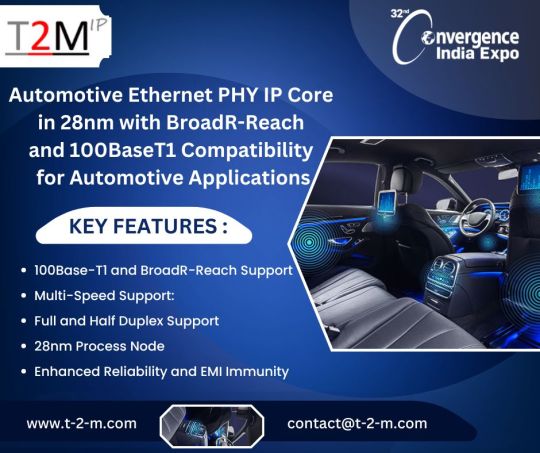
As the automotive industry transitions towards high-speed Ethernet networks, the need for a robust, power-efficient, and scalable Automotive Ethernet PHY solution is critical. The GNET (Giganet Ethernet) IP cores from T2M is designed to support 10M, 100M, and 1000M modes, with both half-duplex and full-duplex functionalities, making it ideal for ADAS, infotainment, and autonomous vehicle applications.
Key Features
100Base-T1 and BroadR-Reach Support: Ensures optimized, cost-effective data communication over a single unshielded twisted pair (UTP) cable, reducing weight and complexity in automotive networks.
Multi-Speed Support: Operates at 10Mbps, 100Mbps, and 1Gbps for flexible and scalable deployment.
Full and Half Duplex Support: Enables diverse automotive communication scenarios for reliable data exchange.
28nm Process Node: Optimized for power efficiency, high performance, and seamless integration into advanced automotive SoCs.
Enhanced Reliability and EMI Immunity: Meets stringent automotive-grade requirements, ensuring optimal signal integrity and robustness in demanding environments.
With 100Base-T1 and BroadR-Reach compatibility, this 1G Ethernet PHY IP is tailored to in-vehicle networking, allowing high-speed, low-latency data transmission. Leveraging 28nm technology, it delivers superior power efficiency, footprint optimization, and high reliability, making it an essential component for connected and autonomous vehicles.
Our GNET IP core, a high-performance Automotive Ethernet PHY, ensures seamless and efficient communication across multiple electronic control units (ECUs), meeting the growing data demands of modern vehicles.
Immediate licensing Availability: These Semiconductor Interface IP Cores are immediately available for licensing as stand-alone IP Cores or with pre-integrated Controllers and PHYs. Please submit a request / MailTo for more information on licensing options and pricing.
About T2M: T2M-IP is a global independent semiconductor technology expert, supplying complex semiconductor IP Cores, Software, KGD, and disruptive technologies to allow faster development of your Wearables, IOT, Automotives, Communications, Storage, Servers, Networking, TV, STB, and Satellite SoCs. For more information, please visit www.t-2-m.com.
1 note
·
View note
Text
16-bit 5MSps SAR ADC in 40nm Node Sets

T2M-IP, the global independent semiconductor IP Cores provider & Technology experts, is proud to announce the availability of latest 16-bit 5MSps Successive Approximation Register (SAR) Analog-to-Digital Converter (ADC) on the 40nm process node. This ADC delivers exceptional performance, flexibility, and efficiency, making it ideal for a wide range of applications, including industrial automation, instrumentation, automotive systems, and IoT devices.
Key Features and Benefits
High Resolution and Flexibility: The ADC offers a full 16-bit resolution with industry-leading linearity, supporting multiple resolution modes (16-bit, 14-bit, 12-bit, and 10-bit) to cater to diverse application requirements.
Superior Dynamic Performance: With an outstanding Signal-to-Noise-and-Distortion Ratio (SNDR) of 82 dB, Total Harmonic Distortion (THD) of -92 dB, and an Effective Number of Bits (ENOB) of 13.5, this ADC ensures unparalleled accuracy and clarity in data conversion.
High-Speed Operation: The ADC supports up to 5MS/s conversion rates, enabling fast and efficient signal processing for time-critical applications.
Enhanced Input Versatility: Rail-to-rail inputs, along with support for single-ended and differential configurations, ensure seamless integration with a wide range of input signals. A 4:1 analog input multiplexer provides additional flexibility.
Advanced Calibration and Correction: An efficient self-calibration engine ensures optimal performance over varying conditions, with built-in offset and gain-error correction enhancing accuracy.
Power Efficiency: With ultra-wide power supply options (1.8V to 3.3V analog and 1.1V ±10% digital), the ADC supports both low-power and high-performance modes, catering to applications requiring extended battery life or peak performance.
Robust Temperature Performance: Designed to operate across a wide temperature range of -40°C to +125°C, this ADC is well-suited for demanding environments.
Versatile Modes for Diverse Applications
The ADC supports single and continuous conversion modes and includes an extended sampling-time option, providing developers with the flexibility to optimize performance and power consumption based on application-specific
requirements.
Applications and Market Impact
This silicon-proven and mass-produced ADC is poised to redefine standards in precision and efficiency, addressing key challenges in next-generation systems. With its scalable performance and flexible architecture, it is an excellent choice for:
Automotive sensors and control systems
Industrial measurement and automation
High-resolution imaging
Wireless IoT devices requiring low power consumption
For more information about the 16-bit 5Msps SAR ADC IP and how it can benefit your projects, or to inquire about licensing opportunities, please contact [email protected]
About T2M: T2MIP is the global independent semiconductor technology expert, supplying complex semiconductor IP Cores, Software, KGD, and disruptive technologies enabling accelerated development of your Wearables, IOT, Communications, Storage, Servers, Networking, TV, STB and Satellite SoCs. For more information, please visit: www.t-2-m.com
Availability: These Semiconductor Analog IP Cores are available for immediate licensing. For more information on licensing options and pricing please drop a request / MailTo
0 notes
Text
ADC IP 14-Bit, 4.32 GSps Silicon-Proven with No Royalty
T2M-IP, the global independent semiconductor IP Cores provider & Technology experts, is pleased to announce the immediate availability of its partner’s 14-bit 4.32Gsps Time-interleaved Pipeline ADC IP Core, fully silicon-proven and whitebox ready for licensing without royalty fees. This cutting-edge technology promises to enhance the performance and efficiency of a wide range of electronic devices, from advanced consumer electronics to critical medical and industrial applications.
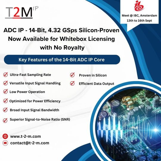
Key Features of the 14-Bit ADC IP Core (Time-Interleaved Pipeline ADC IP):
Ultra-Fast Sampling Rate: Achieves a remarkable 4.32 GSps (Giga-samples per second), ensuring high-resolution data acquisition at unprecedented speeds.
Superior Signal-to-Noise Ratio (SNR): Delivers a 60dBFS SNR (9.7 Effective Number of Bits, ENOB) for input frequencies ranging from 54MHz to 1794MHz, providing excellent signal clarity and accuracy.
Versatile Input Signal Handling: Features external AC coupling for the input signal and supports a 1.0Vpp differential full-scale input, with buffered analog inputs to maintain signal integrity.
Optimized for Power Efficiency: Operates with dual power supplies—1.8V for analog processing and 1.0V for digital compensation—offering a balance between performance and power consumption.
Broad Input Signal Bandwidth: Handles input signals within the 54MHz to 1794MHz range, making it ideal for a wide variety of high-frequency applications.
Low Power Operation: Includes a power-down mode for energy-saving operation, further enhancing its suitability for power-sensitive applications.
Efficient Data Output: Provides 16x14-bit data output at 270 MHz (4.32GHz/16) along with a Data Ready output signal at 270MHz, ensuring seamless integration into high-speed digital systems.
Proven in Silicon: Developed and verified using 28FDSOI technology, this ADC IP has been successfully extracted from a production DOCSIS Tuner STB chip, underscoring its reliability and readiness for deployment in commercial applications.
Availability and Licensing
For more information about the 14-bit 4.32Gsps Time-interleaved Pipeline ADC IP Core and how it can benefit your projects, or to inquire about licensing opportunities, please contact [email protected]
About T2M: T2MIP is the global independent semiconductor technology expert, supplying complex semiconductor IP Cores, Software, KGD, and disruptive technologies enabling accelerated development of your Wearables, IOT, Communications, Storage, Servers, Networking, TV, STB and Satellite SoCs. For more information, please visit: www.t-2-m.com
Availability: These Semiconductor Analog IP Cores are available for immediate licensing. For more information on licensing options and pricing please drop a request / MailTo
0 notes
Text
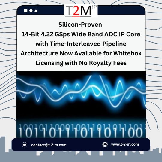
Silicon-Proven 14-Bit 4.32 GSps Wide Band ADC IP Core with No Royalty Fees
T2M-IP, a global leader in semiconductor IP Cores and technology expertise, is pleased to announce the immediate availability of its partner’s new 14-bit 4.32 GSps Wide Band Analog-to-Digital Converter (ADC). This high-speed ADC, which employs a time-interleaved pipeline architecture, is now offered for white box licensing, with no royalty fees, full modification rights, and unlimited usage.
Key Features:
Exceptional Performance: The 14-bit Time-Interleaved Pipeline ADC delivers an impressive 4.32 GSps sampling rate, ensuring optimal performance for demanding applications.
High Signal Fidelity: Achieve a 60 dBFS Signal-to-Noise Ratio (SNR) and 9.7 Effective Number of Bits (ENOB) for input frequencies ranging from 54 MHz to 1794 MHz.
Flexible Input Handling: Supports external AC coupling for the input signal and provides a 1.0Vpp differential full-scale input with buffered analog inputs.
Wide Input Signal Bandwidth: Capable of handling input signals with bandwidths ranging from 54 MHz to 1794 MHz.
Efficient Power Management: Operates on two power supplies – 1.8V for analog circuitry and 1.0V for digital compensation – with an additional power-down mode for energy efficiency.
High Data Throughput: Offers 16x14 bits data output at 270 MHz, along with a Data Ready output at 270 MHz, ensuring seamless data handling and integration.
Silicon Proven Technology: Built on the reliable 28FDSOI process, this ADC has been extracted from a production DOCSIS Tuner Set-Top Box (STB) chip, demonstrating its robustness and performance.
License Flexibility: Available for white box licensing, this ADC comes with no royalty fees and grants full modification rights and unlimited use, allowing developers to customize solutions to their specific needs.
Applications:
This advanced ADC is ideal for a variety of applications, including high-speed communications, digital signal processing, radar systems, and other high-performance electronic systems that require fast and accurate data conversion.
For more information about the 14-bit 4.32Gsps ADC IP Core and how it can benefit your projects, or to inquire about licensing opportunities, please contact [email protected]
About T2M: T2MIP is the global independent semiconductor technology expert, supplying complex semiconductor IP Cores, Software, KGD, and disruptive technologies enabling accelerated development of your Wearables, IOT, Communications, Storage, Servers, Networking, TV, STB and Satellite SoCs. For more information, please visit: www.t-2-m.com
Availability: These Semiconductor Analog IP Cores are available for immediate licensing. For more information on licensing options and pricing please drop a request / MailTo
1 note
·
View note
Text
USB 3.0, PCIe 2.0, SATA 3.0 Combo PHY IP Cores Next Gen Chipsets
T2MIP, the global independent semiconductor IP Cores provider & Technology experts, is pleased to announce the immediate availability of its partner’s Silicon Proven and mature USB 3.0, PCIe 2.0 and SATA 3.0 PHY IP Cores with a successful mass production track record in 22nm Ultra Low Power and 8nm advanced process technology in a wide range of major Fabs. This advanced PHY IP is poised to revolutionize data transfer solutions with its versatile compatibility and power-efficient design, making it ideal for a wide range of applications, from consumer electronics to high-performance computing systems.
Licensed to a host of Global customers, the Combo PHY IP cores integrates three essential high-speed interface standards: USB 3.0, PCIe 2.0, and SATA 3.0 offering extensive compatibility, meeting the full specifications of each protocol. This integration not only enhances device connectivity but also simplifies system design and reduces overall cost. This wide-ranging compatibility ensures that the PHY IP cores can seamlessly integrate into various systems, providing robust connectivity solutions for a multitude of applications. Furthermore, it is fully compatible with the PIPE3.1 interface specification, facilitating seamless integration into diverse system architectures.

One of the standout features of this Combo PHY IP is its configurable data rates, supporting 1.5G, 2.5G, 3G, 5G, and 6G. This flexibility caters to a range of application needs, from low-power devices to high-performance systems. Additionally, it supports both 16-bit and 32-bit parallel interfaces when encode/decode is enabled and a 20-bit parallel interface when bypassed, providing versatility in data processing and transmission. The PHY IP Cores includes PLL control, reference clock control, and built-in power gating, which collectively contribute to significant power savings without compromising performance. It is compatible with various reference clock frequencies, including a 100MHz differential reference clock input or output in PCIe mode, with optional Spread-Spectrum Clock (SSC) support. This capability enhances signal integrity by generating and receiving SSC from 5000ppm to 0ppm. Programmable transmit amplitude and de-emphasis further optimize signal transmission, ensuring reliable and efficient data transfer.
Enhanced detection functions include TX detect RX in PCIe and USB 3.0 modes, Beacon signal generation and detection in PCIe mode, and Low Frequency Periodic Signaling (LFPS) in USB 3.0 mode. The PHY IP cores also excels in power management, supporting L1 sub-state power management and RX low latency mode in SATA operation mode. Built-in testing capabilities, such as Loopback BERT and Multiple Pattern BIST Mode, ensure comprehensive and efficient testing of the PHY IP's functionality.
USB 3.0, PCIe 2.0 and SATA 3.0 Combo PHY IP Cores offers a powerful, flexible, and efficient solution for advanced connectivity needs in 22nm and 8nm SoCs. T2M ‘s broad silicon Interface IP Core Portfolio also includes HDMI, Display Port, MIPI (CSI, DSI UniPro, UFS, RFFE, I3C), PCIe, DDR, 1G Ethernet, V-by-One, programmable SerDes, OnFi and many more, available in major Fabs in process geometries as small as 7nm.
Availability: These Semiconductor Interface IP Cores are available for immediate licensing either stand alone or with pre-integrated Controllers and PHYs. For more information on licensing options and pricing please drop a request / MailTo
About T2M: T2MIP is the global independent semiconductor technology experts, supplying complex semiconductor IP Cores, Software, KGD and disruptive technologies enabling accelerated development of your Wearables, IOT, Communications, Storage, Servers, Networking, TV, STB and Satellite SoCs. For more information, please visit: www.t-2-m.com
1 note
·
View note
Text
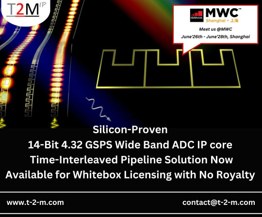
14-Bit 4.32 GSPS ADC IP Available for Whitebox Licensing
T2M-IP, the global independent semiconductor IP Cores provider & Technology experts, is pleased to announce the immediate availability of its partner’s 14-bit 4.32 GSps Wide Band Analog-to-Digital Converter (ADC) utilizing a time-interleaved pipeline architecture. This ADC, designed for high-speed and high-performance applications, is now available for white box licensing with no royalty fees and offers full modification rights and unlimited use.
Key Features:
Exceptional Performance: The 14-bit Time-Interleaved Pipeline ADC delivers a stunning 4.32 GSps sampling rate, ensuring superior performance in demanding applications.
High Signal Fidelity: Achieve a 60dBFS Signal-to-Noise Ratio (SNR) and 9.7 Effective Number of Bits (ENOB) for input frequencies ranging from 54 MHz to 1794 MHz.
Flexible Input Handling: Supports external AC coupling for the input signal and provides a 1.0Vpp differential full-scale input with buffered analog inputs.
Wide Input Signal Bandwidth: Handles input signals with a bandwidth ranging from 54 MHz to 1794 MHz.
Efficient Power Management: Operates on two power supplies – 1.8V for analog circuitry and 1.0V for digital compensation – with an additional power down mode for energy efficiency.
High Data Throughput: Offers 16x14bits data output at 270 MHz, coupled with a Data Ready output at 270 MHz, ensuring seamless data handling and integration.
Silicon Proven Technology: Based on the robust 28FDSOI process, this ADC has been extracted from a production DOCSIS Tuner Set-Top Box (STB) chip, underscoring its reliability and performance.
License Flexibility: Available for white box licensing, this ADC allows for no royalty fees and grants full modification rights and unlimited use, empowering developers to tailor solutions to their specific needs.
Applications:
This advanced ADC is ideal for a range of applications, including high-speed communications, digital signal processing, radar systems, and other high-performance electronic systems requiring rapid and precise data conversion.
For more information about the 14-bit 4.32Gsps ADC IP Core and how it can benefit your projects, or to inquire about licensing options and pricing please drop a request / Mail at [email protected]
About T2M: T2MIP is the global independent semiconductor technology expert, supplying complex semiconductor IP Cores, Software, KGD, and disruptive technologies enabling accelerated development of your Wearables, IOT, Communications, Storage, Servers, Networking, TV, STB and Satellite SoCs. For more information, please visit: www.t-2-m.com
0 notes
Text
eDisplayPort v1.4 Tx PHY and Controller IP Core in 22ULP
T2M-IP, the global independent semiconductor technology expert and leading provider of advanced IP solutions, is excited to announce the release of its silicon-proven DisplayPort v1.4 Transmitter PHY and Controller IP Core, developed in TSMC's 22nm Ultra-Low Power (22ULP) process technology. This innovative IP core delivers exceptional performance and power efficiency, catering to the growing demand for high-quality display solutions in consumer electronics, automotive, and industrial applications.
Our eDisplayPort v1.4 Tx PHY and Controller IP Cores from T2M-IP offer a comprehensive solution, including support for 8K resolution at 60Hz with High Dynamic Range (HDR), Display Stream Compression (DSC) 1.2a, and Forward Error Correction (FEC). The IP core is designed to meet the stringent requirements of modern display applications, ensuring high-speed data transmission with minimal power consumption. TSMC's 22ULP (22nm Ultra Low Power) process technology features ultra-low power consumption, high performance, advanced transistor technology, high density, mixed-signal and RF integration, enhanced design flexibility, and reduced die size, making it ideal for mobile, IoT, and other power-sensitive applications.
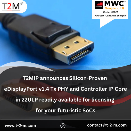
Key features of the DisplayPort v1.4 Tx PHY and Controller IP Core include:
High-Resolution Support: Capable of supporting 8K resolution at 60Hz, providing stunning visual clarity.
Advanced Compression: Integrated Display Stream Compression (DSC) 1.2a for efficient data transmission.
Error Correction: Forward Error Correction (FEC) to ensure reliable data integrity.
Low Power Consumption: Optimized for TSMC's 22ULP process, delivering superior power efficiency.
Broad Compatibility: Fully compliant with the DisplayPort v1.4 specification, ensuring compatibility with a wide range of devices.
Our eDisplayPort v1.4 Tx PHY and Controller IP Cores in TSMC's 22ULP technology. This achievement underscores our commitment to providing cutting-edge IP solutions that meet the evolving needs of our customers. Our DisplayPort v1.4 IP core not only enhances display performance but also significantly reduces power consumption, making it an ideal choice for next-generation display applications. This IP core solution has already undergone rigorous testing and validation to ensure robust performance and reliability. T2M-IP is dedicated to supporting its customers with comprehensive documentation, reference designs, and technical support to facilitate seamless integration and accelerate time-to-market.
Availability: There are so many IP Cores are available for immediate licensing. For more information on licensing options and pricing please drop a request / Mail at [email protected]
About T2M-IP: T2M-IP, is the global independent semiconductor technology expert and leading provider of innovative IP solutions for the semiconductor industry. With a focus on delivering high-performance, power-efficient designs, and empowers customers to develop cutting-edge products for a wide range of applications, including consumer electronics, automotive, and industrial markets. For more information, visit www.t-2-m.com
0 notes