#Angstrom Advanced
Explore tagged Tumblr posts
Visit Tumblr Blog
Explore Tumblr blogs with no restrictions, modern design and the best experience.
Last Seen Tumblr Blogs


Fun Fact
The KCSC sent more than 20K requests to delete posts related to prostitution and porn to Tumblr from January to June 2017.
Note
That Cecil’s kid one was amazing! Could we get a version where Cecil was unfortunately too busy with work to be there for his kid? Maybe they grow up to resent him a little and eventually secretly end up working with the Mauler Twins, Angstrom, etc (maybe even Viltrumites if you’re willing), for their own personal gain, or what ever reasons you see fit? Take your time! Sorry in advance for this request being kinda long :)
Cecil & Villain!Child!Reader
Oh my god i've been wanting to do this request for so long!! Thank you for submitting it!
hcs under the cut
Your mother died young, being a superhero did that.
You never hated her for it, for protecting others and for doing her best
but you couldn't help but resent her a little for who your father was
or rather, who he wasn't
Father was a generous term for what Cecil was. He was a lot of things
Head of the GDA, most powerful non-powered civilian on Earth, a badass ex spy and a great diplomat and genius
but he was NOT a father
you both knew it.
You barely knew the guy, being raised by a nanny specifically for superpowered children like yourself
You saw him occasionally at dinner, but that was maybe once a month.
He, for safety reasons, didn't want the world to know the two of you were related
so naturally, when you had a big baseball game, or your schools talent show cropped up, or even when you landed a main role in your senior play, he "couldn't" attend
Oh sure, it was taped and streamed to him, but you knew he never watched.
So was it really any surprise when you weren't jazzed about becoming a superhero?
When, throughout your final year of high school and the two years after, you befriend the Mauler Twins?
Even supervillains are allowed pen pals in prison, and they made such compelling ones for you to correspond with
It was a fun guessing game as to which twin had written what, and over the course of three years, the three of you had become something akin to friends
They gave you advice on what your major should be, how to handle the stress of college, and shared anecdotes from their own lives
It was hard to imagine them as normal people once, but they made a convincing story
You knew it was likely supervillain manipulation, but they seemed interested in your life, I mean, its not like they had tv
So you would detail your day-to-day life, sharing your frustrations with Cecil and the GDA as a whole
"What an asshole." the three of your would agree
Maybe you three could work together? It was an idea brought up frequently.
So honestly, you weren't really all that surprised when they showed up at your house after getting broke out of prison
Your powers were marginally useful, the ability to phase through walls and be invisible.
It was USEFUL, but not terribly flashy.
Either way, it made stealing things with them incredibly easy.
Cecil didn't notice when you stopped coming home
god knows he was never there
he did notice, however, when the Declaration of Independence went missing
and when GDA specialty supplies went missing
and when the schematics for all sorts of government wherewithal went missing.
"Donald- what the FUCK is going on?!" Cecil demanded, watching the surveillance streams
"Uh- Sir, you need to see this-" The feed was cut and changed to the news
The Mauler twins, business as usual. Whatever.
But-
"OH my god- Y/n?" Cecil put a hand to his head, pacing back and forth
He thought you'd moved out- maybe with roommates or a partner or something- but this?
Oh fuck....
Cecil teleported to the scene, the Mauler Twins and you attempting to break into the White House once more.
"Y/n! Get over here!" Cecil called out, a mix of anger and pain in his voice
you ignored him.
The Guardians of the Globe arrived
and realistically there wasn't a way they could tell them "oh leave that one alone its my offspring."
And so, as all good things go, your villainous spree ended with you in GDA's supervillain prison.
"Why? I want to know why." Cecil sat across from you with his hands folded
"God- what do you care?" you spat back, your hands cuffed and an anti-power collar around your neck
"Because, Y/n, you're my child and I care about you. At the very least I don't want you in prison."
"You didn't even know I had powers."
"Of course I did!"
"You knew I could phase through walls, but being invisible? I've read the files, Mom couldn't do that. And you had no idea I could."
Cecil sat in silence for a minute. Processing.
"Is that what this is, Y/n? Rebellion?"
You shook your head, rolling your eyes "Of course, everything I do is to appease or piss off a guy I don't even know."
"I'm your father, Y/n."
"Fuck off." your glare was cutting, and the tone in your voice oozed venom with every syllable.
"The Mauler Twins helped me enroll in community classes, they gave me advice about being an adult and how the world works. They listened and were happy for me when I graduated. They sent me a shitty graduation card with the supplies you give them in prison. To be clear- these guys were in prison and they showed up more than you did."
Cecil literally couldn't believe what he was hearing.
"Y/n, you're only eighteen, you need to rethink thi-"
"I'm twenty."
Cecil blinked, standing up and going to the door, speaking with Donald through the door before returning
"Twenty.... wow...."
You leveled another glare at him "Yeah. Time flies when you're having fun." your tone was sarcastic, and your disdain apparent.
"Look. I'm sorry for being a bad father, but you're a criminal."
"So? Lock me up, throw away the key. Just fuck out of my life, you were doing so good until now."
Cecil let out a long, drawn out sigh. Feeling twenty years of disappointment in a single moment "Y/n, I know I never took the time to know you, but know this. I don't waste potential."
...
"Go fuck yourself, Cecil."
Bonus!:
The Mauler Twins are being interrogated for their involvement with you
they don't usually take accomplices, so the GDA wanted to know why
instead all they got were violent outburst about your location
"Where is Y/n?! They are INNOCENT damnit! My Clone will agree-!"
"I'm not the clone. But as the ORIGINAL, I demand to know where Y/n is and that they are safe!"
The twins are assured of your safety, but do not calm down until surveillance footage of you and Cecil's interrogation is shown to them
This puts them at ease, as they continue to testify to your innocence.
The GDA has never seen them so concerned about anyone other than themselves
"We will gladly serve our time- god knows we will always find a way out- but Y/n is innocent, release them this instant!"
#invincible#invincible show#invincible season 3#invincible fanfic#invincible spoilers#invincible x reader#cecil stedman#cecil stedman & reader#cecil invincible#invincible cecil#invincible mauler twins#mauler twins
215 notes
·
View notes
Note
I still think about mc and her friends in that really hot, really wild lensless mark story of yours. After clocking Sadie in the face, how did the rest of the friend group react???
And do Lensless Mark, Mohawk Mark and Shiesty Mark really just use super advanced multidimension travel technology just to meet up from time to time to drink beer and play cards?
I think about these things to this day... And lensless' entire brain getting rewired after being praised post-orgasm ofc. Still haunted by how it it was
omggggg yessss i loved that story
i think Lauren wouldn't talk to her at all anymore - probably being a bitch about it too like 'honestly, i always knew there was something off about [y/n]. ASSAULTING Sadie like that? like, wow, grow up.'
Maya, on the other hand, is way more chill about it. even texted you later like 'lauren’s acting like you threw sadie off a balcony. like, girl, it was one punch. calm down lmao'
and yessss i have this little AU headcanon where they didn't all get wrecked in the invincible wars & mohawk has angstrom as his own personal Dr. Strange type lmao. maybe got him to create some type of tech that could open up portals for them & he uses it to meet up with his boys (lensless & shiesty are the only two he fucks with. he used to like emperor but he was kinda too high strung so they all collectively agreed to stop opening portals to his dimension lmfaooo)
#invincible fanfic#invincible x reader#mark grayson x reader#mark grayson fanfic#lensless mark x reader#no goggles mark x reader#whimsical words
84 notes
·
View notes
Note
🥩💖 Hello‼️ I’m a 23yo trans dude looking for 18+ writers for some LONG TERM dead dove/super dark fandom roleplays, specifically Invincible, The Boys, and Cookie Run.
I tend to trans some dude’s genders, which is nonnegotiable!
I really want to have gore, cannibalism, eroguro + snuff, and power imbalances in the roleplay, but obviously, I can adjust accordingly (only regular gore is nonnegotiable for me, sorry). Other things I dig are yandere (although I heavily prefer that the characters are both crazy for each other), dubcon and noncon. All can be discussed later.
I am semi to advanced lit, and I would like my partners to be around the same range. Quality over quantity for me! ALSO, it’s okay if it takes weeks or even months for a partner to reply, as I still will be interested even in their absence. I just need a heads up first.
If you don’t care for the roleplay anymore or lost your muse or something else, I would heavily appreciate it if you’d tell me before leaving. Communication is key.
Smut is a must, but don’t let that think that it will be the only thing happening in the roleplay. I LOVE narratively driven stories, and I write my replies as such (roleplaying multiple characters in a scene is second nature to me and I really don’t mind it, so don’t feel too pressured to mirror me there). For the plots I have in mind, most will have several story arcs, and usually an end goal, but this can all be talked about and discussed!
I prefer wacky AUs to canon divergence, as I love worldbuilding and seeing where everyone would fit inside it. Canon divergence isn’t completely off the table though; I just have a preference. I am in LOVE with the concept of cakeverse and I really want to add those types of elements into the rp, though!
OOC chatter is a MUST, though. I LOVE talking about the rp and how it’s going. I may even draw some stuff too if I’m enjoying it a lot (for some pairings here I will draw ideas/concepts if I think it will help get whatever point across). I want to make friends, not just roleplay like it’s a job.
Now, onto the pairings - highlighted characters are the ones I prefer to muse and italicized characters take higher priority than those that aren’t. If they are both highlighted, then I’m comfortable with either or (some of my top/bot dynamics are not fixed, but my dom/sub dynamics are, just a heads up).
Invincible
Mark Grayson x William Clockwell
•one of my favorite pairings. I’ve been playing around with the idea/AU of an evil/morally dark grey Mark who is a pure-blooded Viltrumite (Debbie is a Viltrumite here) arriving to Earth for the first time with Nolan and Debbie. He meets and saves William his first week on Earth and.. it goes from there.
Mark Grayson x ..Mark Grayson
•Selfcest is so, so good actually - Evil Mark x Good Mark! They get trapped in a dimension together thanks to Angstrom and have to find their way back to their own timelines, but not without fighting first, of course.
Invincible/The Boys
Omni-Man x Homelander
•Another favorite pairing of mine. I have a few plots in mind that are not canon divergent at all (mainly a space pirate au where Homelander is actively getting hunted for various crimes, but I also really like the idea of the two meeting in an MK1 tournament!), but again, everything can be discussed. All I ask for is that Homelander gets manipulated like hell 💖
The Boys
Homelander x Billy Butcher
•I’m still fairly new to this ship (and The Boys parings in general), but I really love their dynamic. There’s no set plot or ideas here, we can brainstorm something together. I would like Billy to be manhandled a little bit ✨
(MALE) Stormfront x Homelander
•Ok I will admit, this is pretty out of left field. I’m a show only, and I recently found out that Stormfront was originally a guy in the comics. I’m aware that the two medias are VERY different in story, but I’d like to combine bits and pieces of both of them into something weird and new, like this version of the ship, for example.
Cookie Run (Kingdom & Tower of Adventures)
Milk Cookie x Dark Choco Cookie
•This is probably one of the few times where I prefer standard yandere dynamics to knife romance or mutual yandere shenanigans. Milk Cookie being absolutely obsessed with and overprotective of his prince.. he’s chasing after him in the pancake tower, trying to reunite with him, maybe. (Also, I’ve been brainstorming a silly superhero au with them and how Dark Choco was once a hero turned evil due to corruption, and Milk is trying to save him/bring him back by any means necessary).
And that’s it! Very long winded of me, sorry about that. Either like this post and I’ll dm you, or just dm me! Ty~
.
#invincible rp#invincible roleplay#the boys rp#the boys roleplay#yandere rp#yandere roleplay#cookie run roleplay#mxm#dark roleplay#dark rp#spicy#dead dove#tw noncon#tw snuff
17 notes
·
View notes
Text
Global Scanning Transmission Electron Microscopy Detector Market: Trends, Growth Outlook 2025–2032
MARKET INSIGHTS
The global Scanning Transmission Electron Microscopy Detector Market size was valued at US$ 156 million in 2024 and is projected to reach US$ 234 million by 2032, at a CAGR of 5.9% during the forecast period 2025-2032. The U.S. market accounted for 32% of global revenue in 2024, while China is expected to witness the fastest growth with a projected CAGR of 7.8% through 2032.
STEM detectors are critical components in electron microscopy systems that enable high-resolution imaging and analytical capabilities at atomic scales. These detectors capture transmitted electrons that have interacted with a thin specimen, providing crucial data for materials characterization. The market comprises two primary detector types: those with field emission guns (FEG) offering superior resolution for advanced research applications, and conventional detectors without FEG used in industrial quality control.
Market growth is driven by increasing R&D investments in nanotechnology and advanced materials development across semiconductor, pharmaceutical, and automotive sectors. Recent technological advancements, such as direct electron detection cameras, have significantly improved detector sensitivity and frame rates. Key industry players including Thermo Fisher Scientific, Gatan, and Hitachi are expanding their product portfolios through strategic acquisitions, with the top five manufacturers collectively holding over 45% market share in 2024.
MARKET DYNAMICS
MARKET DRIVERS
Advancements in Semiconductor Research Fuel Demand for High-Resolution Microscopy
The global semiconductor industry’s relentless pursuit of miniaturization has created unprecedented demand for scanning transmission electron microscopy (STEM) detectors. With semiconductor nodes shrinking below 5nm, traditional microscopy techniques can no longer provide the necessary atomic-level resolution. STEM detectors enable researchers to visualize and analyze materials at sub-angstrom resolutions, making them indispensable for semiconductor defect analysis and materials characterization. The semiconductor industry’s projected growth to over $1 trillion by 2030 directly correlates with increased STEM detector adoption rates in semiconductor fabrication facilities and research institutions globally.
Pharmaceutical Nanotechnology Development Accelerates Market Expansion
Pharmaceutical companies are increasingly leveraging STEM detectors to analyze drug formulations at the nanoscale, particularly for complex biologics and nanoparticle-based drug delivery systems. The ability to characterize particle size distribution, morphology and crystalline structure with atomic precision provides critical quality control parameters for regulatory compliance. With the global nanomedicine market expected to exceed $350 billion by 2030, pharmaceutical manufacturers are investing heavily in advanced microscopy capabilities. Recent FDA guidance on nanotechnology characterization further reinforces this trend, creating sustained demand for cutting-edge STEM detectors in pharmaceutical R&D and quality assurance.
Additionally, academic and government research institutions continue to drive innovation in detector technology. Collaborative projects between national laboratories and private sector manufacturers are pushing the boundaries of detection sensitivity and speed.
➤ For instance, recent breakthroughs in direct electron detection technology have enabled frame rates exceeding 1,600 fps, allowing researchers to capture dynamic nanoscale processes in real-time.
These technological advancements, combined with increasing research funding across multiple industries, are creating a robust growth trajectory for the STEM detector market.
MARKET RESTRAINTS
High Capital Costs and Maintenance Requirements Limit Market Penetration
The sophisticated nature of STEM detectors results in significant financial barriers to adoption. Complete microscopy systems incorporating advanced detectors can exceed $5 million, with annual maintenance costs often reaching hundreds of thousands of dollars. These substantial investments place advanced microscopy capabilities out of reach for many small research institutions and industrial laboratories. Unlike other analytical instruments, STEM detectors require specialized infrastructure including vibration-free environments, stable power supplies, and stringent temperature controls – all of which add to the total cost of ownership.
Other Restraints
Technological Complexity Operation of STEM detectors requires highly trained personnel with specialized expertise in both instrumentation and sample preparation. The steep learning curve associated with these systems leads to extended implementation timelines and increased training costs for adopting organizations.
Sample Preparation Challenges Many potential applications are hindered by the difficulty in preparing samples thin enough for STEM analysis without altering their native properties. These preparation challenges limit the technique’s applicability across certain material classes and biological specimens.
MARKET CHALLENGES
Data Management and Analysis Bottlenecks Constrain Workflows
Modern STEM detectors generate enormous datasets – a single experiment can produce terabytes of raw imaging data. Many research institutions lack the computational infrastructure and analytical tools to effectively process and interpret this volume of information. The high-speed capabilities of next-generation detectors are often underutilized because downstream data pipelines cannot keep pace with acquisition rates. This creates significant workflow inefficiencies and limits the practical application of cutting-edge detector technologies.
Other Challenges
Detector Sensitivity Limitations While significant progress has been made in improving detection quantum efficiency, challenges remain in analyzing beam-sensitive materials. Many organic and biological samples still suffer from radiation damage before sufficient signal can be collected, restricting applications in soft matter research.
Standardization and Interoperability Issues The lack of universal standards for detector interfaces and data formats creates integration challenges when combining components from different manufacturers. This incompatibility increases system complexity and reduces flexibility in microscope configuration options.
MARKET OPPORTUNITIES
Emerging Applications in Battery Technology and Renewable Energy Materials
The global push toward sustainable energy solutions has created significant opportunities for STEM detector applications in battery research and photovoltaic materials development. High-resolution microscopy enables atomic-scale characterization of next-generation battery electrodes, solid-state electrolytes and photovoltaic materials. With governments and private sector investing over $50 billion annually in battery technology R&D, demand for advanced characterization tools continues to accelerate. Detector manufacturers are responding with specialized configurations optimized for energy materials research, including enhanced sensitivity for light elements and improved signal-to-noise ratios for low-dose imaging.
Additionally, corrosion science and materials degradation studies present growing opportunities. Infrastructure modernization initiatives worldwide are driving demand for microscopic analysis of aging mechanisms in structural materials and protective coatings.
The convergence of STEM with complementary techniques such as spectroscopy and tomography is creating new multimodal analysis workflows. These integrated approaches are enabling comprehensive materials characterization that was previously unattainable, opening new application frontiers across multiple industries.
SCANNING TRANSMISSION ELECTRON MICROSCOPY DETECTOR MARKET TRENDS
Technological Advancements in Imaging to Drive Market Growth
The scanning transmission electron microscopy (STEM) detector market is experiencing significant growth due to breakthroughs in high-resolution imaging technologies. Recent innovations in detector efficiency, such as the development of direct electron detection (DED) systems, have improved signal-to-noise ratios by over 30% compared to conventional detectors. Additionally, advancements in pixelated detectors now enable real-time atomic-scale imaging at frame rates exceeding 1,600 fps, revolutionizing materials science research. The integration of artificial intelligence for automated image analysis is further accelerating adoption, particularly in nanotechnology applications where precision is critical. These technological leaps position the market for sustained expansion as research institutions and industrial labs upgrade their microscopy capabilities.
Other Trends
Semiconductor Industry Expansion
With semiconductor nodes shrinking below 5nm, the demand for advanced STEM detectors has surged by approximately 28% annually in chip manufacturing applications. These detectors provide essential characterization capabilities for defect analysis in next-generation semiconductors. Leading foundries are investing heavily in aberration-corrected STEM systems equipped with advanced X-ray detectors to maintain process control. This trend aligns with the global semiconductor market’s projected growth to over $800 billion by 2025, creating sustained demand for precise failure analysis tools throughout the supply chain.
Life Sciences Applications Gaining Traction
The pharmaceutical and biological research sectors are emerging as key growth areas for STEM detectors, driven by increasing investment in structural biology and drug discovery. Recent developments in cryogenic electron microscopy (cryo-EM) techniques have expanded applications in protein structure determination, with global pharmaceutical R&D spending exceeding $200 billion annually. Advanced STEM detectors now enable researchers to visualize molecular complexes at near-atomic resolution, facilitating breakthroughs in targeted drug development. This convergence of microscopy and life sciences is expected to drive nearly 15% annual growth in detector demand from biopharmaceutical applications through 2030.
COMPETITIVE LANDSCAPE
Key Industry Players
Technological Innovation and Strategic Expansion Drive Market Competition
The global Scanning Transmission Electron Microscopy (STEM) Detector market exhibits a moderately consolidated competitive landscape dominated by specialized manufacturers with strong technical expertise. Thermo Fisher Scientific leads the industry, holding approximately 20% market share in 2024, owing to its comprehensive product portfolio and extensive distribution network across 50+ countries.
Gatan (a subsidiary of AMETEK) and Direct Electron have cemented their positions as key innovators, particularly in field emission gun (FEG) equipped detectors. These companies have demonstrated annual R&D investment growth exceeding 12% since 2020, resulting in breakthrough detector resolutions below 0.5 Å.
Meanwhile, emerging players like Quantum Detectors and PNDetector are gaining traction through niche offerings in cryo-STEM applications. Their strategic focus on specimen-sensitive detection systems has secured partnerships with leading research institutions worldwide. Such specialization creates pricing pressures on established players while expanding the total addressable market.
List of Key Scanning Transmission Electron Microscopy Detector Manufacturers
Thermo Fisher Scientific (U.S.)
Gatan (U.S.)
Direct Electron (U.S.)
Delong Instruments (Czech Republic)
El-Mul Technologies (Israel)
Hitachi High-Tech (Japan)
PNDetector (Germany)
Quantum Detectors (U.K.)
Zeppelin Metrology (Germany)
Segment Analysis:
By Type
Field Emission Gun (FEG) Detectors Drive Market Growth with Superior Resolution and Sensitivity
The market is segmented based on type into:
With A Field Emission Gun (FEG)
Subtypes: Cold FEG, Schottky FEG, and others
Without A Field Emission Gun
By Application
Electronics and Semiconductors Lead Due to Critical Need for Nanoscale Imaging
The market is segmented based on application into:
Electronics and Semiconductors
Pharmaceutical Industry
Automotive
Others
By Technology
Energy-Dispersive X-ray Spectroscopy (EDS) Segment Expands with Growing Material Characterization Needs
The market is segmented based on technology into:
Energy-Dispersive X-ray Spectroscopy (EDS)
Electron Energy Loss Spectroscopy (EELS)
Annular Dark Field (ADF) Imaging
Bright Field (BF) Imaging
By End User
Academic Research Institutes Dominate with Extensive Material Science Studies
The market is segmented based on end user into:
Academic Research Institutes
Industrial Laboratories
Government Research Facilities
Private Research Organizations
Regional Analysis: Scanning Transmission Electron Microscopy Detector Market
North America The North American market for scanning transmission electron microscopy (STEM) detectors is driven by robust R&D investments, particularly in the U.S., where academic institutions and semiconductor manufacturers demand high-resolution imaging solutions. The region accounts for approximately 35% of global market revenue in 2024, with field-emission gun detectors dominating due to their superior analytical capabilities. Key players like Thermo Fisher Scientific and Gatan maintain strong footholds here, supported by government funding for nanotechnology research and semiconductor development. However, stringent export controls on advanced detector technologies present regulatory challenges for manufacturers.
Europe Europe maintains a technologically mature STEM detector market, with Germany and the U.K. leading in precision engineering applications for automotive and pharmaceutical research. The region shows growing adoption of direct electron detection systems for cryo-EM applications in life sciences. Collaborative initiatives like Horizon Europe programs are accelerating detector innovation, though market growth faces constraints from reduced public research budgets in Southern Europe. Compliance with EU radiation safety standards adds operational complexity but strengthens product reliability perceptions among end-users.
Asia-Pacific As the fastest-growing regional market, Asia-Pacific is projected to achieve a CAGR exceeding 8% through 2032, propelled by China’s semiconductor fabrication expansion and Japan’s materials science research. Affordable detectors without field emission guns see strong uptake in emerging economies for educational applications, while tier-1 research facilities drive premium segment growth. Local manufacturers like Hitachi are gaining market share through cost-competitive solutions, though intellectual property concerns remain a barrier for Western companies. The region’s electronics boom creates sustained detector demand for failure analysis and nanomaterial characterization.
South America STEM detector adoption in South America remains limited to flagship universities and state-run research centers, with Brazil accounting for over 60% of regional demand. Economic instability restricts capital expenditures on advanced microscopy systems, pushing buyers toward refurbished or entry-level detectors. However, mining and petroleum industries show increasing interest in elemental mapping detectors for materials analysis. Market development faces infrastructure challenges, including unreliable power grids affecting microscope operation in remote research facilities.
Middle East & Africa This emerging market demonstrates potential through strategic investments in Qatar and UAE’s research cities, where STEM detectors support energy and biomedical initiatives. The region shows particular interest in in-situ detectors for catalysis research relevant to oil refining. While South Africa maintains the most established microscopy research community, political uncertainties and currency fluctuations deter large-scale detector deployments. Partnerships with global manufacturers for local service centers are gradually improving market accessibility, though adoption rates remain below global averages.
Report Scope
This market research report provides a comprehensive analysis of the global and regional Scanning Transmission Electron Microscopy (STEM) Detector markets, covering the forecast period 2024–2032. It offers detailed insights into market dynamics, technological advancements, competitive landscape, and key trends shaping the industry.
Key focus areas of the report include:
Market Size & Forecast: Historical data and future projections for revenue, unit shipments, and market value across major regions and segments. The global STEM detector market was valued at USD 126.5 million in 2024 and is projected to reach USD 192.8 million by 2032.
Segmentation Analysis: Detailed breakdown by product type (Field Emission Gun vs Non-Field Emission Gun), application (Electronics, Pharmaceuticals, Automotive), and end-user industries to identify high-growth segments.
Regional Outlook: Insights into market performance across North America (34% market share), Europe (28%), Asia-Pacific (22%), and emerging regions, including country-level analysis of the U.S., China, Japan, and Germany.
Competitive Landscape: Profiles of 9 leading market participants including Thermo Fisher Scientific, Hitachi, and Gatan, covering their product portfolios, R&D investments, and recent M&A activities.
Technology Trends: Assessment of detector sensitivity improvements, AI integration for image analysis, and the shift towards hybrid detector systems.
Market Drivers & Restraints: Evaluation of nanotechnology research funding, semiconductor industry demand versus high equipment costs and technical complexity.
Stakeholder Analysis: Strategic insights for research institutions, OEMs, component suppliers, and investors regarding the USD 45 million annual R&D expenditure in detector technologies.
Related Reports:
https://semiconductorblogs21.blogspot.com/2025/06/global-pecvd-equipment-market-size.htmlhttps://semiconductorblogs21.blogspot.com/2025/06/global-embedded-sbc-market-trends-and.htmlhttps://semiconductorblogs21.blogspot.com/2025/06/global-encoder-chips-market-driving.htmlhttps://semiconductorblogs21.blogspot.com/2025/06/global-bluetooth-audio-chips-and.htmlhttps://semiconductorblogs21.blogspot.com/2025/06/semiconductor-ip-blocks-market-growth.htmlhttps://semiconductorblogs21.blogspot.com/2025/06/global-dc-power-supply-for.htmlhttps://semiconductorblogs21.blogspot.com/2025/06/global-high-voltage-power-supply-for.htmlhttps://semiconductorblogs21.blogspot.com/2025/06/global-industrial-sun-sensors-market.htmlhttps://semiconductorblogs21.blogspot.com/2025/06/global-consumer-grade-contact-image.htmlhttps://semiconductorblogs21.blogspot.com/2025/06/global-non-residential-occupancy.htmlhttps://semiconductorblogs21.blogspot.com/2025/06/global-standalone-digital-signage.htmlhttps://semiconductorblogs21.blogspot.com/2025/06/12-inch-silicon-wafers-market-global-12.htmlhttps://semiconductorblogs21.blogspot.com/2025/06/global-12-inch-semiconductor-silicon.htmlhttps://semiconductorblogs21.blogspot.com/2025/06/global-extreme-ultraviolet-lithography.htmlhttps://semiconductorblogs21.blogspot.com/2025/06/global-industrial-touchscreen-market.htmlhttps://semiconductorblogs21.blogspot.com/2025/06/global-distributed-fiber-optic-sensor.html
0 notes
Text
Global Semiconductor Used High Purity Sputtering Target Material Size, Share & Forecast Report, 2033
Global Semiconductor Used High Purity Sputtering Target Material Market research report provides a complete overview of the market by examining it both qualitatively and statistically, including particular data and in-depth insights from several market segments. While the qualitative analysis of market dynamics, which includes growth drivers, challenges, constraints, and so on, offers in-depth insight into the market's current and potential, the quantitative analysis includes historical and forecast statistics of major market segments. Get Free Request Sample : https://www.globalgrowthinsights.com/enquiry/request-sample-pdf/semiconductor-used-high-purity-sputtering-target-material-market-100124 Who is the Top largest companies (Marketing heads, regional heads) of Global Semiconductor Used High Purity Sputtering Target Material Market?Hitachi Metals, Longhua Technology Group (Luoyang) Co. Ltd., Changzhou Sujing Electronic Material, Materion, Umicore, GRIKIN Advanced Material Co. Ltd., Konfoong Materials International Co. Ltd., JX Nippon Mining & Metals Corporation, Luvata, ULVAC, FURAYA Metals Co. Ltd, Honeywell, Angstrom Sciences, Sumitomo Chemical, Plansee SE, Linde, Advantec, TANAKA, TOSOHMarket Segmentations:On the thought of the product, this report displays the assembly, revenue, price, Classifications market share and rate of growth of each type, primarily split intoMetal Sputtering Target Material, Alloy Sputtering Target Material, Non-metal Sputtering Target MaterialOn the thought of the highest users/applications, this report focuses on the status and outlook for major applications/end users, consumption (sales), market share and rate of growth for each application, includingInjection, Textile, Film, OthersKey Drivers of the Global Semiconductor Used High Purity Sputtering Target Material Market MarketTechnological Innovation: The pulse of the Global Semiconductor Used High Purity Sputtering Target Material Market market is its ongoing technological evolution, enhancing product and service efficiency. Innovations span materials, manufacturing, and digital technologies.Surging Demand: Factors like population growth, urbanization, and shifts in consumer preferences are fueling a rising demand for Global Semiconductor Used High Purity Sputtering Target Material Market products and services, propelling market expansion.Regulatory Encouragement: Supportive government measures, including incentives and regulations favoring Global Semiconductor Used High Purity Sputtering Target Material Market adoptions, such as renewable energy subsidies and carbon pricing, are catalyzing market growth.Environmental Consciousness: The growing awareness of environmental issues and carbon footprint reduction is accelerating the uptake of eco-friendly and renewable. View Full Report @: https://www.globalgrowthinsights.com/market-reports/semiconductor-used-high-purity-sputtering-target-material-market-100124 About Us:Global Growth Insights is the credible source for gaining the market reports that will provide you with the lead your business needs. At GlobalGrowthInsights.com, our objective is providing a platform for many top-notch market research firms worldwide to publish their research reports, as well as helping the decision makers in finding most suitable market research solutions under one roof. Our aim is to provide the best solution that matches the exact customer requirements. This drives us to provide you with custom or syndicated research reports.
#Marketsize#Markettrends#growth#Researchreport#trendingreport#Business#Businessgrowth#businessTrends#GGI#Globalgrowthinsights
0 notes
Text

How Do Viltrumite Powers Work?
How Do the Viltrumite Powers Work? In the comics and the Invincible animated series, we see the incredible powers of this alien race. The "explanation" we're given is that this civilization advanced enormously and developed the biological abilities of its members to the extreme. However, after seeing the incredible abilities of these creatures, it's hard to believe that such powers come from mere biological abilities.
Why don't they use wings to fly? How do they survive in space? And perhaps the most important question: How do they accumulate and unleash such amounts of energy? And perhaps we could generalize the question even further, to the point of asking, where do superheroes in general get such enormous amounts of energy? How can Superman shoot laser beams from his eyes!? How long would he have to absorb the sun's energy to achieve something like that?
This is the english version of a blog post in spanish. If you find any mistake, please leave a comment.
There are cases like Iron Man, where we've already reasoned this out enough. But there are other "superheroes" whose powers are so extreme that they make no sense. In the case of the Viltrumites, however, we could find an explanation, and interestingly, the idea begins with Atom Eve.
Before continuing, let's clarify that we're talking about a completely fictional topic, right? The origin of these powers is entirely in the hands of their creators, in this case, Robert Kirkman. So what follows can only be classified as a "fan hypothesis" and little more.

Cosplay by Kamiko_Zero
Where Do Atom Eve's Powers Come From?
In Atom Eve's origin story, we learn that before she was born, a group of powerful scientists endowed Samantha with the ability to change matter. This ability even allows Eve to fly. However, Eve has blocks that inhibit her from changing living matter, limiting her powers. But under certain extreme circumstances, Samantha is able to overcome these barriers, a detail that will be important for our hypothesis later on…
Despite these explanations, questions remain, for example, where does Eve get the energy to make such changes? Modifying one molecule into another isn't that costly (depending on the molecules). But changing matter at the atomic level is completely different and very costly.
So, let's move on to the next part of the hypothesis.

By gurjeetsingh.art
Parallel Universes in Invincible
As we've seen through the stories of Angstrom Levy and the Flaxans, in Invincible we encounter a variety of parallel universes, and accessing them doesn't seem so difficult.
So the hypothesis would be this: would it be possible that Atom Eve is accessing a parallel universe full of energy? It could be a universe in its infancy, barely emerging from its Big Bang (as in a certain Asimov novel). That could provide her with an enormous amount of energy, and transforming matter would be easy.
How could Eve access parallel universes? In the same way that Angstrom Levy does, using her brain. Perhaps like Freeman Dyson's Quantum Mind Hypothesis. Perhaps quantum phenomena occur in our brains that we don't yet understand, which gives rise to consciousness.
In Atom Eve's case, these quantum phenomena not only give rise to consciousness but also give her access to a parallel universe full of energy, making manipulating matter trivial.
What does this have to do with the powers of the Viltrumites?

Atom Eve's powers and the Viltrumites' powers are different sides of the same coin
Could it be possible that Samantha's powers and those of the Viltrumites are different versions of the same ability? Where Samantha is capable of modifying matter in general, but is limited to inanimate matter, the Viltrumites could have a similar ability, but limited to their own bodies.
This means that they do indeed have access to a parallel universe of immense energy, but are limited to using that energy within the confines of their own bodies. This would allow them to fly and demonstrate enormous strength and endurance, but without being able to modify matter outside of themselves.
We see some clues to this in the Viltrumites' incredible regenerative capacity and their ability to travel through space at enormous speeds for long periods of time.
But perhaps the biggest clue is that the Viltrumites, like Atom Eve, are capable of great feats in emergency situations. This means that they are able to overcome their limitations under certain circumstances.
Could they similarly explain the powers of other heroes in the same universe? Could this be an explanation for the powers of other superheroes outside of this universe? If you think about The Flash and his "Speed Force," there's a certain similarity…
What do you think? Do you think this is a plausible hypothesis? Leave your thoughts in the comments.
1 note
·
View note
Text
The Revolutionary Application of Quartz Plate in Semiconductor Packaging
The Revolutionary Application of Quartz Plate in Semiconductor Packaging: Why These Four Designs Are Game-Changers Let’s cut through the noise: semiconductor packaging isn’t just about chips anymore—it’s about the materials that cradle them. Quartz plates, once relegated to lab equipment, are now the unsung heroes of microelectronics. But not all quartz is created equal.
I’ve seen firsthand how four specific designs—round transparent quartz glass plates, tempered quartz sight glass, OEM customized optical square/round quartz glass plates, and square UV transparent quartz plates—are rewriting the rules of reliability and precision. Here’s why they matter.
1. Round Transparent Quartz Glass Plates: The Purity Powerhouse
Imagine a material so pristine it makes surgical steel look rusty. Round transparent quartz plates, with >99.99% SiO₂ purity, are the gold standard for wafer handling in extreme environments. Take TSMC’s 3nm node fab: by replacing ceramic carriers with these plates, they reduced particulate contamination by 78% during high-temperature annealing1. The secret? Zero metallic ions means no unwanted doping—critical when a single stray atom can wreck a billion-transistor chip.
But purity isn’t their only trick. Their thermal stability (up to 1,200°C) allows rapid thermal processing (RTP) cycles without warping—a feat that aluminum nitride plates fail at after 50 cycles.

2. Tempered Quartz Sight Glass: When Failure Isn’t an Option
Vacuum chambers in EUV lithography systems demand visibility and invincibility. Tempered quartz sight glass, chemically strengthened via ion exchange, laughs at 10⁻⁸ Torr pressures while providing distortion-free inspection windows. ASML’s latest EUV machines use these panels to monitor plasma arcs—where standard fused silica would cloud within weeks under 13.5nm radiation.
The kicker? Their surface hardness (9 Mohs) prevents scratches from robotic handlers—eliminating the “fogged window” failures that once caused 12% of lithography tool downtime.
3. OEM Customized Optical Square/Round Quartz Plates: Geometry Meets Photonics
Why settle for off-the-shelf when light manipulation demands perfection? Customized optical quartz plates, with sub-λ/4 flatness, are enabling breakthroughs in chip-scale photonics. Intel’s optical interconnects team credits square quartz plates—etched with nanoscale grating patterns—for achieving 92% light coupling efficiency in their silicon photonics modules12. The rectangular edges align perfectly with waveguide arrays, something round plates can’t match.
But round variants shine too: their radial symmetry minimizes stress birefringence in laser diode packaging—a must for 800G DR4 transceivers.
4. Square UV Transparent Quartz Plates: The Dark Horse of Advanced Packaging
UV-curing adhesives are the glue holding 2.5D/3D packages together—literally. Square UV quartz plates, transmitting >90% at 254nm, ensure uniform curing while blocking IR heat that warps interposers. Samsung’s HBM4 stack line reported a 30% yield boost after switching to these plates, as their sharp corners align with die edges to prevent adhesive bleed-out.
Bonus: Their UV transparency doubles as a built-in quality check—uncured resin fluoresces under 365nm light, visible through the plate.

Why This Isn’t Just Progress—It’s a Paradigm Shift
Critics argue quartz is “too brittle” or “too niche.” Tell that to the engineers who’ve seen:
Round plates slash cleanroom particle counts by filtering airborne contaminants during robotic transfers.
Square UV plates enable fan-out wafer-level packaging (FOWLP) for wearables, where 0.1mm thickness tolerances are non-negotiable.
While graphene and GaN hog headlines, quartz plates work silently in the trenches—enabling the angstrom-scale precision our connected world demands.
The Bottom Line In semiconductor packaging, the difference between “functional” and “flawless” lies in the materials you trust. These four quartz plate designs aren’t just components—they’re enablers of a future where chips aren’t just smaller, but smarter. If your supply chain hasn’t embraced them yet, you’re not just behind the curve—you’re ignoring the bedrock of modern electronics.
0 notes
Text
Global Top 13 Companies Accounted for 54% of total Liquid Surface Tension Meter market (QYResearch, 2021)
This report studies the Liquid Surface Tension Meter market
Liquid Surface Tension Meter as it applies to physics is a measuring instrument used to measure the surface tension of liquids or surfaces.
The Liquid Surface Tension Meter industry can be broken down into several segments, Static Surface Tension Meter and Dynamic Surface Tension Meter.

According to the new market research report “Global Liquid Surface Tension Meter Market Report 2023-2029”, published by QYResearch, the global Liquid Surface Tension Meter market size is projected to reach USD 0.08 billion by 2029, at a CAGR of 3.3% during the forecast period.
Figure. Global Liquid Surface Tension Meter Market Size (US$ Million), 2018-2029
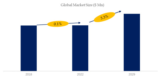
Figure. Global Liquid Surface Tension Meter Top 13 Players Ranking and Market Share(Based on data of 2021, Continually updated)
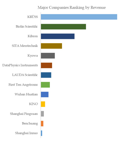
The global key manufacturers of Liquid Surface Tension Meter include KRÜSS, Biolin Scientific, Kibron, SITA Messtechnik, Kyowa, DataPhysics Instruments, LAUDA Scientific, First Ten Angstroms, Wuhan Huatian, KINO, etc. In 2021, the global top five players had a share approximately 54.0% in terms of revenue.
About QYResearch
QYResearch founded in California, USA in 2007.It is a leading global market research and consulting company. With over 16 years’ experience and professional research team in various cities over the world QY Research focuses on management consulting, database and seminar services, IPO consulting, industry chain research and customized research to help our clients in providing non-linear revenue model and make them successful. We are globally recognized for our expansive portfolio of services, good corporate citizenship, and our strong commitment to sustainability. Up to now, we have cooperated with more than 60,000 clients across five continents. Let’s work closely with you and build a bold and better future.
QYResearch is a world-renowned large-scale consulting company. The industry covers various high-tech industry chain market segments, spanning the semiconductor industry chain (semiconductor equipment and parts, semiconductor materials, ICs, Foundry, packaging and testing, discrete devices, sensors, optoelectronic devices), photovoltaic industry chain (equipment, cells, modules, auxiliary material brackets, inverters, power station terminals), new energy automobile industry chain (batteries and materials, auto parts, batteries, motors, electronic control, automotive semiconductors, etc.), communication industry chain (communication system equipment, terminal equipment, electronic components, RF front-end, optical modules, 4G/5G/6G, broadband, IoT, digital economy, AI), advanced materials industry Chain (metal materials, polymer materials, ceramic materials, nano materials, etc.), machinery manufacturing industry chain (CNC machine tools, construction machinery, electrical machinery, 3C automation, industrial robots, lasers, industrial control, drones), food, beverages and pharmaceuticals, medical equipment, agriculture, etc.
0 notes
Text
Aluminum Sputtering Target Market Trends, Regional Segmented, Outlook & Forecast till 2033
The competitive analysis of the Aluminum Sputtering Target Market offers a comprehensive examination of key market players. It encompasses detailed company profiles, insights into revenue distribution, innovations within their product portfolios, regional market presence, strategic development plans, pricing strategies, identified target markets, and immediate future initiatives of industry leaders. This section serves as a valuable resource for readers to understand the driving forces behind competition and what strategies can set them apart in capturing new target markets.
Market projections and forecasts are underpinned by extensive primary research, further validated through precise secondary research specific to the Aluminum Sputtering Target Market. Our research analysts have dedicated substantial time and effort to curate essential industry insights from key industry participants, including Original Equipment Manufacturers (OEMs), top-tier suppliers, distributors, and relevant government entities.
Receive the FREE Sample Report of Aluminum Sputtering Target Market Research Insights @ https://stringentdatalytics.com/sample-request/aluminum-sputtering-target-market/11766/
Market Segmentations:
Global Aluminum Sputtering Target Market: By Company • JX Nippon Mining & Metals Corporation • Praxair • Plansee SE • Mitsui Mining & Smelting • Hitachi Metals • Honeywell • Sumitomo Chemical • ULVAC • Materion (Heraeus) • GRIKIN Advanced Material Co., Ltd. • TOSOH • Ningbo Jiangfeng • Heesung • Luvata • Fujian Acetron New Materials Co., Ltd • Changzhou Sujing Electronic Material • Luoyang Sifon Electronic Materials • FURAYA Metals Co., Ltd • Advantec • Angstrom Sciences • Umicore Thin Film Products Global Aluminum Sputtering Target Market: By Type • Low Purity Aluminum Sputtering Target • High Purity Aluminum Sputtering Target • Ultra High Purity Aluminum Sputtering Target Global Aluminum Sputtering Target Market: By Application • Semiconductors • Solar Cell • Flat Panel Display • Others
Regional Analysis of Global Aluminum Sputtering Target Market
All the regional segmentation has been studied based on recent and future trends, and the market is forecasted throughout the prediction period. The countries covered in the regional analysis of the Global Aluminum Sputtering Target market report are U.S., Canada, and Mexico in North America, Germany, France, U.K., Russia, Italy, Spain, Turkey, Netherlands, Switzerland, Belgium, and Rest of Europe in Europe, Singapore, Malaysia, Australia, Thailand, Indonesia, Philippines, China, Japan, India, South Korea, Rest of Asia-Pacific (APAC) in the Asia-Pacific (APAC), Saudi Arabia, U.A.E, South Africa, Egypt, Israel, Rest of Middle East and Africa (MEA) as a part of Middle East and Africa (MEA), and Argentina, Brazil, and Rest of South America as part of South America.
Click to Purchase Aluminum Sputtering Target Market Research Report @ https://stringentdatalytics.com/purchase/aluminum-sputtering-target-market/11766/
Key Report Highlights:
Key Market Participants: The report delves into the major stakeholders in the market, encompassing market players, suppliers of raw materials and equipment, end-users, traders, distributors, and more.
Comprehensive Company Profiles: Detailed company profiles are provided, offering insights into various aspects including production capacity, pricing, revenue, costs, gross margin, sales volume, sales revenue, consumption patterns, growth rates, import-export dynamics, supply chains, future strategic plans, and technological advancements. This comprehensive analysis draws from a dataset spanning 12 years and includes forecasts.
Market Growth Drivers: The report extensively examines the factors contributing to market growth, with a specific focus on elucidating the diverse categories of end-users within the market.
Data Segmentation: The data and information are presented in a structured manner, allowing for easy access by market player, geographical region, product type, application, and more. Furthermore, the report can be tailored to accommodate specific research requirements.
SWOT Analysis: A SWOT analysis of the market is included, offering an insightful evaluation of its Strengths, Weaknesses, Opportunities, and Threats.
Expert Insights: Concluding the report, it features insights and opinions from industry experts, providing valuable perspectives on the market landscape.
Report includes Competitor's Landscape:
➊ Major trends and growth projections by region and country ➋ Key winning strategies followed by the competitors ➌ Who are the key competitors in this industry? ➍ What shall be the potential of this industry over the forecast tenure? ➎ What are the factors propelling the demand for the Aluminum Sputtering Target? ➏ What are the opportunities that shall aid in significant proliferation of the market growth? ➐ What are the regional and country wise regulations that shall either hamper or boost the demand for Aluminum Sputtering Target? ➑ How has the covid-19 impacted the growth of the market? ➒ Has the supply chain disruption caused changes in the entire value chain? Customization of the Report:
This report can be customized to meet the client’s requirements. Please connect with our sales team ([email protected]), who will ensure that you get a report that suits your needs. You can also get in touch with our executives on +1 346 666 6655 to share your research requirements.
About Stringent Datalytics
Stringent Datalytics offers both custom and syndicated market research reports. Custom market research reports are tailored to a specific client's needs and requirements. These reports provide unique insights into a particular industry or market segment and can help businesses make informed decisions about their strategies and operations.
Syndicated market research reports, on the other hand, are pre-existing reports that are available for purchase by multiple clients. These reports are often produced on a regular basis, such as annually or quarterly, and cover a broad range of industries and market segments. Syndicated reports provide clients with insights into industry trends, market sizes, and competitive landscapes. By offering both custom and syndicated reports, Stringent Datalytics can provide clients with a range of market research solutions that can be customized to their specific needs.
Reach US
Stringent Datalytics
+1 346 666 6655
Social Channels:
Linkedin | Facebook | Twitter | YouTube
0 notes
Text
Nanorobotics Market Industry Remarkable Strong Growth by (2024-2030)
The Nanorobotics Market is estimated to grow from USD 4.9 billion in 2018 to USD 8.3 billion by 2023, at a CAGR of 11.1%. The market is mainly driven by factors such as increasing government support and level of investment in nanorobotics, growing advancements in molecular robots, and rising focus on nanotechnology and regenerative medicine.
Key players in the market are Ginkgo Bioworks (US), Imina Technologies (Switzerland), Thermo Fisher Scientific (US), Klocke Nanotechnik (Germany), Oxford Instruments (UK), Kliendiek Nanotechnik (Germany), Bruker (US), JEOL (Japan), Toronto Nano Instrumentation (Canada), EV Group (Austria), Xidex (US), Synthace (Germany), Park Systems (South Korea), Smaract (Germany), Nanonics Imaging (Israel), Novascan Technologies (US), Angstrom Advanced (US), Hummingbird Scientific (US), NT-MDT Spectrum Instruments (SI) (Russia), and WITec (Germany).
Download PDF Brochure:https://www.marketsandmarkets.com/pdfdownloadNew.asp?id=23476797
Market for magnetically guided nanorobotics to grow at highest CAGR during forecast period
The nanorobotics market for magnetically guided type is expected to grow at the highest CAGR during the forecast period. This is attributed to the ease of use of magnetically guided nanorobotics systems as compared with other nanorobotics types. Globally, several companies and research institutes have developed magnetic manipulation system that uses electromagnetic coils to wirelessly guide nanorobots in several nanorobotics applications. The market for bio-nanorobotics is expected to grow at the second-highest CAGR during the forecast period.
Nanomedicine application to hold largest share of nanorobotics market during forecast period
Nanorobotics is widely used in nanomedicine owning to its healthcare characteristics. Nanomedicine is expected to hold the largest share throughout the forecast period of the overall nanorobotics market, by application. The large share of this application attributes to the large level of commercialization in the healthcare sector for drug delivery, biomaterial, in vivo imaging, in vitro diagnostic, active implants, and drug therapy. The market for biomedical applications accounted for the second-largest share of the overall nanorobotics market, by application, in 2017.
Americas to remain major consumer of nanorobotics during forecast period
The Americas is expected to be a major consumer for nanorobotics solutions during the forecast period. The growth in this market is mainly driven by the favorable government scenario for nanorobotics research and focus on nanotechnology and regenerative medicine. Also, the large share of this region can also be attributed to the highly developed healthcare system and the presence of a large number of nanorobotics players.
0 notes
Text
Meet Quantillion: A Game-Changer In Data Processing And Analytics

In a world where data is the new gold, having the right tools to mine and refine this precious resource is crucial. Enter Quantillion, a groundbreaking software suite by Quantopticon, that’s set to revolutionize the way we handle data processing and analytics.
This isn’t just another tech fad; it’s a seismic shift in how we approach quantum photonics, a field at the bleeding edge of science and technology. So, buckle up, and let’s dive into the fascinating world of Quantillion and explore how it’s reshaping our digital landscape.
The Dawn of a New Era in Quantum Computing
Quantillion isn’t just software; it’s a beacon of innovation in the rapidly evolving realm of quantum computing. This software suite is designed to simulate quantum-photonic devices, a critical component in quantum computers.
Quantum computing, for the uninitiated, is like traditional computing but on steroids. It’s faster, more powerful, and can solve complex problems that are currently beyond our reach.
What makes Quantillion stand out is its ability to model these complex systems with incredible precision. The software is the fruit of 15 years of meticulous development, rooted in advanced quantum mechanical theory. This level of detail means that developers and researchers can predict the behavior of quantum components with unprecedented accuracy.
Bridging the Gap: Quantum-Optical Design Made Simple
Quantillion shines in its ability to simplify the complex world of quantum-optical design. The software specializes in modeling solid-state quantum systems, which are typically embedded in cavity structures. These structures are crucial for controlling and enhancing optical transitions in quantum devices.
The beauty of Quantillion lies in its original and proprietary general methodology. This unique approach, developed by Quantopticon from first principles, saves quantum-optical designers both time and money. How? By eliminating the repetitive cycle of physical experiments needed to test and optimize prototypes.
Accelerating Innovation: A Boon for Academia and Industry
Quantillion is a game-changer for various sectors, from academic research to quantum start-ups and even software design companies. For academics, Quantillion opens new doors to discovering novel quantum phenomena and advancing our understanding of fundamental physics. It’s a tool that promises to push the boundaries of what we know about the quantum world.
Quantillion is key to building top-quality, reliable devices quickly and inexpensively in the realm of quantum start-ups and enterprises. This efficiency is critical in a field where time-to-market can make or break a venture. Additionally, software design companies can quantum-enable their solutions with the Quantillion plug-in, tapping into the burgeoning quantum technologies market.
Quantum-Photonic Device Modeling: A Leap in Precision and Speed
The heart of Quantillion’s prowess lies in its patented fast and accurate algorithm. This algorithm describes cavity quantum electrodynamics with exceptional spatio-temporal resolution, down to the attosecond and angstrom level. For the uninitiated, that’s akin to observing events on tiny scales of time and space: a feat that was once thought impossible.
This high level of precision is essential for rapidly building high-quality, reliable qubits and quantum state control in quantum photonic computers. It’s also crucial for developing single-photon sources for quantum key distribution (QKD) communication systems.
In essence, Quantillion is not just about processing data; it’s about building the very foundations of future quantum technologies.
Cost and Time Efficiency: A Financial Perspective
One of the most compelling aspects of Quantillion is its potential to drastically reduce both time and financial costs. In a field where designing a single-photon source or qubit can take up to 26 weeks, Quantillion cuts this down to just two weeks. Even more impressive is its ability to reduce associated costs by up to 90%.
This efficiency isn’t just impressive; it’s transformative. By replacing costly physical prototypes with Quantillion’s modeling software, businesses and researchers can allocate their resources more effectively, focusing on innovation rather than getting bogged down in lengthy and expensive development cycles.
Empowering Semiconductor Foundries: Boosting Production Yields
Quantillion isn’t just a boon for designers and researchers; it’s also a powerful tool for semiconductor foundries. The software can boost the production yield of quantum-photonic components by more than 1,000 times. This increase is monumental in an industry where even small improvements in yield can translate into significant financial gains.
In the competitive world of semiconductor manufacturing, having a tool like Quantillion could be the key differentiator. It enables foundries to produce more, with higher quality and less waste: a win-win scenario in any production environment.
Conclusion: The Quantum Leap with Quantillion
Quantillion, by Quantopticon, is more than just software; it’s a catalyst for change in the fields of data processing and analytics. Its unparalleled precision in modeling quantum-photonic devices, coupled with its time and cost efficiency, makes it an indispensable tool for anyone venturing into the quantum computing realm.
Whether you’re an academic, a start-up, a software designer, or a semiconductor foundry, Quantillion offers a unique opportunity to be at the forefront of quantum technology development.
As we stand at the brink of a new era in computing and data analytics, Quantillion emerges as a beacon of hope and innovation. It’s not just about processing data faster; it’s about unlocking the mysteries of the quantum world and harnessing its power for the betterment of humanity. With Quantillion, the future is not just bright; it’s quantum.
Read More:
Quantum-Photonic Memories
0 notes
Text
Intel’s AI-Centric Advances: Impact on CPUs and Cloud Services
AI Integration in High-End Processors: Intel’s Meteor Lake CPUs and Server Offerings
In a landscape increasingly dominated by the artificial intelligence (AI) revolution, semiconductor giant Intel has strategically positioned itself at the forefront. This strategic move is evident in their latest offerings, such as the Meteor Lake CPUs, which go beyond traditional processing capabilities. These CPUs feature built-in hardware specifically designed for local AI inference workloads in the PC market. Notably, functions like background blurring in video conferencing can be offloaded to dedicated AI hardware. This not only enhances user experiences but also optimizes the CPU and GPU for other processing tasks, resulting in a faster overall performance and improved battery life for devices.
A parallel initiative is observed in the server market, where Intel’s Sapphire Rapids and Emerald Rapids server CPUs come equipped with AI accelerators. While these CPUs may not match the efficiency of high-powered GPUs, they present a cost-effective solution, especially in light of the increasing rarity and cost of data center GPUs. Intel’s focus on reducing the total cost of ownership is a strategic move aimed at appealing to a broad range of customers.
Competition in the AI Accelerator Space: Intel’s Gaudi Line vs. NVIDIA
The competitive landscape in the high-end processor market intensifies as Intel directly challenges NVIDIA with its Gaudi line of AI accelerators. The latest iteration, Gaudi2, though not as powerful as NVIDIA’s top-tier products, delivers commendable performance. The imminent launch of Gaudi3 later this year further positions Intel as a formidable alternative in the AI accelerator space. This competition is vital for driving innovation and providing consumers with diverse, high-performance options for AI-related workloads.
Semiconductor Manufacturing Advancements: Intel’s Foundry Business and High-NA EUV Machines
Intel’s commitment to staying at the forefront of semiconductor manufacturing is showcased through its foundry business. The rapid rollout of new process nodes, with Intel 4 in mass production and Intel 3 arriving early this year, positions Intel as a key player for AI chip designers seeking advanced manufacturing capabilities. Notably, Intel’s plans for High Numerical Aperture (High-NA) EUV machines signify a pivotal advancement. These machines, with 0.55 numerical aperture optics, are critical for enabling nodes below 2nm/20 angstroms. While High-NA machines won’t be part of the production plans for the upcoming 18A node, they will play a crucial role in Intel’s post-18A node production, referred to as “Intel Next.”
Creation of Articul8: Intel’s Strategic Move into Enterprise AI
Intel’s strategic partnership with digitalbridge has led to the establishment of Articul8, an independent AI company. This move signals Intel’s commitment to expanding its footprint in the AI landscape. Articul8’s platform, optimized for Intel’s server CPUs and Gaudi accelerators, resembles IBM’s WatsonX, indicating a recognition of specific enterprise needs for deploying AI technology. The platform’s focus on security aligns with industry trends, particularly in highly regulated sectors like financial services, where data privacy is paramount.
Intel’s equity stake in Articul8, along with other venture investors, exemplifies a strategic approach to external capital utilization. This strategy allows Intel to refocus its resources on core businesses while maintaining a stake in a promising venture that aligns with its broader objectives. Such moves are not unprecedented for Intel, which previously sought external capital for its automotive chip subsidiary, Mobileye, and spun off its Programmable Solutions group into a standalone business.
Implications for Cloud Service Providers: Enhanced AI Capabilities and Efficiency
As Intel solidifies its position in the AI landscape, cloud service providers are poised to reap the benefits. The integration of AI capabilities into Intel’s processors, coupled with advancements in semiconductor manufacturing, holds significant implications for high-end processor competition. Cloud providers stand to gain from improved AI capabilities, potentially leading to more sophisticated and efficient services. The appeal of Intel’s AI-enabled chips for infrastructure in the cloud service sector is likely to grow, providing a robust foundation for enhanced AI-related workloads and services.
Conclusion
Intel’s strategic focus on AI integration and semiconductor advancements underscores its commitment to staying competitive in the rapidly evolving technology landscape. The implications extend beyond direct competition with industry players, impacting the broader ecosystem, including cloud service providers set to capitalize on enhanced AI capabilities and efficiency.
Source:
https://biz.crast.net/intel-has-found-another-way-to-win-in-the-ai-market-3/
https://www.anandtech.com/show/20066/intel-highna-lithography-update-dev-work-on-intel-18a-production-in-future-node
https://www.anandtech.com/show/21194/asml-ships-first-high-na-euv-scanner-to-intel
This article is re-published from: https://www.scloud.sg/resource/intel-ai-centric-advances-impact-on-cpus-and-cloud-services/
0 notes
Text
Explore Intel Nova Lake CPUs’ 2026 features

2021 was the year that saw the first discovery of information pertaining to the Nova Lake family of processors developed by Intel. Back then, it was projected that the family would debut in 2025 with a significantly revised Core architecture aimed at the desktop enthusiast market. This was the expectation. This would be analogous to the manner in which AMD’s Ryzen processors of the first generation enhanced overall performance.
There have been no new advancements pertaining to this family since the previous update; however, currently, sources close to Moore’s Law Is Dead claim that Nova Lake is still in the works, despite the fact that its launch window has been unexpectedly shifted to H2 2026. MLID also provides a number of preliminary specifications, although it is highly doubtful that these will be finalized at this juncture due to the vast time horizon.
In the second half of the year 2026, Nova Lake, the successor of Arrow Lake Refresh, would be made available for public consumption. It would have up to 180 MB of last level cache, as well as P-cores with a maximum of 16 rentable units, E-cores with a maximum of 32, and LP cores with a maximum of 4. It is possible that it was fabricated utilizing nodes from either Intel’s own 14A manufacturing process or TSMC’s N2P fabrication process.
Even though Intel has claimed that it should no longer be dependent on TSMC’s manufacturing nodes by the year 2025, it looks that Nova Lake may still be built mostly on TSMC’s N2P nodes, if not fully on Intel’s replacement of the 18A node, which MLID refers to as the 14A node. This is despite the fact that Intel has stated that its dependence on TSMC’s manufacturing nodes should halt by the year 2025. Everything rests on whether or not Intel can successfully ramp up manufacturing of angstrom nodes over the next few years.
For the time being, it is projected that Nova Lake will consist of a maximum of sixteen rentable unit performance cores (owing to developments in hyperthreading technology), thirty-two improved efficiency cores known as Arctic Wolf, and four low power efficiency cores. The performance that this core count should deliver should be sufficient to compete with whatever comes after AMD’s Zen6 processors in the year 2026.
This central processing unit (CPU) should be able to compete with whatever comes after AMD’s Zen6 processors because it offers single-thread performance boosts of 20–40% higher than Arrow Lake and a massive boost of 60+% higher than the next Raptor Lake Refresh. It is projected that high-end Core Ultra 9 processors may include as much as 180 MB of cache memory at the very last level, while Core Ultra 7 computers may acquire as much as 144 MB of cache memory.
The information that was received through MLID’s prior leaks indicated that AMD will most likely debut its Zen6 processors by the end of 2025, while the launch of the Zen7 might take place as early as 2027. If Intel were to launch Nova Lake at the end of 2026, the company’s primary objective would be to play catch-up and unseat Zen6 as the market leader, not Zen7.
Because of this, Intel’s release schedule would become wildly out of sync, and the company would continue to lag behind AMD by one step for the foreseeable future. This would put Intel in a worse position than AMD.
0 notes
Text
Ellipsometer Market Size, Type, segmentation, growth and forecast 2023-2030

Ellipsometer Market
The Ellipsometer Market is expected to grow from USD 39.00 Million in 2022 to USD 50.00 Million by 2030, at a CAGR of 3.36% during the forecast period.
Get the Sample Report:https://www.reportprime.com/enquiry/sample-report/11124
Ellipsometer Market Size
An Ellipsometer is an optical instrument that measures the change in polarization of light reflected from a surface to yield information on the physical properties of that surface. The global ellipsometer market research report segments the market based on type, application, region, and market players. The types of ellipsometers covered are Spectroscopic Ellipsometer and Laser Ellipsometer, while the applications investigated include Semiconductors and Electronics, Academia and Labs, Photovoltaics and Solar Cells, and Others. The report also identifies key market players such as J.A. Woollam, Horiba, Gaertner Scientific Corporation, Semilab, Sentech, Holmarc Opto-Mechatronics, Ellitop-Products, Accurion, Angstrom Sun Technologies, and Film Sense operating in the global ellipsometer market. Furthermore, the report provides insights into the regulatory and legal factors dictating market conditions.
Ellipsometer Market Key Player
J.A. Woollam
Horiba
Gaertner Scientific Corporation
Semilab
Sentech
Buy Now & Get Exclusive Discount on this:https://www.reportprime.com/enquiry/request-discount/11124
Ellipsometer Market Segment Analysis
Ellipsometer is an advanced optical measuring instrument that is widely used in the semiconductor industry, pharmaceutical industry, and research laboratories. The global Ellipsometer market is expected to grow steadily due to the increasing demand for efficient and accurate measuring instruments in various industries.
The major factors driving the revenue growth of the Ellipsometer market are the increasing demand for precision optical measurement devices from diverse industries such as electronics, automotive, aerospace, and healthcare, and the rising need for advanced diagnostic equipment for research and development activities.
In addition, the latest trend in the Ellipsometer market is an increasing focus on the development of new optical technologies that provide high precision, improved speed, and accuracy. The incorporation of advanced software and automation in Ellipsometers is also a driving factor for the growth of the market.
However, the major challenges faced by the Ellipsometer market are the high cost of equipment, lack of awareness of the technology, and competition from substitute technologies. The maintenance cost of the equipment and the need for skilled professionals to operate the equipment is also a significant challenge.
The report's main findings reveal that the Ellipsometer market is expected to grow at a CAGR of 8.4% during the forecast period of 2021-2026. The market size is expected to reach USD 762.9 million by 2026 from USD 498.2 million in 2020.
Furthermore, the report recommends that companies operating in the Ellipsometer market should focus on technological advancements, strategic collaborations, and mergers and acquisitions to gain a competitive advantage in the market. Companies should also invest in R&D activities to develop new and innovative technologies that cater to the evolving needs of various industries.
In conclusion, the Ellipsometer market is a promising area with significant potential for growth due to its increasing demand from various industries. However, companies need to overcome the challenges faced by the market to leverage its full potential and gain a competitive advantage.
This report covers impact on COVID-19 and Russia-Ukraine wars in detail.
Purchase This Report:https://www.reportprime.com/checkout?id=11124&price=3590
Market Segmentation (by Application):
Semiconductors and Electronics
Academia and Labs
Photovoltaics and Solar Cells
Others
Information is sourced from www.reportprime.com
0 notes
Text
Atomic Fluorescence Spectrometers In-Depth Profiling With Key Players and Recent Developments, Forecast Period: 2021-2031
Atomic fluorescence spectrometers are devices that determine elements composition by its electromagnetic spectrum. The different atomic weight of elements emits different readings on spectrometer resulting in identification of their composition. The atomic absorption as well as emission find their applications in forensic science analytics, nanoparticle analysis, and molecular tracking.
The advancement of technology and rise in funding of research that offer superior precision and accurate analysis is anticipated to boost the growth of the market. However, complexities associated with accurate measurement and costs involved in atomic fluorescence spectrometers continue to restrain the growth of this market. Opportunities such extensive research in atomic spectroscopy can further improve the scope of atomic fluorescence spectrometers in industrial application.

The global atomic fluorescence spectrometers market is segmented on the basis of technology, application, and geography. By type, the market is divided into atomic absorption spectroscopy, atomic emission spectroscopy, and others. By application, it is classified into pharmaceutical & bio-technology, food & beverage testing, forensic science, petrochemical, and others. By geography, it is analyzed across North America, Europe, Asia-Pacific, and LAMEA.
The key players profiled in the report include Analytik Jena, Angstrom Advanced, Aurora Instruments, Avantes, Lumex Instruments, OVIO Instruments, PerkinElmer, PG Instruments, SAFAS, and Shimadzu.
Full Report With TOC:-https://www.alliedmarketresearch.com/atomic-fluorescence-spectrometers-market
0 notes