#Industrialdesign
Photo
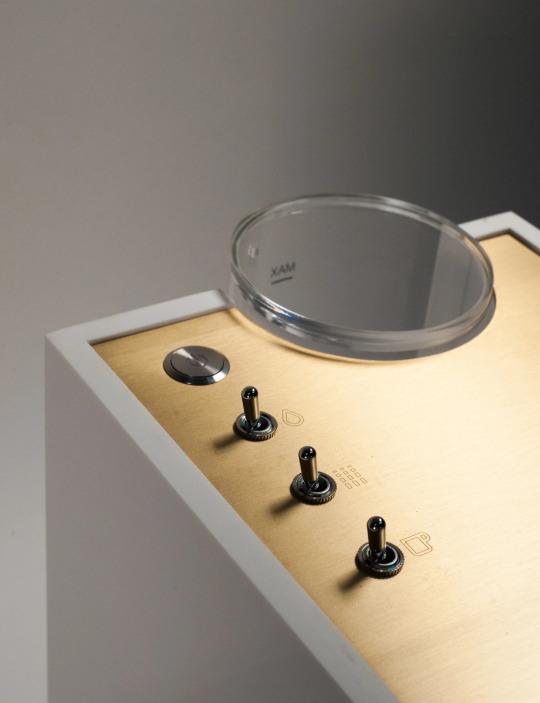
Anza Coffee
https://www.anzacoffee.com/products/anza-white_cf
153 notes
·
View notes
Text

#design#product#concept#furniture#diseño#industrialdesign#productdesign#designer#designideas#designinspiration
30 notes
·
View notes
Text

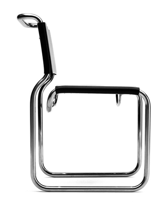
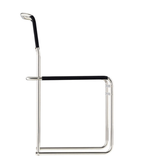
Chairs of Marcel Breuer:
D40, CH66, B40
112 notes
·
View notes
Text

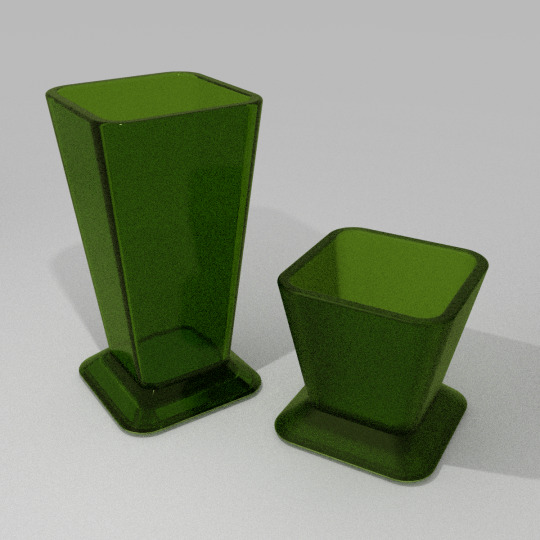

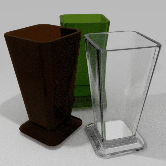

Tablife / differentiate your drinking image
#glasses#design#industrialdesign#angular#square#house#barware#cafeware#houseware#glass#longneck#shortneck#drinking#printable#colorglasses
6 notes
·
View notes
Photo

30 notes
·
View notes
Text

Pencil sword study
Feb 7 2019
#theghostofdash#art#pencil#sketch#sword#weapon#hilt#design#conceptart#conceptdesign#weaponsdesign#drawing#pencildrawing#pencilsketch#industrialdesign#traditionalart#prismacolor#verythin#blade#artistsoninstagram#unicorn#alicorn#prismacolorpencils
2 notes
·
View notes
Photo

Old.s #cardesign #design #automotivedesign #car #carsketch #cardesignworld #sketch #cardesigner #transportationdesign #cars #automotive #cardesigndaily #cardesigncommunity #industrialdesign #cardesignsketch #concept #conceptcar #art #carsofinstagram #supercar #vehicledesign #sketching #drawing #cardrawing #productdesign #autodesign #designer #carart #ferrari #d https://www.instagram.com/p/CpQNLApIPmS/?igshid=NGJjMDIxMWI=
#cardesign#design#automotivedesign#car#carsketch#cardesignworld#sketch#cardesigner#transportationdesign#cars#automotive#cardesigndaily#cardesigncommunity#industrialdesign#cardesignsketch#concept#conceptcar#art#carsofinstagram#supercar#vehicledesign#sketching#drawing#cardrawing#productdesign#autodesign#designer#carart#ferrari#d
44 notes
·
View notes
Text


Seffect / a rounded square cup to enjoy your coffee
#cup#coffee#alatable#coffeetable#cafebar#cafe#coffeeware#barware#servicing#waitering#industrialdesign#design#productdesign#ceramic#printable#espresso#greekcoffee#turkishcoffee#enjoymentfirst#sparetime#leisure#coffeeshop
4 notes
·
View notes
Text
Ultimate Guide to PCB Testing Methods: Ensuring Quality and Reliability in Your Circuits
In the electronics sector, Printed Circuit Boards (PCBs) are the life-lines of virtually all gadgets that are in use in the modern society. From humble home appliances to gigantic industrial equipment, PCBs are the skeletal framework of hardware organization and connection of circuit elements. It is vital to guarantee the quality and dependability of these fundamental parts – thus enters PCB testing methods. It is our hope that this extensive hand will help identify the most suitable test strategies for PCB testing, why these techniques matter, and how to maximize your circuits’ functionality.
Introduction

Firstly, an increase in the capability of different electronic devices leads to higher necessary requirements to the PCBs used in their production. Performing tests on the PCBs is an essential step in the manufacturing process done to confirm that a given board performs as a unit to the expected levels. This guide aims at explaining various techniques of PCB testing with a view of having a better understanding on how to achieve quality and reliability on the circuits.
Why PCB Testing is Crucial

PCB Testing When it comes to the potential defects on PCBs, there are shorts, opens, and some component placements. They can cause device failure, decline in performance level, and sometimes also pose safety issues. Through high-quality testing regimes, it becomes easier to address problems before they reach the customer, and thus manufacturers will have reliable and efficient products. Key reasons for PCB testing include:
Detecting Manufacturing Defects: Solder bridges, missing and placed in wrong position components, all can be detected in the initial stages easily.
Ensuring Functionality: Ensuring that the PCB does what is wanted and needed when it is in use, and under several conditions.
Quality Assurance: Ensuring that the business meets industry standards, and what clients require of them.
Cost Efficiency: Decreasing the likelihood of rework and recall by identifying possible defects before they get to the customer.
Types of PCB Testing Methods
These are the types of PCB Testing Methods:
Visual Inspection

Technique one as also referred to as the VI or visual inspection is the simplest and basic type of testing done on PCBs. The technique entails inspecting the board with naked eyes for some of the common faults including solder bridges, missing parts, and misalignment issues.
Automated Optical Inspection (AOI)

AOI employs cameras and software algorithms to check PCBs for defects and performs the inspections singly. This method of inspection is far more efficient than the manual inspection and simultaneously versatile enough to identify numerous problems.
X-ray Inspection

Some functions which include examination of features of BPCs that could not be easily inspected include solder joints under components through x-ray inspection. It is especially effective in inspecting defects in BGA (Ball Grid Array) and other various packages as well.
In-Circuit Testing (ICT)
ICT entails applying different voltage across the PCB to checks on the electrical characteristics of the needy part and connections. The use of this method is highly recommended for the identification of functional problems and verification of the circuit’s goodness.
Functional Testing (FCT)
Functional testing evaluates the effectiveness of the PCB pointing to the fact that it can be tested when placed in use. This method enables the certification of that the PCB works as expected under actual environment.
Flying Probe Testing
In flying probe testing, the probes are moved around to test the electrical properties of the created PCB. Lower to medium volume production runs can be made easily by using this technique; hence it is advantageous in this regard.
Boundary Scan Testing
Boundary scan testing also called as JTAG testing extends test circuitry into all the components for testing the connections between them. Although, this method is very efficient for identifying connection problems and faults.
Burn-In Testing
Burn-in testing puts the PCB in a state of operational stress for a long time to capture early-life failures. This aspect makes the method reliable for the long term since it is likely to identify problems that may occur when the equipment is in use for a long time.
Detailed Analysis of Each Testing Method works
These are the detailed analysis of each testing method works:
Visual Inspection
Pros:
Simple and low-cost
Determined to be a system for the reporting of noticeable defects as soon as they are observed.
Cons:
Time-consuming for complex boards
Limited to visible defects
Automated Optical Inspection (AOI)
Pros:
Fast and accurate
Is capable of detecting various kinds of defects.
Non-destructive
Cons:
High initial setup cost
May need to have better settings optimized for specific boards.
X-ray Inspection
Pros:
Examines hidden features
Ideal for complex packages
Cons:
Expensive equipment
Requires skilled operators
In-Circuit Testing (ICT)
Pros:
Thorough electrical testing
High fault coverage
Cons:
Requires custom fixtures
Not for all the boards or servers that you wish to build.
Functional Testing (FCT)
Pros:
Ensures real-world performance
Detects system-level issues
Cons:
Time-consuming
The mathematical test object can involve complex arrangements of test configurations.
Flying Probe Testing
Pros:
Flexible and adaptable
Cost-effective for small batches
Cons:
Slower than ICT for big volumes
Applicable only when the board is specially designed
Boundary Scan Testing
Pros:
Interconnections have high fault coverage.
Said; No need to have physical access to the test points
Cons:
Requires boundary scan-enabled components
Complex setup
Burn-In Testing
Pros:
Identifies early-life failures
Ensures long-term reliability
Cons:
Time-consuming and costly
Perhaps stressful to the board
Choosing the Right Testing Method
The choice of the appropriate method of PCB testing can be influenced by several factors such as the level of complexity of the PCB and the numbers of boards to be tested as well as the actual costs of the testing process and other features. Consider the following when choosing a testing method:
Board Complexity: Great board densities or component placement can be a determinant as to whether one needs AOI or X-ray inspection.
Production Volume: Applications that are characterized by high volumes can be easily facilitated by ICT while the low to medium volume applications may require flying probe testing.
Budget: Both manual inspection and AOI are favorable for various production volumes, while X-ray and ICT are more expensive at the beginning.
Specific Requirements: There are two types of the test, namely Functional Test and Burn-In Test that should be made so as to attain the long term reliability in applications that are critical.
Best Practices for PCB Testing
Using the best techniques in testing PCBs increases the quality and reliability of the circuits that you are working on. Here are some key practices to follow:
Early Testing: It is recommended to carry out the tests when the product is still in its design and manufacturing phase so that problems can be noted earlier before they reach a very catastrophic level.
Automate Where Possible: Use method such as automation to reduce the time and improve on the quality of the testing.
Regular Calibration: It is necessary to check if all the testing equipment used for calibration are accurate.
Comprehensive Coverage: This way, you will be able to ensure that there are no defects that are not tested as the best testing approach combines all types of testing methods.
Document Everything: Ensure that you keep records of the tests performed, the results obtained, as well as any measures taken to correct the breaches.
Common Challenges and How to Overcome Them
These are the common challenges and how to overcome them:
False Positives/Negatives
Automated testing methods maybe good some times, they give you the results that are either positive or negative and this will lead to unnecessary rework or more alarming leaving critical defects unfound. In order to avoid this, make sure that testing algorithms and testing equipment are updated and fine-tuned from time to time.
Component Access
Some of the testing techniques involve handling parts of the circuit and with high density board this can be very difficult. Some of the ways in which testbench implementation can be avoided are as follows Boundary scan testing and X-ray inspection.
High Costs
Some form of testing such as X-ray and ICT testing is often very costly. The effectiveness must come with reasonable prices; try to combine some of the mentioned approaches to cover all the aspects without spending too much money.
Future Trends in PCB Testing
About the future, it can be stated that its trends will be in fact linked to the tendencies in technologies and expectations towards ever higher quality and quantity of tested PCBs. Key trends to watch include:
AI and Machine Learning: Using of intelligence algorithms and machine learning in testing algorithms to enhance the efficiency and the minimization of false negative or false positives.
IoT and Smart Manufacturing: Higher testing flexibility and opportunities for the continuous test process supervision.
Advanced Imaging Techniques: The need for better techniques that would enhance the detection of defects within a printed circuit.
Environmental Stress Testing: More focus in the testing of PCBs under different environmental pressures in order to improve on its longevity.
Conclusion
Quality and reliability of packaged circuits have to be maintained to contribute positively in any electronic equipment. This paper seeks to explain the common testing techniques for PCB so that PCB manufacturers are able to test and see if they are free from defects and if they are functional. This ultimate guide will give you a full insight on the available options in PCB testing that will enable you make the best decision that will give you perfect circuits.
The aim is to help you understand how to attain the best quality of PCBs, what methods are worth following, and what trends drive future improvements, thus contributing to the quality of the final electronic products and, consequently, consumer satisfaction.
#PCBTesting#Electronics#CircuitBoard#QualityControl#Engineering#Technology#Manufacturing#IndustrialDesign#Tech#Innovation
2 notes
·
View notes
Text

Keep your tools safe and organized with our stainless steel tool chests. Explore our range of durable and spacious storage options.
#homedecor#pinturaeletrost#industrialdesign#officefurniture#customfurniture#fabrication#industrialfurniture#welding#metal#table#industrial#steelfurnituredesign#stainlesssteel
2 notes
·
View notes
Text
Aluminium flexible duct un-insulated
All sizes
( 4,5,6,8,10,12,14 )
Condition : New: A brand-new, unused, unopened, undamaged item in its original packaging
Type : Ventilation > Ducting, Venting & Accessories > Ducting & Venting
Color : silver
Material : Aluminium
Length : 7.7mtr
Region : UAE
Flexible Duct, For Nominal Duct Diameter 7 in, Wall Thickness 0.125 in, Maximum Temperature Rating 500 Degrees F, Minimum Temperature Rating -100 Degrees F, Insulation Value Not Applicable, Color Silver, Overall Length 15 ft, Duct Material Aluminum, Maximum Pressure Rating 6 in wc, Maximum Air Speed 5, 000 fpm, Vapor Transmission 0.05 Percent, Material Aluminum, Insulation Material Not Applicable, Inside Diameter 7 in, Product Type Non-Insulated Flexible Duct, Compressed Length 30 in
Aluminium flexible ducts, un-insulated, are versatile and essential components in HVAC systems, suitable for various applications across residential, commercial, and industrial settings. These ducts are crafted from lightweight yet durable aluminium, ensuring both flexibility and longevity. Designed to efficiently channel air, they maintain optimal airflow throughout heating, ventilation, and air conditioning systems.

#alramiz#hvac#machines#wholesale#rewinding materials#thermostat#heater & element#tools & safety#are#acsparta#Ducts#ThermalInsulation#CompactSolution#Ventilation#AirHandling#InstallationNeeds#SpaceConstraints#Environment#SizeVariety#Compatibility#HVAC#Efficiency#BuildingDesign#IndustrialDesign#Engineering#Construction#Airflow#EnergyEfficiency#Maintenance#Insulation
2 notes
·
View notes
Photo

Anza Coffee
https://www.anzacoffee.com/products/anza-white_cf
146 notes
·
View notes
Text
Mastering the Art of 3D Scanning: Tips and Tricks for Optimal Results
3D scanning technology has revolutionized various industries, from e-commerce to healthcare. By capturing the physical world in digital form, 3D scanners offer unparalleled precision and detail. Whether you're a beginner or looking to refine your skills, this guide provides essential tips and tricks for mastering 3D scanning.
Understanding 3D Scanners
Before diving into tips, it's crucial to understand the types of 3D scanners available:
Laser Scanners: Use laser beams to measure the distance between the scanner and the object. They are highly accurate and ideal for detailed scans.
Structured Light Scanners: Project a pattern of light onto the object and capture the deformation of the pattern to create a 3D model. They are fast and suitable for a variety of surfaces.
Photogrammetry: Uses photographs from different angles to create a 3D model. This method is cost-effective but requires good lighting and a high-quality camera.
Contact Scanners: Physically touch the object to measure its dimensions. These are less common but very precise.
Tips and Tricks for Effective 3D Scanning
1. Choose the Right Scanner
Selecting the appropriate scanner for your needs is the first step. Consider factors like the object's size, required precision, surface texture, and budget. For instance, laser scanners are excellent for intricate details, while structured light scanners are better for larger objects.
2. Prepare the Object
Proper preparation of the object ensures a smoother scanning process:
Clean the Surface: Dust and dirt can interfere with the scan quality.
Apply Matting Spray: For shiny or reflective surfaces, use a matting spray to reduce glare and improve scan accuracy.
Stabilize the Object: Ensure the object is stable and won't move during scanning.
3. Optimal Lighting
Good lighting is crucial for photogrammetry and structured light scanners. Use diffuse lighting to minimize shadows and reflections. Avoid direct sunlight or harsh lighting, which can create unwanted glare.
4. Correct Positioning
Positioning the scanner and the object correctly is vital:
Maintain a Steady Distance: Keep a consistent distance between the scanner and the object.
Multiple Angles: Capture multiple angles to ensure all parts of the object are scanned. This is particularly important for photogrammetry.
5. Calibration and Testing
Regularly calibrate your scanner to maintain accuracy. Conduct test scans to ensure settings are optimal. Adjust the scanner's resolution and speed based on the object's complexity and desired detail level.
6. Use High-Quality Software
Post-processing software is as important as the scanner itself. Use reputable software to refine the scanned model, remove noise, and fill in any gaps. Some popular software options include:
MeshLab: Free and open-source, great for editing and processing 3D scans.
Blender: Powerful, free software with extensive features for 3D modeling.
Geomagic: Professional-grade software with advanced editing capabilities.
7. Patience and Practice
3D scanning is an art that requires patience and practice. Don’t be discouraged by initial failures. Experiment with different settings, angles, and techniques to improve your skills.
Common Challenges and Solutions
Problem: Incomplete Scans
Solution: Re-scan missing parts from different angles and merge the scans using software.
Problem: Poor Surface Detail
Solution: Increase the scanner's resolution or use a different scanning method.
Problem: Excessive Noise in the Scan
Solution: Use software tools to clean up the noise and smooth the model.
Advanced Tips
Use Turntables
For smaller objects, use a turntable to rotate the object smoothly during scanning. This ensures consistent coverage and saves time.
Leverage Markers
Place markers around the object to help the scanner track its position accurately, especially useful in large or complex scans.
Combine Scanning Methods
For comprehensive results, combine different scanning methods. For example, use a structured light scanner for the object's overall shape and a laser scanner for fine details.
Conclusion
Mastering 3D scanning involves selecting the right equipment, preparing adequately, and refining your technique through practice. By following these tips and tricks, you'll achieve high-quality 3D scans that can enhance your projects and applications. Remember, the key to success in 3D scanning lies in patience, experimentation, and continuous learning. Happy scanning!
#3DScanning#3DScanner#3DScan#3DPrinting#3DModeling#3DTechnology#LaserScanning#StructuredLight#Photogrammetry#3DDesign#DigitalScanning#ScanningTips#TechInnovation#Ecommerce#OnlineStore#EBayStore#ProductPhotography#ProductVisualization#TechTrends#CAD#IndustrialDesign#3DArt#Innovation#TechGadgets#TechNews#DigitalTransformation#TechCommunity#SmartTech#FutureTech#DigitalArt
2 notes
·
View notes
Text
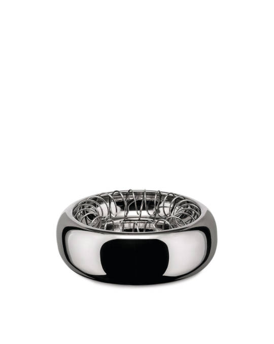


Spirale Ash Tray | Achille Castiglioni for Alessi
67 notes
·
View notes
Text


S-Table XP Lobby
#table#selves#furnituredesign#furniture#design#industrialdesign#interiordesign#productdesign#surface#levels#stationary#PVF_Lobby#type#creativetype#typography#creativetypography#cynfonts
3 notes
·
View notes
Text
Scope Computers
Interior Design Online & Offline Classes
Admission Open
New Batch Start 25/05/2024

#InteriorDesign#HomeDecor#InteriorInspo#Interiors#InteriorStyling#InteriorDesignIdeas#InteriorAndHome#Decor#ModernDesign#BohoDecor#ScandinavianDesign#MidCenturyModern#IndustrialDesign#MinimalistDecor#FarmhouseStyle#EclecticDecor#LivingRoomDecor#BedroomDecor#KitchenDesign#BathroomDesign#HomeOffice#OutdoorLiving#DiningRoomDecor#KidsRoom#SustainableDesign#SmartHome#DIYDecor#VintageDecor#LuxuryInteriors#ColorTrends
2 notes
·
View notes
Last Seen Blogs

sipsofmymiind
you talk pretty

tonym6667
Tonymacias

sewerparty
Welcome to the SewerParty

wildwolfforever
wildwolfforever tumblr post

filataska
Filatáska