#Materials Analysis Using Diffraction
Explore tagged Tumblr posts
Visit Tumblr Blog
Explore Tumblr blogs with no restrictions, modern design and the best experience.
Last Seen Tumblr Blogs


Fun Fact
Hackers stole 65M passwords from Tumblr in 2013.
Text

Cracking the code of performance degradation in solid oxide cells at the atomic level
Researchers have elucidated the mechanism of the initial degradation phenomenon that triggers the performance drop of high-temperature solid oxide electrolysis cell systems, using advanced transmission electron microscopy. Unlike previous studies, which analyzed the final stages of degradation at the micrometer scale, this study successfully verified the initial changes in electrolysis cell materials at the nanometer scale. The research team identified the degradation mechanism occurring between the air electrode and electrolyte of the electrolysis cell through TEM diffraction analysis and theoretical calculations. The observations revealed that oxygen ions accumulated at the interface of the electrolyte, known as Yttria Stabilized Zirconia (YSZ), during the oxygen injection process that that drives the electrolysis reaction. The research is published in the journal Energy & Environmental Science. The research team includes Dr. Hye Jung Chang and Dr. Kyung Joong Yoon of the Hydrogen Energy Materials Research Center at the Korea Institute of Science and Technology.
Read more.
10 notes
·
View notes
Text
Cornell quantum researchers have detected an elusive phase of matter, called the Bragg glass phase, using large volumes of X-ray data and a new machine learning data analysis tool. The discovery settles a long-standing question of whether this almost–but not quite–ordered state of Bragg glass can exist in real materials. The paper, "Bragg glass signatures in PdxErTe3 with X-ray diffraction Temperature Clustering (X-TEC)," is published in Nature Physics. The lead author is Krishnanand Madhukar Mallayya, a postdoctoral researcher in the Department of Physics in the College of Arts and Sciences (A&S). Eun-Ah Kim, professor of physics (A&S), is the corresponding author. The research was conducted in collaboration with scientists at Argonne National Laboratory and at Stanford University.
Continue Reading.
43 notes
·
View notes
Text
Ensuring Weld Quality: Advanced Ultrasonic Testing Methods
In the world of welding, ensuring the quality and integrity of welds is crucial. One of the most effective ways to inspect welds is through ultrasonic testing, which uses high-frequency sound waves to detect imperfections. This blog explores advanced ultrasonic testing methods for welding inspection, highlighting their benefits and applications in the UK.

Introduction to Ultrasonic Testing
Ultrasonic testing for welding involves high-frequency sound waves to detect flaws in welds. This non-destructive testing (NDT) method effectively identifies internal and surface defects without damaging the material.
Why Ultrasonic Testing for Welding?
Accuracy: Provides precise detection of internal flaws.
Non-Destructive: Does not damage the material being inspected.
Versatility: Suitable for a wide range of materials and thicknesses.
Advanced Ultrasonic Testing Techniques
Advanced ultrasonic testing techniques have revolutionised the NDT industry, providing unprecedented levels of accuracy and efficiency. Below are some of the most advanced testing techniques used in the industry:
1. Phased Array Ultrasonic Testing (PAUT)
PAUT is an advanced technique that uses different ultrasonic elements and electronic time delays to create a sweeping beam. This method provides a detailed image of the weld, allowing for precise identification of defects.
Benefits:
High-resolution and detailed images
Faster inspection times
Improved defect characterisation
2. Time-of-Flight Diffraction (TOFD)
TOFD is another complex ultrasonic testing method that uses the time taken by sound waves to travel and diffract around defects to detect and size flaws accurately.
Benefits:
High accuracy in defect sizing
Effective for detecting both surface and subsurface defects
Reduced operator dependency
3. Automated Ultrasonic Testing (AUT)
AUT involves automated systems that perform ultrasonic inspections. This method enhances the consistency and repeatability of inspections, making it ideal for large-scale projects.
Benefits:
Consistent and repeatable results
Increased inspection speed
Reduced human error
Applications of Ultrasonic Testing in the UK
Ultrasonic testing is widely used in the UK across different industries to provide safety and integrity to critical infrastructure. Here are some key applications of ultrasonic testing in the UK.
1. Oil and Gas Industry
In the UK, the oil and gas industry rely heavily on ultrasonic testing for welding to ensure the integrity of pipelines and other critical infrastructure. PAUT and TOFD are commonly used to inspect welds in pipelines, ensuring they are free from defects that could lead to failures.
2. Aerospace Industry
The aerospace industry requires the highest levels of safety and reliability. Ultrasonic testing methods are used extensively to inspect welds in aircraft components, ensuring they meet strict safety standards.
3. Construction and Infrastructure
Ultrasonic testing plays a crucial role in the construction industry, particularly for inspecting welds in bridges, buildings, and other structures.
Advantages of Advanced Ultrasonic Testing Methods
Check out the advantages of advanced ultrasonic testing methods over traditional approaches.
1. Enhanced Accuracy
Advanced ultrasonic testing methods provide higher accuracy in detecting and sizing defects than traditional methods.
2. Increased Efficiency
Automated and advanced techniques like PAUT and AUT significantly reduce inspection times while maintaining high levels of accuracy.
3. Comprehensive Reporting
These methods offer detailed and comprehensive reporting, providing clear images and data that can be used for further analysis and decision-making.
Conclusion
Adopting advanced ultrasonic testing for welding is essential for industries aiming to maintain high quality and safety standards.
Investing in these advanced techniques enhances inspection reliability and ensures compliance with stringent safety regulations. By leveraging the benefits of advanced ultrasonic testing, industries can achieve greater efficiency, accuracy, and overall project success.
9 notes
·
View notes
Text
Helium Spectrum Tube in USA
The observation of atomic emission spectra is one of the few physics demonstrations that captures students' attention. Because of its distinct spectral lines and widespread presence in both terrestrial and cosmic contexts, helium stands out among the other gases that have been examined. With its palpable peek into the quantized nature of atomic energy levels, the Helium Spectrum Tube in USA is a vital tool for both educators and students.

A Helium Spectrum Tube: What Is It?
A glass tube that has been sealed and filled with low-pressure helium gas is called a helium spectrum tube. Electrons in the gas are stimulated to higher energy levels when an electric current flows through it. The atomic emission spectrum of helium is created when these electrons return to their ground state and release light at distinctive wavelengths. The quantized energy levels inside the helium atom are directly depicted visually by this phenomena.
The Emission Spectrum of Helium
The emission spectra of helium is unique and includes multiple prominent lines in the visible spectrum:
Violet at 447 nm
Blue at 469 nm
Blue at 472 nm
Blue-green at 493 nm
Blue-green at 501 nm
Blue-green at 505 nm
Yellow at 587 nm
Red at 669 nm
Understanding atomic structure and quantum mechanics is greatly aided by these lines, which represent transitions between particular energy levels in the helium atom.
Using the Spectrum Tube for Helium
The helium tube is linked to an appropriate power source in order to view the emission spectrum. A spectroscope or diffraction grating can be used to evaluate the light that the tube emits when it is activated. With this configuration, students can measure the emission lines' wavelengths and compare them to the atom's energy transitions.
Applications in Education
In educational settings, the Helium Spectrum Tube in USA is frequently utilized for:
Visualizing how atoms release light at particular wavelengths is known as "atomic emission demonstration."
Understanding electron transitions and energy quantization is essential to teaching quantum mechanics.
Spectroscopic Analysis: Acquiring knowledge about diffraction gratings and spectroscopes.
It offers practical experience with basic ideas in atomic physics and is used in high school and college physics and chemistry curriculum.
Safety Factors
Although it is safe to observe the helium emission spectrum, it is crucial to adhere to the correct safety procedures:
UV Protection: Steer clear of direct exposure to the sun's rays as some spectral lines fall within this region.
Handling: When using the tube, wear the proper eye and skin protection.
Power Supply: To avoid electrical risks, make sure the spectrum tube and the power supply are compatible.
Outside of the Classroom
Beyond classroom environments, the Helium Spectrum Tube in USA exemplifies the following principles:
Astronomy: Knowing the makeup of far-off stars and their stellar spectra.
Astrophysics is the study of the behavior of materials in space and cosmic occurrences.
Environmental science is the study of pollution levels and the makeup of the atmosphere.
Students and scholars can learn more about the basic mechanisms governing the cosmos by examining the emission spectra of different gases, including helium.
Conclusion
A doorway into the quantum universe, the Helium Spectrum Tube in USA is more than just a display in the classroom. It gives the abstract ideas of atomic physics a physical and intelligible appearance with its vivid emission lines. Whether you're a teacher looking to stimulate students' curiosity or a student starting your scientific adventure, the Helium Spectrum
0 notes
Text
How to Check the Purity and Quality of Dolomite Powder

Dolomite powder is a versatile industrial mineral used in construction, agriculture, ceramics, glass, and steel production. Its effectiveness, however, depends heavily on its purity and quality. Impurities or incorrect compositions can compromise product performance and lead to increased costs or defects in the final application.
Whether you're a buyer, manufacturer, or quality control manager, understanding how to check the purity and quality of dolomite powder is essential. Sourcing from a reliable Dolomite Powder Manufacturer in India can ensure you receive consistent, high-quality material—but having your own quality verification methods is always a smart approach.
This article outlines the key indicators and methods used to evaluate the quality and purity of dolomite powder.
What is Dolomite Powder?
Dolomite is a carbonate mineral composed of calcium magnesium carbonate (CaMg(CO₃)₂). When processed into a fine powder, it is widely used as a filler, fluxing agent, or conditioning material. High-quality dolomite powder should contain a balanced proportion of calcium and magnesium carbonates, minimal impurities, and suitable physical properties for the target application.
Why Purity and Quality Matter
Using impure or low-grade dolomite can lead to:
Poor performance in final products
Increased wear and tear in processing equipment
Poor chemical reactivity
Inefficient thermal resistance
Regulatory or quality compliance issues
For industries such as glass, ceramics, or steel, even slight deviations in composition can lead to undesirable results or product failures.
Key Parameters to Check for Quality and Purity
1. Chemical Composition Analysis
A lab analysis using X-ray fluorescence (XRF) or atomic absorption spectroscopy (AAS) can determine the precise chemical makeup of dolomite powder. Key components to look for:
Calcium Carbonate (CaCO₃): Ideally 50–56%
Magnesium Carbonate (MgCO₃): Around 40–45%
Silica (SiO₂): Should be less than 1% for high-purity grades
Iron Oxide (Fe₂O₃): Minimal, usually below 0.3%
Alumina (Al₂O₃): Should be low to prevent contamination in sensitive applications
High-quality dolomite will have a high percentage of CaCO₃ and MgCO₃ with very low levels of other oxides.
2. Physical Properties
a. Whiteness/Brightness
Measured using a whiteness meter or spectrophotometer, high-purity dolomite powder will typically exhibit a brightness of 85–98% (depending on use). This is important in industries like paints, ceramics, and plastics.
b. Particle Size Distribution
Finer powders offer better reactivity and surface area. Check the mesh size or particle size distribution (D50, D97) through laser diffraction methods. A consistent particle size is crucial for uniform mixing and product stability.
c. Moisture Content
Excess moisture can lead to lump formation, microbial growth, or poor dispersion. Dolomite powder should generally have a moisture content below 0.5%.
d. Bulk Density
Bulk density affects packaging, handling, and processing. Standard bulk density for dolomite powder ranges from 0.8 to 1.5 g/cm³ depending on its fineness and grade.
3. Thermal Stability
Dolomite should be tested for decomposition behavior under heat. Thermal gravimetric analysis (TGA) can show how dolomite behaves at high temperatures. For example, decomposition into CaO and MgO occurs at 700–900°C. Stable thermal behavior is crucial in steel, glass, and ceramic industries.
4. Reactivity with Acid
A quick field test involves reacting a sample of dolomite powder with dilute hydrochloric acid (HCl). Pure dolomite will show mild effervescence due to the release of carbon dioxide (CO₂). Vigorous bubbling may indicate excessive calcite or other impurities.
5. X-Ray Diffraction (XRD) Analysis
XRD provides a clear picture of the crystalline phases present in the sample. It helps differentiate between calcite, dolomite, and other minerals. Pure dolomite shows characteristic peaks in its XRD pattern, confirming structural integrity.
6. Visual Inspection
Though basic, visual checks still matter. High-quality dolomite powder should:
Be free from lumps or visible impurities
Have a uniform, light-colored appearance
Feel smooth and powdery (not gritty)
Working with a Trusted Dolomite Powder Manufacturer in India
India is one of the world’s largest producers of dolomite, with widespread availability and advanced mineral processing infrastructure. Partnering with an experienced Dolomite Powder Manufacturer in India offers several advantages:
1. Consistent Quality Control
Top manufacturers adhere to strict quality protocols, conducting chemical and physical analysis at multiple stages—from raw mineral sourcing to final processing.
2. Custom Specifications
Whether you need fine-grade dolomite for glass or coarser material for agriculture, a reliable Indian supplier can tailor properties like particle size, brightness, and chemical composition.
3. Global Standards and Compliance
Reputable Indian manufacturers meet ISO standards and offer documentation like SGS or Bureau Veritas certifications for international buyers.
4. Cost Efficiency
Due to lower extraction and processing costs, Indian dolomite powder is competitively priced, making it ideal for both bulk use and specialized applications.
5. On-Time Delivery and Export Expertise
Many Indian dolomite suppliers have extensive global export networks, ensuring timely delivery, consistent supply, and reliable customer service.
Conclusion
Ensuring the purity and quality of dolomite powder is essential for optimizing performance, reducing costs, and maintaining product integrity across industries. By performing chemical analyses, checking physical properties, and working with trusted suppliers, you can make confident, data-driven decisions about the materials you use.
Choosing a reputable Dolomite Powder Manufacturer in India gives you access to high-purity, application-specific dolomite backed by technical support, customization, and global export capability.
0 notes
Text
Nanoparticle Analysis Market Forecasted to Hit $8.7 Billion by 2034
Nanoparticle Analysis Market is anticipated to expand from $4.1 billion in 2024 to $8.7 billion by 2034, growing at a CAGR of approximately 7.8%. Nanoparticle Analysis Market encompasses the industry dedicated to the characterization and measurement of nanoparticles, crucial for advancing nanotechnology applications. This market includes instruments, software, and services designed to analyze particle size, distribution, and concentration. It serves sectors such as pharmaceuticals, biotechnology, and materials science, facilitating innovation and quality control in product development and manufacturing processes.
To Request Sample Report : https://www.globalinsightservices.com/request-sample/?id=GIS24351 &utm_source=SnehaPatil&utm_medium=Article
The nanoparticle analysis market is witnessing robust growth, propelled by advancements in nanotechnology and increasing applications across various industries. Within the instrumentation segment, electron microscopy leads due to its high-resolution imaging capabilities, while dynamic light scattering is emerging as the second-highest performing sub-segment, driven by its efficiency in particle size analysis. In terms of end-use industries, pharmaceuticals dominate, benefiting from the need for precision in drug development and delivery systems. The biotechnology sector follows closely, with its increasing reliance on nanoparticles for diagnostic and therapeutic purposes.
Regionally, North America commands the market, underpinned by strong research infrastructure and substantial R&D investments. Europe ranks as the second-highest performing region, supported by stringent regulatory frameworks and significant technological advancements. Among countries, the United States stands out due to its leadership in innovation and large-scale adoption of nanoparticle technologies, while Germany follows, driven by its robust industrial base and focus on high-tech manufacturing.
Market Segmentation
Type: Dynamic Light Scattering (DLS), Nanoparticle Tracking Analysis (NTA), Laser Diffraction, Resonant Mass Measurement, Electron Microscopy, Atomic Force Microscopy, X-ray Diffraction
Product: Instruments, Reagents, Kits, Software, Consumables, Accessories
Services: Consulting, Training, Maintenance, Calibration, Customization
Technology: Spectroscopy, Microscopy, Chromatography
Application: Pharmaceutical, Biotechnology, Food and Beverage, Cosmetics, Environmental Testing, Energy, Material Science
Material Type: Metal, Polymer, Ceramic, Composite
End User: Academic Research, Pharmaceutical Companies, Biotechnology Firms, Food Industry, Cosmetic Manufacturers, Environmental Agencies
Functionality: Particle Size Analysis, Zeta Potential Analysis, Molecular Weight Analysis, Concentration Analysis
Installation Type: Portable, Benchtop
Solutions: Complete Systems, Standalone Devices, Integrated Solutions
In 2024, the market demonstrated robust growth, with an estimated market volume of 300 million units. The dynamic segment of particle size analysis currently commands the largest share at 38%, driven by its pivotal role in pharmaceuticals and material sciences. Surface characterization follows closely, holding a 30% share, while zeta potential analysis accounts for 22%. The remaining 10% is distributed among other niche applications. This segmentation underscores the diversified demand across industries, with a notable upsurge in nanotechnology applications.
#nanoparticleanalysis #nanotechnology #particlesizeanalysis #nanoscience #electronmicroscopy #dynamiclightscattering #biotechinnovation #pharmatechnology #materialscience #nanomaterials #researchanddevelopment #drugdelivery #biotechnology #nanomeasurement #labtechnology #scientificresearch #nanoparticles #nanotechsolutions #medicalinnovation #qualitycontrol #pharmaceuticalanalysis #advancedimaging #spectroscopy #microscopy #chromatography #nanotechindustry #scientificinnovation #hightechmanufacturing #chemicalanalysis #particlecharacterization #nanoresearch #industrialanalysis #environmentaltesting
0 notes
Text
Atomic force microscope operates at very close range and without a lens. There are several different types of atomic force microscope, and they all operate by measuring a local property, whether height, optical absorption, or magnetism, using a probe placed very close to the sample. This probe makes it possible to measure qualities over a small area, and an image of that area can be produced that resembles an image on a television screen, consisting of many rows or lines of information placed one above the other. The size of the probe is what generally limits resolution, as opposed to a traditional microscope, where the limitation derives from diffraction effects. When brought close to the sample, the probe measures attractive or repulsive forces between the tip and the sample. The "contact" mode is also called the repulsive mode in which the instrument lightly touches a tip at the end of a leaf spring or "cantilever" to the sample. A raster-scan drags the tip over the sample, and as this occurs, the detection apparatus measures the vertical deflection of the cantilever, indicating the local sample height. This means that in contact mode, the AFM measures hard-sphere repulsion forces between the tip and sample. The probe also works in noncontact mode to derive topographic images from measurements of attractive forces, and in this approach, the tip does not touch the sample. This device is able to produce a resolution of 10 pm. It is superior to electron microscopes in that it can image samples in air and under liquids (Baselt paras. 2-4). The first such device was created "by meticulously gluing a tiny shard of diamond onto one end of a tiny strip of gold foil" (Hong-Qiang Li para. 1). This was in the fall of 1985 as Gerd Binnig and Christoph Gerber used the cantilever to examine insulating surfaces, so that the small hook at the end of the cantilever pressed against the surface while the sample was scanned as the force between tip and sample was measured by tracking the deflection of the cantilever: This was done by monitoring the tunneling current to a second tip positioned above the cantilever. They could delineate lateral features as small as 300 A. The force microscope emerged in this way. In fact, without the breakthrough in tip manufacture, the AFM probably would have remained a curiosity in many research groups. It was Albrecht, a fresh graduate student, who fabricated the first silicon microcantilever and measured the atomic structure of boron nitride. (Hong-Qiang Li para. 1) The tip-cantilever assembly today is usually microfabricated from Si or Si3N4. With further developments, the microcantilevers were perfected. The development of the AFM is part of an ongoing process whereby scientists are trying to analyze smaller and smaller spaces, and the AFM offers many advantages: Scientists are thus gaining new knowledge about how matter operates and interacts at the atomic and molecular level. This means that they can now begin connecting different molecules to one another -- molecules that nature might never have been able to put together. The result will be the creation of entirely new materials, such as a material 100 times stronger than steel but weighing only one-sixth as much. (Uldritch para. 11) Philip Ball emphasizes the importance of the AFM in molecular studies, noting that the AFM "allows researchers to probe the mechanical properties of molecules - how stiff or stretchy they are, for instance. A molecule can literally be grasped at one end by the AFM and pulled like a piece of elastic" (Ball 107). The AFM has its limitations a swell. It is used in the analysis of proteins in medical research, but it cannot provide all the data needed: "The atomic force microscope has resolution sharp enough to see individual atoms but is unable to penetrate below the surface" (Dyson 44). The atomic force microscope has found many uses in different fields. Brian Kooyman notes one use for the AFM in archaeological studies when he writes, The use of the Atomic Force Microscope has allowed Kimball and colleagues to produce textural analysis surface plots that allow them to assess the differences in polish in high and low areas of topography which is critical to success in differentiation of polishes. (Kooyman 159) Ruth Kavenoff points out the use of the AFM in studying the genome, stating that the AFM "can visualize fine details like the two strands of the double helix in small segments of DNA, but they are not suited to DNA molecules as large as the bacterial chromosome" (Kavenoff 37). Another form of this microscope is called the scanning tunneling microscope (STM), which also provides pictures of atoms on or in surfaces. Both types have been used for a variety of purposes, including "to solve processing and materials problems in a wide range of technologies affecting the electronics, telecommunications, biological, chemical, automotive, aerospace, and energy industries. The materials being investigated include thin and thick film coatings, ceramics, composites, glasses, synthetic and biological membranes, metals, polymers, and semiconductors. The AFM is being applied to studies of phenomena such as abrasion, adhesion, cleaning, corrosion, etching, friction, lubrication, plating, and polishing" ("What is an Atomic Force Microscope?" para. 4). The AFM has a laser beam detection system to monitor the bending of the tip, and by this means a topographical image is generated. This imafge is third-dimensional and allows for the measurement of surface features and the generation of surface statistics. One company uses the AFM "to generate pore size distribution data for filtration membranes which is then used in process prediction and optimization. Different AFM imaging modes can be used to optimize the study of different surfaces increasing resolution or accessing further data. Thus the non-contact AFM mode, as its name suggests, allows the imaging of soft easily damaged samples without contact" ("Atomic Force Microscopy" para. 2). Francesc Perez-Murano writes about the use of AFM in the process of nanolithography. This method has been used for two decades in order to define nanometer scale structures and devices: The most common method is based on applying a voltage between the AFM tip and the surface: the presence of humidity in the air induces local oxidation of the surface. The resulting thin oxide layer forms itself into a nanostructure, or can serve as a mask for subsequent selective etching of the surface. (Perez-Murano para. 1). The author notes a new but related use of AFM for a process known as PMMA Polymethyl-methacrylate). The general ability of AFM to oxidize materials has been used to fabricate structures on many materials: Now we have applied the same technique to thin layers of PMMA. PMMA is particularly relevant to nanotechnology as it's used as a resist material for electron beam lithography. The PMMA is locally exposed to a beam of electrons, changing its properties and making it solvent in a convenient developer. With AFM nanolithography, we have obtained at least the same resolution as with electron beam lithography systems, which are not as readily available as AFM in research laboratories. What's more, there is no need for a development process since the PMMA is directly eliminated. (Perez-Murano para. 2) Other methods have been used for scratching the PMMA by exerting a high force with the AFM tip, but this new approach involves a new mechanism responsible for eliminating the PMMA: "As confirmed by electrical measurements, the process involves an electrochemical reaction that causes the PMMA to dissolve" (Perez-Murano para. 3). The work is of interest both from a practical point-of-view - combination with electron beam lithography is already demonstrated - as well as for fundamental reasons - it identifies a new mechanism of surface modification. Because AFM operates without damaging the material being analyzed, this method has been widely used for analyzing biological materials. In order to understand biological systems, their structure must be understood, and structural biology is the study of the structure and function of components of living systems. The AFM is a vital tool for analyzing the surface topography of native biomolecules at subnanometer resolution: Unlike X-ray crystallography and electron microscopy (EM), the AFM allows biomolecules to be imaged not only under physiological conditions, but also while biological processes are at work. Because of the high signal-to-noise (S/N) ratio, the detailed topological information is not restricted to crystalline specimens. Hence single biomolecules without inherent symmetry can be directly monitored in their native environment. (Miller, Aebi, and Engel para. 1) The AFM can also offer data on the binding properties of biological systems, such as the specific interaction between two kinds of molecules. This can be accomplished by binding one kind of molecule to the top of the cantilever and the other on the surface of the sample support: The adhesion force upon separation is then a measure of the binding strength. This method allowed the intermolecular forces between individual ligand-receptor pairs... complementary DNA strands... cell adhesion proteoglycans... And the specific antigen-antibody interaction... To be determined. (Miller, Aebi, and Engel para. 2) An advantage of the AFM is that it can analyze native tissue directly without prior dehydration, useful for such investigations as that of articular cartilage which has to be kept in physiological buffer to preserve its ultrastructure. Surface irregularities are often seen when using the scanning electron microscope, but these are absent using the AFM. One such analysis is described below: Occasionally, the cartilage surface exhibits local discontinuities where an underlying fibrous network is distinguishable. Digestion of the cartilage surface with chondroitinase AC exposes this fibrous network more systematically so that the individual fibers are visualized with great clarity by AFM. When imaged at higher magnification, these distinct fibers exhibit a 60nm repeat, indicating that they are assembled from collagen fibrils. (Miller, Aebi, and Engel para. 4) The AFM has been shown to be valuable in similar analyses of biological materials and processes. While AFM images also offer a view of the atomic detail of solids, the process is not useful for analyzing biomolecules such as proteins because they are designed to undergo conformational changes and form flexible supermolecular assemblies, meaning they are mechanically "soft" so that the surface cannot be probed for atomic detail. However, as Miller, Aebi, and Engel note, "state-of-the-art specimen preparation and instrumentation now allow the surface topography of native proteins to be imaged at subnanometer resolution" (para. 5). A recent example of biological research using the AFM comes from Santa Barbara, California, where researchers used the AFM to discern unique properties of bone: Collagen, the most abundant protein in the human body -- serving as a structural component of a variety of tissues including bone, tendon and skin -- reveals special properties which allow it to "bounce back" when pulled or stressed in laboratory experiments. The AFM operates by tapping and pulling with a tiny needle. ("Bone Strength Probed by Scientists" para. 1) This research shows that the collagen in bone contains sacrificial bonds that rupture as the collagen is stretched, and these ruptures then heal. The purpose of these bonds is to provide a means for dissipating mechanical energy in collagen molecules (("Bone Strength Probed by Scientists" para. 2). AFMs constitute a subset within the larger group known as scanning-probe microscopes, which can utilize many different types of tips to measure electrical, mechanical, or magnetic properties. Tips exist that can perform simultaneous dimensional and electrical measurements. It is when a scanning-probe microscope uses a tip that can discern properties at the atomic level that the instrument becomes an atomic-force microscope. Such devices can measure features within a few Angstroms and do so without harming the sample. As on scientist notes, "Manufacturers need to perform nondestructive measurements in all three dimensions to ensure their device geometries fall within ever-smaller tolerances" (Titus para. 4). Another company uses AFM to detect flaws in surface-acoustic-wave devices, defects that cannot be seen with an optical microscope. The same company uses AFM to check the results of steps in photolithograpy (Titus paras 5-6). Kevin Kjoller considers how to measure the true resolving power of an atomic force microscope, noting first that resolution means the same as it does for an optical microscope, meaning the minimum distance between two adjacent objects that a microscope can identify as separate. Kjoller complains that most manufacturers substitute some meaningless term for resolution and ignore the reality. Several issues need to be considered, such as the size of the probe and three types of limiting noise, electical, mechanical, and acoustic. Kjoller defines electtical noise as "the sum of the thermal and operating noise from all components inside the AFM electronics, including any noise due to cross-talk and less-than-optimal grouping" (Kjoller para. 7). Mechanical noise can be particularly harmful and may derive from the mechanical path length between the probe and the sample. Acoustic noise means that the system generates noise, and this can be eliminated with a well-designed and well-implemented acoustic isolation environment" (Kjoller paras. 8-9). The accuracy of the AFM depends on the state of the tip, and a worn tip can produce blurred images ("V-shaped Tips Blur Microscopy" paras. 1-7). Efforts to control for this include the recent development of an automatic tip evaluation system showing when the tip needs to be replaced ("Automatic Tip Evaluation Broadens AFM Applications" para. 1). More and more applications for the AFM are developed all the time. Scientists have found many ways to make use of the unique capabilities of this system to analyze different substances down to the atomic level. References Automatic Tip Evaluation Broadens AFM Applications." R & D (1 July 1998). September 15, 2005. http://www.highbeam.com/library/doc3.asp?DOCID=1G1:21007984&num=31&ctrlInfo=Round17ProdSRResult&ao=&FreePremium=BOTH. Atomic Force Microscopy." 2005. September 16, 2005. Ball, Philip. Molecules. Oxford: Oxford University Press, 2003. Baselt, David. "How AFM Works." Atomic Force Microscopy. 1993. September 16, 2005. http://stm2.nrl.navy.mil/how-afm/how-afm.html#Generalconcept. Bone Strength Probed by Scientists: Atomic Force Microscope Reveals 'Sacrificial Bonds' in Bone Collagen." Ascribe Higher Education News Service (12 Dec 2001). September 16, 2005. http://www.highbeam.com/library/doc3.asp?DOCID=1G1:80759635&num=27&ctrlInfo=Round17ProdSRResult&ao=&FreePremium=BOTH. Dyson, Freeman J. The Sun, the Genome & the Internet: Tools of Scientific Revolutions. New York: Oxford University Press, 1999. Hong-Quiang Li. "Introduction." Atomic Force Microscopy Student Module. 1997. September 15, 2005. http://www.chembio.uoguelph.ca/educmat/chm729/afm/introdn.htm. Kjoller, Kevin. "Judging AFM Performance." R & D (1 Aug 2000). http://www.highbeam.com/library/doc3.asp?DOCID=1G1:65189799&num=24&ctrlInfo=Round17ProdSRResult&ao=&FreePremium=BOTH. Kooyman, Brian P. Understanding Stone Tools and Archaeological Sites. Calgary, Alberta: University of Calgary Press, 2000. Muller, Daniel J., Ueli Aebi, and Andreas Engel. "Imaging, Measuring and Manipulating Native Biomolecular Systems with the Atomic Force Microscope." 1996. September 16, 2005. http://www.mih.unibas.ch/Booklet/Booklet96/Chapter3/Chapter3.html. Perez-Murano, Francesc. "Nanolithography of PMMA Using Atomic Force Microscopy." (4 July 2005). September 16, 2005. http://nanotechweb.org/articles/journal/4/7/1/1. Ravenoff, Ruth. "Portrait of a Genome." Art Journal, 55(1)(1996), 37. Titus, Jon. "AFMs Pinpoint Surface Defects: When Optical Inspection Fails to Uncover Defects, You Can Turn to an Atomic Force Microscope to Scan a Sample's Surface." Test & Measurement World (2004, March 1). September 17, 2005. http://www.highbeam.com/library/doc3.asp?DOCID=1G1:118793765&num=2&ctrlInfo=Round17ProdSRResult&ao=&FreePremium=BOTH. Uldrich, Jack. "Why Nanotechnology Will Arrive Sooner Than Expected." The Futurist.36(2)(March-April 2002). September 16, 2005. http://www.questia.com/PM.qst?a=o&d=5000698146. V-shaped Tips Blur Microscopy." Chemistry and Industry (17 March 2003). September 15, 2005. http://www.highbeam.com/library/doc3.asp?DOCID=1G1:99773234&num=37&ctrlInfo=Round17ProdSRResult&ao=&FreePremium=BOTH. What is an Atomic Force Microscope?" The University of Toledo College of Engineering (2005). September 16, 2005. http://www.che.utoledo.edu/nadarajah/webpages/whatsafm.html. Read the full article
0 notes
Text
Particle Size Analysis Market worth $596 million by 2028
Particle Size Analysis Market in terms of revenue was estimated to be worth $446 million in 2023 and is poised to reach $596 million by 2028, growing at a CAGR of 6.0% from 2023 to 2028 according to a latest report published by MarketsandMarkets™. Market growth is attributed to the Escalating investments in research and development within the pharmaceutical sector, driving market expansion.
Download an Illustrative overview: https://www.marketsandmarkets.com/pdfdownloadNew.asp?id=74084833
Based on the technology, the particle size analysis market is segmented into laser diffraction, dynamic light scattering, imaging, coulter principle, nanoparticle tracking analysis, sieve analysis, and other technologies. The nanoparticle tracking analysis (NTA) technology segment is expected to witness the highest growth rate during the forecast period 2023 to 2028. The advanced capabilities provided by NTA find primary application in the biopharmaceutical and biotechnology sectors. The growing research and development efforts within the biopharmaceutical industry underscores the expanding utility of this technology.
Based on dispersion type, the particle size analysis market is segmented into wet dispersion, dry dispersion, and spray dispersion. Wet dispersion segment is expected to register the highest growth rate during the forecast period 2023 to 2028. The substantial growth rate in this market segment is primarily driven by the expanding range of applications for nanoparticles, predominantly assessed through liquid dispersion methods.
Based on type, the particle size analysis market is segmented into the particle size analysis market is further segmented further into bench-top analyzers and portable analyzers. Bench- top analyzer is expected to register the highest growth rate during the forecast period 2023 to 2028. High levels of efficacy and adaptability are evident in a variety of applications, including point-of-care diagnostics, pharmaceutical research, environmental analysis, food safety, material science, biotechnology, cannabis testing, and the characterization of nanomaterials are expected to be key drivers of market growth.
Based on end users, the particle size analysis market is segmented into healthcare industry, cosmetic industry, chemical and petroleum industry, mining, minerals, and cement industry, food and beverage industry, other industries (include industries related to inks, toners, paints, coatings, and environmental analysis, among others. The healthcare industry is expected to register the highest growth rate during the forecast period 2023 to 2028. The growing utilization of nanotechnology in the realm of medical science, the surging expansion of pharmaceuticals within the healthcare sector, and the rising prevalence of analytical laboratories all mark notable developments are expected to be key drivers of market growth.
Based on region, the particle size analysis industry is segmented into North America, Europe, Asia Pacific, Latin America, and Middle East & Africa. The North America particle size analysis market is anticipated to register the highest growth during the forecast period 2023 to 2028. The growing government backing for nanotechnology research and the escalating proliferation of stringent regulatory standards regarding product quality within the pharmaceutical and food & beverage sectors are major factors responsible for the growth of the market.
Buy a Particle Size Analysis Industry Report (204 Pages PDF with Insightful Charts, Tables, and Figures): https://www.marketsandmarkets.com/Purchase/purchase_reportNew.asp?id=74084833
Particle Size Analysis market major players covered in the report, such as:
Spectris (UK),
HORIBA (Japan),
Danaher (US),
Anton Paar GmbH (Austria),
Bettersize Instruments Ltd. (China),
Brookhaven Instruments (US),
Fritsch GmbH (Germany),
LS Instruments (Switzerland),
Metller Toledo (US),
Micromeritics Instrument Corporation (US),
Microtrac Retsch GmbH (Germany),
Sympatec GmbH (Germany),
TSI (US),
and Among Others
Request for FREE Sample Pages: https://www.marketsandmarkets.com/requestsampleNew.asp?id=74084833
This report has segmented the particle size analysis market based on technology, dispersion, type, end-user, and region.
Particle Size Analysis Market, by Technology
Laser Diffraction
Dynamic Light scattering
Imaging
Dynamic Imaging
Static Imaging
Nanoparticle Tracking Analysis (NTA)
Coulter Principle
Sieve Analysis
Other Technologies
Particle Size Analysis Market, by Dispersion
Wet Dispersion
Dry Dispersion
Spray Dispersion
Particle Size Analysis Market, by Type
Bench-Top Analyzers
Portable Analyzers
Particle Size Analysis Market, by End User
Healthcare Industry
Pharmaceutical & Biotechnology Companies
Public & Private Institutions
Academic Institutions
Cosmetic Industry
Chemicals & Petroleum Industry
Mining, Minerals and Cement Industry
Food & Beverage Industry
Other Industries
Particle Size Analysis Market, by Region
North America
US
Canada
Europe
Germany
France
UK
Spain
Italy
Rest of Europe
Asia Pacific
Japan
China
India
Australia
South Korea
Rest of Asia Pacific
Latin America
Brazil
Mexico
Rest of Latin America
Middle East and Africa
Get 10% Free Customization on this Report: https://www.marketsandmarkets.com/requestCustomizationNew.asp?id=74084833
Recent Developments
In August 2023, Anton Paar GmbH introduced Litesizer DIA 500, the latest addition to the Particle Analysis & Surface Charge (PC) product line. This innovative instrument brings dynamic image analysis to your fingertips, allowing for precise measurement of particle size and shape within the range of 0.8 µm to 8,000 µm. With 1 µm equaling 0.001 millimeter.
In May 2023, The Verder Group has acquired France’s Formulaction S.A. and will integrate it into Microtrac MRB, a prominent manufacturer of Particle Characterization Systems within the group’s Scientific Division.
In March 2022, Aerolase is expanding its services beyond aesthetic treatments to help dermatologists with different focuses. They will now offer treatments for conditions like vitiligo, leukoderma, and atopic dermatitis. They’re also working on getting FDA clearance for treating alopecia areata in 2023, using technology that has already been proven effective in Europe and other places. These additions will complement their existing treatments for acne, psoriasis, and rosacea.
0 notes
Text
Failure Analysis Experts: Forensic Investigations of Materials & Structures
In today’s world, materials and structures play a crucial role in everything from industrial equipment to consumer products and infrastructure. However, when failures occur, they can lead to financial losses, safety hazards, and even legal disputes. This is where forensics materials engineering services come into play.
Forensic materials engineers are experts in investigating failures, determining their causes, and providing insights to prevent future incidents. Whether it's a collapsed bridge, a fractured pipeline, or a defective consumer product, these specialists apply scientific and engineering principles to uncover the truth behind material and structural failures.
What is Forensic Materials Engineering?
Forensic materials engineering is the application of engineering and scientific methods to analyze material and structural failures. It involves investigating damaged or failed components to determine the root cause of failure. This multidisciplinary field combines materials science, mechanical engineering, physics, and chemistry to assess failures in metals, polymers, ceramics, and composites.
Forensic investigations in materials engineering are essential for industries such as:
Aerospace – Analyzing aircraft material fatigue and component failures.
Construction & Infrastructure – Investigating bridge collapses, concrete deterioration, and steel failures.
Oil & Gas – Assessing pipeline ruptures, weld defects, and corrosion damage.
Automotive & Transportation – Examining structural integrity failures in vehicles.
Manufacturing – Identifying defects in production materials and processes.
Key Aspects of Forensic Investigations in Materials & Structures
1. Root Cause Failure Analysis (RCFA)
One of the primary roles of forensic materials engineering services is conducting Root Cause Failure Analysis (RCFA) to determine why a material or structure failed. Common causes include:
Material Defects – Inherent weaknesses, impurities, or inconsistencies in the material.
Manufacturing Flaws – Poor welding, machining errors, or faulty assembly.
Corrosion & Environmental Damage – Chemical reactions leading to material degradation.
Fatigue & Stress Fractures – Repeated load cycles causing material breakdown.
Improper Maintenance or Usage – Wear and tear from improper handling or neglect.
2. Advanced Testing & Analytical Techniques
To conduct a thorough forensic investigation, failure analysis experts use advanced testing techniques, including:
Scanning Electron Microscopy (SEM) – High-resolution imaging to examine fracture surfaces.
X-ray Diffraction (XRD) – Identifying material composition and phase structures.
Energy Dispersive Spectroscopy (EDS) – Chemical analysis of failed components.
Fourier Transform Infrared Spectroscopy (FTIR) – Identifying polymer and organic material failures.
Mechanical Testing (Tensile, Hardness, and Impact Tests) – Assessing strength and durability.
These techniques help forensic engineers determine whether failure was caused by material defects, environmental factors, or human errors.
3. Structural Integrity Evaluations
Forensic engineers analyze structures such as buildings, bridges, pipelines, and industrial equipment to determine their load-bearing capabilities and vulnerability to failure. This involves assessing:
Stress distribution and load capacity
Signs of fatigue, cracks, and corrosion
Compliance with industry safety standards
Material degradation over time
Structural evaluations help prevent catastrophic failures by identifying weaknesses before they lead to major damage.
4. Litigation Support & Expert Witness Testimony
In many cases, forensic materials engineers provide critical evidence in legal disputes, insurance claims, and liability cases. They serve as expert witnesses in court, presenting technical findings in an understandable way. Their analysis can determine whether a failure resulted from negligence, poor design, or unforeseen environmental factors.
Preventing Failures Through Forensic Engineering
The insights gained from forensic investigations are not only valuable for resolving failures but also for preventing future incidents. Industries can use failure analysis reports to:
Improve material selection and manufacturing processes.
Enhance product design for durability and safety.
Implement better maintenance strategies to extend lifespan.
Ensure compliance with safety standards and regulations.
By leveraging forensics materials engineering services, businesses can avoid costly failures, protect human lives, and maintain their reputation.
Conclusion
Forensic investigations of materials and structures are essential for identifying the causes of failures, improving safety, and preventing future damage. Failure analysis experts use cutting-edge technology and scientific principles to uncover the root causes of material breakdowns in various industries.
If your business requires forensic engineering services, partnering with experienced professionals can provide critical insights and solutions. Whether it’s a structural collapse, a material defect, or a product failure, forensic materials engineering plays a key role in ensuring safety, reliability, and compliance.
0 notes
Text
"How to Choose the Right Particle Size Analyzer in Malaysia"
Particle size analysis is a critical process in various industries, including pharmaceuticals, food and beverage, cosmetics, construction, and environmental science. In Malaysia, where industries are rapidly growing and adopting advanced technologies, selecting the right particle size analyzer is essential for ensuring product quality, optimizing processes, and meeting regulatory standards. However, with a wide range of particle size analyzers available in the market, choosing the right one can be challenging. This article provides a comprehensive guide to help you select the most suitable particle size analyzer for your needs in Malaysia.
1. Understand Your Application Requirements
The first step in choosing the right particle size analyzer is to clearly define your application requirements. Different industries and applications have unique needs, and the analyzer you choose should align with these requirements. Consider the following questions:
What type of material are you analyzing? (e.g., powders, suspensions, emulsions, aerosols)
What is the expected particle size range? (e.g., nanometers, micrometers, or millimeters)
What level of accuracy and resolution do you need?
Are you analyzing dry or wet samples?
Do you need real-time monitoring or batch analysis?
For example, if you are in the pharmaceutical industry, you may require a high-resolution analyzer capable of measuring nanoparticles, while in the construction industry, you might need an analyzer that can handle larger particles like sand or cement.
2. Choose the Right Measurement Technique
Particle size analyzers use various measurement techniques, each with its own advantages and limitations. The most common techniques include:
Laser Diffraction: This is one of the most widely used techniques for particle size analysis. It is suitable for a broad range of particle sizes (from nanometers to millimeters) and provides fast and accurate results. Laser diffraction is ideal for industries like pharmaceuticals, food, and chemicals.
Dynamic Light Scattering (DLS): DLS is used for analyzing nanoparticles and submicron particles. It is particularly useful in the biotechnology and nanotechnology sectors. However, it may not be suitable for samples with a wide size distribution.
Static Light Scattering (SLS): SLS is similar to laser diffraction but is more suitable for smaller particles and provides information on particle shape and structure.
Sieve Analysis: This traditional method is suitable for larger particles and is commonly used in the construction and mining industries. However, it is less accurate and time-consuming compared to modern techniques.
Electron Microscopy: This technique provides high-resolution images and detailed information on particle size and morphology. However, it is expensive and requires specialized training.
Sedimentation: This method is based on the settling velocity of particles in a fluid and is suitable for particles in the micrometer range. It is commonly used in the ceramics and minerals industries.
Choose a technique that aligns with your particle size range, sample type, and accuracy requirements.
3. Consider Sample Preparation and Handling
Sample preparation and handling are critical factors that can affect the accuracy and reliability of particle size analysis. Consider the following:
Dry vs. Wet Analysis: Some analyzers are designed for dry samples, while others are suitable for wet samples. Choose an analyzer that matches your sample type.
Dispersion Requirements: Proper dispersion of particles is essential for accurate analysis. Some analyzers come with built-in dispersion units, while others may require additional equipment.
Sample Volume: Ensure that the analyzer can handle the volume of your sample. Some analyzers require small sample volumes, while others can handle larger quantities.
Ease of Cleaning: Consider how easy it is to clean the analyzer after use, especially if you are analyzing different types of samples.
4. Evaluate the Analyzer’s Performance and Features
When selecting a particle size analyzer, consider its performance and features, such as:
Measurement Range: Ensure that the analyzer can measure the entire range of particle sizes relevant to your application.
Accuracy and Resolution: Look for an analyzer that provides high accuracy and resolution, especially if you are working with narrow size distributions.
Speed of Analysis: If you need to analyze a large number of samples quickly, choose an analyzer with fast measurement capabilities.
Automation and Software: Modern analyzers come with advanced software that allows for automated analysis, data storage, and reporting. Look for user-friendly software that meets your data analysis needs.
Calibration and Maintenance: Consider the ease of calibration and maintenance. Some analyzers require frequent calibration, while others are more robust and require less maintenance.
5. Consider Budget and Total Cost of Ownership
Particle size analyzers vary widely in price, from affordable benchtop models to high-end systems. When considering your budget, think about the total cost of ownership, which includes:
Initial Purchase Price: Compare the prices of different analyzers and choose one that fits your budget.
Operating Costs: Consider the cost of consumables, maintenance, and calibration.
Training and Support: Ensure that the supplier provides adequate training and technical support. Some suppliers in Malaysia offer local support, which can be beneficial for troubleshooting and maintenance.
6. Check for Compliance with Standards and Regulations
In industries like pharmaceuticals and food, compliance with regulatory standards is crucial. Ensure that the particle size analyzer you choose meets relevant industry standards, such as ISO 13320 for laser diffraction or ISO 22412 for dynamic light scattering. Compliance with these standards ensures that your analysis results are reliable and accepted by regulatory bodies.
7. Seek Recommendations and Read Reviews
Before making a final decision, seek recommendations from industry peers or read reviews of particle size analyzers. In Malaysia, there are several reputable suppliers and manufacturers of particle size analyzers, such as Malvern Panalytical, Horiba, and Shimadzu. Reading reviews and seeking recommendations can help you gain insights into the performance and reliability of different analyzers.
8. Request a Demo or Trial
Finally, consider requesting a demo or trial of the particle size analyzer before making a purchase. This allows you to evaluate the analyzer’s performance with your specific samples and ensure that it meets your requirements.
Conclusion
Choosing the right particle size analyzer in Malaysia requires careful consideration of your application requirements, measurement techniques, sample handling, performance features, budget, and compliance with standards. By following the guidelines outlined in this article, you can make an informed decision and select an analyzer that will enhance your particle size analysis process, improve product quality, and support your business goals. Whether you are in the pharmaceutical, food, construction, or any other industry, investing in the right particle size analyzer is a crucial step towards achieving success in your field.
0 notes
Text

Abstract The XRF machine, an essential tool for non-destructive material analysis, is pivotal in industries ranging from electronics to metallurgy. Among the leading models in this domain, the LISUN EDX-2A RoHS Testing Equipment stands out due to its high accuracy, versatility, and compliance with environmental standards. This paper explores the principles of energy dispersive X-ray fluorescence (EDXRF) technology, its applications, and how the LISUN EDX-2A enhances material characterization and environmental compliance. Introduction In modern industries, understanding material composition is critical for ensuring quality, performance, and compliance with regulations such as RoHS (Restriction of Hazardous Substances). XRF machines, which utilize energy dispersive X-ray fluorescence (EDXRF) technology, have become indispensable tools in achieving these goals. The LISUN EDX-2A XRF machine is a prime example of cutting-edge technology designed to provide reliable, accurate, and efficient material analysis. This paper aims to delve into the features of the LISUN EDX-2A, highlight its applications in various industries, and demonstrate why it is a superior choice for RoHS testing and beyond. Principles of XRF Technology • What Is XRF? X-ray fluorescence (XRF) is an analytical technique used to determine the elemental composition of materials. When a sample is exposed to high-energy X-rays, its atoms emit secondary (or fluorescent) X-rays. These emitted X-rays are characteristic of the elements present in the material. • EDXRF Technology The energy dispersive XRF (EDXRF) method involves measuring the energy and intensity of the fluorescent X-rays emitted. Unlike wavelength dispersive XRF (WDXRF), which relies on crystals to diffract X-rays, EDXRF uses solid-state detectors to analyze energy levels, making it faster and more adaptable. The Features of LISUN EDX-2A XRF Machine The LISUN EDX-2A is a state-of-the-art XRF machine tailored for RoHS compliance testing and material characterization. Key features include: • High Accuracy and Sensitivity The LISUN EDX-2A employs advanced silicon drift detectors (SDD), ensuring precise detection of elements ranging from sodium (Na) to uranium (U). • Comprehensive Elemental Analysis With its wide detection range, this XRF machine can analyze complex materials, including metals, polymers, and coatings. • Non-Destructive Testing Samples remain intact during analysis, preserving their physical and chemical properties for further use. • User-Friendly Interface The software integrated into the LISUN EDX-2A simplifies operations, providing real-time data visualization, reporting, and compliance checks. • RoHS Compliance Designed for environmental testing, the EDX-2A meets international standards for detecting hazardous substances in electronics and other products. Applications of LISUN EDX-2A XRF Machine • Electronics Industry RoHS regulations restrict hazardous substances such as lead, cadmium, and mercury in electronic devices. The LISUN EDX-2A ensures compliance by detecting these elements with high precision. • Metallurgy For alloy composition analysis, the XRF machine provides rapid and accurate results, aiding in quality control and product development. • Coating Thickness Measurement In industries where precise coating thickness is crucial, such as automotive or aerospace, the LISUN EDX-2A delivers reliable measurements. • Environmental Testing This XRF machine plays a crucial role in waste management and recycling by identifying toxic elements in discarded materials. Technical Advantages of LISUN EDX-2A • Enhanced Detection System The advanced SDD detector significantly reduces background noise, improving the signal-to-noise ratio. • Versatility in Sample Preparation The device accommodates solid, liquid, and powdered samples, making it adaptable to diverse testing requirements. • Integrated Compliance Features With built-in RoHS and WEEE (Waste Electrical and Electronic Equipment) standards, the LISUN EDX-2A simplifies certification processes. • Cost-Efficiency By offering a non-destructive approach and requiring minimal sample preparation, the LISUN EDX-2A reduces operational costs and analysis time. RoHS Testing Equipment EDX-2A Case Study: LISUN EDX-2A in Action Scenario A multinational electronics manufacturer required a reliable solution to ensure RoHS compliance across its supply chain. Implementation The LISUN EDX-2A was integrated into the production line, where it was used to test solder joints, circuit boards, and plastic casings for restricted substances. Results • Accuracy: 98% conformity with third-party lab results. • Efficiency: Reduced testing time by 40%. • Compliance: Passed audits from regulatory authorities. • Comparative Analysis: LISUN EDX-2A vs. Competitors Feature LISUN EDX-2A Competitor A Competitor B Feature LISUN EDX-2A Competitor A Competitor B Detection Range Na to U Mg to U Al to U Detector Technology Silicon Drift Detector (SDD) PIN Detector Silicon Drift Detector (SDD) Sample Types Solid, Liquid, Powder Solid Only Solid, Liquid Only Software Usability Intuitive Moderate Complex RoHS Compliance Testing Yes Yes Limited Challenges and Limitations • Initial Investment While XRF machines like the LISUN EDX-2A involve a significant upfront cost, their long-term benefits in accuracy and efficiency offset this expenditure. • Matrix Effects Certain sample matrices can interfere with X-ray signals, requiring advanced calibration and experience for accurate results. Future Trends in XRF Technology • AI Integration Advanced XRF machines will integrate artificial intelligence for predictive analysis and automated reporting. • Portability Miniaturized XRF machines are becoming more prevalent, allowing on-site testing without compromising accuracy. • Broader Applications From pharmaceuticals to archaeology, the adoption of XRF machines is expected to grow exponentially. Conclusion The LISUN EDX-2A XRF machine exemplifies the pinnacle of modern analytical instrumentation, offering unparalleled accuracy, versatility, and compliance with stringent regulations. As industries face increasing demands for quality assurance and environmental responsibility, tools like the EDX-2A will continue to play a transformative role. For manufacturers, researchers, and regulators alike, investing in a robust XRF machine is not just a technical decision but a strategic imperative. By combining advanced technology with user-centric design, the LISUN EDX-2A sets a benchmark in the field of material analysis, ensuring reliability and compliance in a wide range of applications. References LISUN Group. EDX-2A RoHS Testing Equipment – Element Analysis – Thickness Gauge. Retrieved from Lisun Group Website. ISO/IEC Standards for XRF Testing. Industry Applications of XRF Machines: A Review. Read the full article
0 notes
Text
How Sarok Chemicals Maintains Industry Standards in Product Testing
Product testing forms the backbone of safe chemical manufacturing. Testing labs catch quality issues before they impact production lines. In pigment manufacturing, strict testing prevents common problems like color inconsistency and particle size variations. Labs check for impurities that could affect the final shade. Sarok Chemicals tests the Quality Assurance of Pigment Alpha Blue for each batch through multiple quality checkpoints. These tests examine particle distribution, color strength, and chemical purity. When pigments fail tests, manufacturers face production delays and financial losses. Testing helps maintain standards and keeps manufacturing processes running smoothly.
Why Product Testing Matters in the Chemical Industry
Manufacturing flaws in pigments can trigger chain reactions of production problems. Untested Alpha Blue batches might contain oversized particles that clog spray nozzles. Impure pigments react unexpectedly with base materials, causing color shifts mid-production. Testing catches these issues early through readings and analysis.
Paint manufacturers lose millions when pigments fail quality checks. Testing labs measure dispersion stability under different temperatures and pH levels. Quality control prevents costly recalls and material waste. Modern testing equipment detects trace contaminants down to parts per million.
Without proper testing, manufacturers risk batch rejections and production line shutdowns. Chemical testing protects both equipment and end products from contamination.
Key Testing Processes at Sarok Chemicals
Chemical labs run multiple tests to validate Alpha Blue pigment quality. X-ray diffraction confirms crystal structure purity in each batch. Light fastness testing exposes samples to UV rays, measuring color stability. Temperature cycling tests check pigment behavior from -20°C to 180°C.
Quality checks start with particle size distribution analysis. Labs use laser diffraction to spot oversized particles. Rheology tests measure flow behavior in different base materials. pH testing confirms acid-base balance for stable dispersion.
Environmental testing tracks emissions during processing. Labs monitor wastewater for metal traces and organic compounds. Air quality sensors detect dust particles during powder handling. Specialized filters capture and measure environmental release levels.
Performance testing simulates real manufacturing conditions. Paint samples undergo accelerated weathering in salt spray chambers. Heat stability tests run for 100 hours at peak temperatures. Dispersion tests in various solvents check compatibility ranges. Color strength measurements use calibrated for accuracy. Each test builds a complete picture of pigment performance.
Meeting Global Industry Standards
Exporting Alpha Blue pigments to diverse markets requires meeting strict global standards. Each country and industry has unique certification needs, creating complex challenges for manufacturers. Sarok Chemicals ensures every batch aligns with these requirements through careful planning and testing.
European clients demand REACH compliance to meet environmental and safety standards. For the U.S. market, FDA-approved testing is necessary for materials used in food packaging. South Korean regulations emphasize precise particle size documentation, while Germany requires rigorous dispersion stability checks.
Sarok Chemicals also adapts to specific industry needs. Pharmaceutical companies expect high purity levels, while paint manufacturers prioritize UV stability under extreme conditions. Customized quality certificates match exact client specifications, ensuring smooth imports and exports.
Innovations in Testing Technology
Modern labs face the challenge of balancing speed and accuracy in testing. Sarok Chemicals addresses this by combining advanced technology with practical techniques. Accurate colorimeters ensure precise color values in seconds, supporting consistent batch quality. Computerized particle analyzers track size variations efficiently, preventing production delays.
Automation reduces human errors during testing. Systems like automated sample handlers process multiple batches simultaneously, saving time. Real-time monitoring alerts labs to potential inconsistencies before they escalate. Temperature-controlled chambers provide stable conditions, delivering accurate results year-round.
Data management is equally important. Electronic lab records store testing histories, aiding compliance and analysis. Advanced software identifies trends, helping predict potential issues early. These innovations ensure that Sarok maintains reliable quality across every batch, meeting customer expectations worldwide.

Conclusion
Product testing is not just a step in manufacturing—it’s necessary to get quality, reliability, and trust. For Sarok Chemicals, ensuring the Quality Assurance of Pigment Alpha Blue that goes beyond meeting just the clients expectations. It’s about delivering consistency and upholding a reputation made by years of hard work. By embracing advanced testing technologies and adapting to global certification requirements, Sarok Chemicals minimizes risks and ensures smooth operations for manufacturers worldwide.
Through meticulous testing and compliance with international standards, Sarok Chemicals plays a vital role in helping industries avoid costly errors and maintain their competitive edge. Every test performed reflects their commitment to quality, ensuring Alpha Blue pigments meet the expectations of customers across industries and borders.
0 notes
Text
Global Electron Microscope Market Analysis 2024: Size Forecast and Growth Prospects
The electron microscope global market report 2024 from The Business Research Company provides comprehensive market statistics, including global market size, regional shares, competitor market share, detailed segments, trends, and opportunities. This report offers an in-depth analysis of current and future industry scenarios, delivering a complete perspective for thriving in the industrial automation software market.
Electron Microscope Market, 2024 report by The Business Research Company offers comprehensive insights into the current state of the market and highlights future growth opportunities.
Market Size - The electron microscope market size has grown strongly in recent years. It will grow from $3.35 billion in 2023 to $3.62 billion in 2024 at a compound annual growth rate (CAGR) of 8.2%. The growth in the historic period can be attributed to an increase in demand for more consumer electronics, a rise in electron diffraction techniques, increasing in demand for ultrafast electron microscopy, increasing applications in material science and nanotechnology, and growth in semiconductor inspection.
The electron microscope market size is expected to see strong growth in the next few years. It will grow to $5.04 billion in 2028 at a compound annual growth rate (CAGR) of 8.6%. The growth in the forecast period can be attributed to the rising need for technologically superior magnification equipment, increasing demand for quality control, rising demand for root-cause failure analysis, rising incidence of chronic diseases, and increasing demand for high-resolution imaging in various industries. Major trends in the forecast period include technological advancements, cryo-electron microscopy, integration of artificial intelligence, ultrafast electron microscopy, and the adoption of electron diffraction techniques.
Order your report now for swift delivery @ https://www.thebusinessresearchcompany.com/report/electron-microscope-global-market-report
Scope Of Electron Microscope Market The Business Research Company's reports encompass a wide range of information, including:
1. Market Size (Historic and Forecast): Analysis of the market's historical performance and projections for future growth.
2. Drivers: Examination of the key factors propelling market growth.
3. Trends: Identification of emerging trends and patterns shaping the market landscape.
4. Key Segments: Breakdown of the market into its primary segments and their respective performance.
5. Focus Regions and Geographies: Insight into the most critical regions and geographical areas influencing the market.
6. Macro Economic Factors: Assessment of broader economic elements impacting the market.
Electron Microscope Market Overview
Market Drivers - The increasing demand for diagnostic imaging is expected to propel the growth of the electron microscope market going forward. Diagnostic imaging encompasses various techniques and technologies that visualize the body's internal structures for medical diagnosis, monitoring, and treatment. The demand for diagnostic imaging is due to advancements in technology, an aging population, an increased prevalence of chronic diseases, and a greater emphasis on early detection and preventive healthcare. Electron microscopes are used in diagnostic imaging, primarily in research and specialized medical applications requiring extremely high resolution and magnification. For instance, in November 2023, according to the National Health Service, a UK-based government department, around 45.0 million imaging tests were recorded in 2023, an increase of 2.2% from 44.0 million in 2022. Therefore, the rise in demand for diagnostic imaging is driving the growth of the electron microscope market.
Market Trends - Major companies operating in the electron microscope market focus on developing innovative products, such as scanning electron microscopes, to meet the increasing demand for advanced microscopy in research, industry, and healthcare applications. A scanning electron microscope (SEM) is a type of electron microscope that produces detailed images of the surface of a specimen by scanning it with a focused beam of electrons. For instance, in July 2023, JEOL Ltd., a Japan-based company that develops and manufactures electron microscopes and other scientific instruments, introduced two electron microscopes, the JSM-IT710HRT and the JSM-IT210 InTouchScope. These new SEMs represent a leap forward in ease of operation and speed of high-resolution imaging and analysis. They feature state-of-the-art automation capabilities that streamline acquiring data across all specimen types, enhancing efficiency and productivity in research and industrial applications. With intuitive interfaces and advanced imaging algorithms, these next-generation SEMs promise seamless integration into diverse scientific workflows, empowering users to achieve comprehensive insights with unprecedented clarity and detail.
The electron microscope market covered in this report is segmented –
1) By Type: Transmission Electron Microscope(TEM), Scanning Electronic Microscope(SEM) 2) By Application: Semiconductors, Life Sciences, Material Sciences, Nanotechnology 3) By End-User: Industries, Institutions, Private Laboratories, Other End-Users
Get an inside scoop of the electron microscope market, Request now for Sample Report @ https://www.thebusinessresearchcompany.com/sample.aspx?id=17136&type=smp
Regional Insights - North America was the largest region in the electron microscope market in 2023. Asia-Pacific is expected to be the fastest-growing region in the forecast period. The regions covered in the electron microscope market report are Asia-Pacific, Western Europe, Eastern Europe, North America, South America, Middle East, Africa.
Key Companies - Major companies operating in the electron microscope market are Thermo Fisher Scientific Inc., Agilent Technologies Inc., Nikon Corporation, Keysight Technologies Inc., Hitachi High-Technologies Corporation, Advantest Corporation, Bruker Corporation, Zeiss Microscopy GmbH, HORIBA Ltd., Leica Microsystems GmbH, Park Systems Corp., Oxford Instruments plc, JEOL Ltd., EAG Laboratories, EAG Laboratories, Gatan UK, TESCAN ORSAY HOLDING a.s., Cameca Instruments Inc., Delong America Inc., Nanoscience Instruments Inc., Nanoscience Instruments, Inc., Angstrom Advanced Inc., COXEM Co. Ltd., Nion, A&D Company Limited
Table of Contents 1. Executive Summary 2. Electron Microscope Market Report Structure 3. Electron Microscope Market Trends And Strategies 4. Electron Microscope Market – Macro Economic Scenario 5. Electron Microscope Market Size And Growth ….. 27. Electron Microscope Market Competitor Landscape And Company Profiles 28. Key Mergers And Acquisitions 29. Future Outlook and Potential Analysis 30. Appendix
Contact Us: The Business Research Company Europe: +44 207 1930 708 Asia: +91 88972 63534 Americas: +1 315 623 0293 Email: [email protected]
Follow Us On: LinkedIn: https://in.linkedin.com/company/the-business-research-company Twitter: https://twitter.com/tbrc_info Facebook: https://www.facebook.com/TheBusinessResearchCompany YouTube: https://www.youtube.com/channel/UC24_fI0rV8cR5DxlCpgmyFQ Blog: https://blog.tbrc.info/ Healthcare Blog: https://healthcareresearchreports.com/ Global Market Model: https://www.thebusinessresearchcompany.com/global-market-model
0 notes
Text
Petrographic Analysis: Revealing the Hidden Insights of Rocks and Minerals
Petrographic analysis is a crucial scientific technique used to study rocks and minerals, providing valuable insights into their composition, texture, and origin. This article explores the methods, applications, and significance of petrographic analysis in various fields such as geology, engineering, and environmental science.
What is Petrographic Analysis?
Petrographic analysis involves examining thin sections of rocks or minerals under a polarizing microscope. The primary goal is to identify mineral constituents, textures, and relationships within the rock. This analysis can reveal essential information about the rock’s history, formation conditions, and potential uses. If you are looking for a Petrographic Analysis then you may visit this website https://c3sinc.com/petrographic-analysis-scanning-electron-microscopy/.
!https://miro.medium.com/v2/resize:fit:875/0*QgBsT_l7ry6Su9Ks.jpg
Key Components of Petrographic Analysis
Thin Section Preparation: Samples are cut into thin slices, usually around 30 micrometers thick, allowing light to pass through for microscopic examination.
Microscopic Examination: A polarizing microscope is used to analyze the optical properties of minerals, which helps in their identification.
Data Interpretation: The collected data is interpreted to understand the mineralogy, petrology, and geological history of the sample.
Methods of Petrographic Analysis
Petrographic analysis employs several methods to obtain and interpret data:
1. Optical Microscopy
Description: Uses light to examine thin sections of rocks.
Applications: Identifies mineral types and textures based on their optical properties, such as birefringence and interference colors.
2. Scanning Electron Microscopy (SEM)
Description: Provides high-resolution images of mineral surfaces.
Applications: Offers detailed information about mineral morphology and composition.
3. X-ray Diffraction (XRD)
Description: Analyzes crystal structures by measuring the diffraction of X-rays.
Applications: Identifies mineral phases present in the sample and quantifies their abundance.
4. Chemical Analysis
Description: Determines the chemical composition of minerals using techniques like Energy Dispersive X-ray Spectroscopy (EDX).
Applications: Provides insights into the geochemical processes that formed the rock.
Applications of Petrographic Analysis
Petrographic analysis has wide-ranging applications across various fields:
1. Geology
Stratigraphy: Helps in understanding the layering of rocks and geological history.
Petrology: Aids in classifying rocks based on their mineral composition and origin.
2. Engineering
Construction Materials: Evaluates the suitability of rocks and aggregates for construction projects.
Foundation Studies: Assesses the stability and integrity of geological formations for infrastructure development.
3. Environmental Science
Contamination Studies: Analyzes soil and rock samples to identify pollutants and assess environmental impact.
Resource Exploration: Assists in the exploration of natural resources, such as minerals and fossil fuels.
Importance of Petrographic Analysis
Petrographic analysis is essential for several reasons:
Understanding Geological History: Provides insights into the formation and evolution of the Earth’s crust.
Resource Management: Helps in the efficient extraction and use of natural resources.
Infrastructure Safety: Ensures that construction projects are built on stable geological foundations, reducing risks associated with landslides and other geological hazards.
Environmental Protection: Aids in identifying and mitigating the impacts of human activities on geological formations.
Conclusion
Petrographic analysis is a powerful tool in the study of rocks and minerals, offering valuable insights into their properties and origins. Its applications in geology, engineering, and environmental science make it an indispensable part of earth sciences.
As technology advances, petrographic analysis will continue to evolve, enhancing our understanding of the Earth’s complex systems and contributing to sustainable resource management and environmental protection. Whether in academia, industry, or environmental studies, petrographic analysis remains a cornerstone of geological investigation.
0 notes
Text
Semiconductor Metrology and Inspection Equipment Market Growth, Analysis, and Industry Insights 2024 to 2032
Semiconductor metrology and inspection equipment play a crucial role in the semiconductor manufacturing process, ensuring that devices meet the highest standards of quality and performance. These tools are employed throughout the fabrication process to measure critical dimensions, assess material properties, and verify the integrity of semiconductor wafers and devices. The increasing complexity of semiconductor designs, driven by the demand for advanced technologies such as AI, 5G, and IoT, necessitates sophisticated metrology solutions that can deliver precise measurements at nanoscale levels.
With the ongoing trend toward miniaturization and integration of semiconductor devices, manufacturers are investing heavily in state-of-the-art metrology and inspection equipment. These systems not only enhance product quality but also help in reducing production costs by minimizing defects and optimizing yield. Advanced metrology tools utilize techniques such as optical measurement, atomic force microscopy (AFM), and X-ray diffraction to provide comprehensive insights into the fabrication process.
The Semiconductor Metrology and Inspection Equipment Market is growing as manufacturers seek precise measurement and quality control solutions to enhance yield and performance in semiconductor fabrication processes.
Future Scope
The future of semiconductor metrology and inspection equipment is bright, with substantial growth expected as the industry continues to evolve. As semiconductor technology advances, there will be a growing need for equipment that can handle increasingly complex structures and smaller feature sizes. Innovations in materials and device architectures, such as 3D NAND and FinFET transistors, will require advanced metrology techniques to ensure that performance specifications are met.
Furthermore, the rise of new applications, including quantum computing and advanced packaging technologies, will create new opportunities for metrology equipment. As these technologies develop, manufacturers will need to adapt their inspection processes to accommodate the unique challenges posed by novel materials and device configurations. This adaptability will be critical for maintaining competitiveness in a rapidly changing market.
Trends
Key trends shaping the semiconductor metrology and inspection equipment market include the increasing emphasis on in-line metrology and automation. Manufacturers are increasingly adopting in-line measurement systems that allow for real-time monitoring of the fabrication process. This capability enables immediate feedback and corrective actions, leading to enhanced yield and efficiency.
Another trend is the integration of artificial intelligence and machine learning into metrology systems. These technologies are being employed to analyze large volumes of data generated during the manufacturing process, providing valuable insights into process optimization and defect detection. As the semiconductor industry embraces smart manufacturing, AI-driven metrology solutions will play a pivotal role in enhancing production efficiency and reducing downtime.
Application
Semiconductor metrology and inspection equipment are utilized across various stages of semiconductor manufacturing, from wafer fabrication to final device testing. In the wafer fabrication process, metrology tools are used to measure critical dimensions, assess film thickness, and evaluate surface characteristics. These measurements are essential for ensuring that the fabrication processes adhere to design specifications.
In addition to wafer fabrication, inspection equipment is crucial during the packaging and assembly stages. These tools verify the integrity of the packaging, ensuring that the devices are free from defects that could impact performance. In the final testing phase, metrology systems are employed to assess the electrical characteristics of semiconductor devices, confirming that they meet performance standards before being shipped to customers.
Key Points
Essential for ensuring quality and performance in semiconductor manufacturing.
Driven by the demand for advanced technologies and complex semiconductor designs.
Promising future with growth opportunities in new applications and materials.
Trends include in-line metrology and AI integration for process optimization.
Applied throughout wafer fabrication, packaging, and final device testing stages.
Read More Details: https://www.snsinsider.com/reports/semiconductor-metrology-and-inspection-equipment-market-4541
Contact Us:
Akash Anand — Head of Business Development & Strategy
Email: [email protected]
Phone: +1–415–230–0044 (US) | +91–7798602273 (IND)
0 notes
Text
Analyseurs de taille de particules par diffusion de lumière statique, Prévisions de la Taille du Marché Mondial, Classement et Part de Marché des 12 Premières Entre
Selon le nouveau rapport d'étude de marché “Rapport sur le marché mondial de Analyseurs de taille de particules par diffusion de lumière statique 2024-2030”, publié par QYResearch, la taille du marché mondial de Analyseurs de taille de particules par diffusion de lumière statique devrait atteindre 396 millions de dollars d'ici 2030, à un TCAC de 7.2% au cours de la période de prévision.
Figure 1. Taille du marché mondial de Analyseurs de taille de particules par diffusion de lumière statique (en millions de dollars américains), 2019-2030
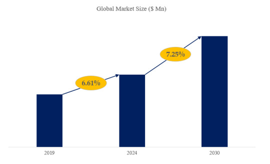
Selon QYResearch, les principaux fabricants mondiaux de Analyseurs de taille de particules par diffusion de lumière statique comprennent Malvern Panalytical, Anton Paar, Dandong Bettersize, HORIBA, Sympatec, FRITSCH GmbH, Omec, Beckman Coulter, Shimadzu, Microtrac MRB, etc. En 2023, les cinq premiers acteurs mondiaux détenaient une part d'environ 68.0% en termes de chiffre d'affaires.
Figure 2. Classement et part de marché des 12 premiers acteurs mondiaux de Analyseurs de taille de particules par diffusion de lumière statique (Le classement est basé sur le chiffre d'affaires de 2023, continuellement mis à jour)

The key market drivers for the Static Light Scattering Particle Size Analyzers market:
1. Increasing Demand for Particle Size Analysis in Various Industries: The growing need for particle size analysis in industries such as pharmaceuticals, chemicals, materials science, and food processing has been a primary driver for the static light scattering particle size analyzers market.
2. Stringent Regulatory Requirements and Quality Control Measures: Regulations and standards governing product quality, safety, and performance in various industries have necessitated the use of precise particle size analysis techniques, including static light scattering.
3. Advancements in Optical and Electronic Technologies: Continuous improvements in optics, electronics, and data processing capabilities have enhanced the performance and accuracy of static light scattering particle size analyzers.
4. Increasing Importance of Particle Characterization in Research and Development: The critical role of particle size analysis in research and development activities across various industries, such as materials science, nanotechnology, and biotechnology, has driven the demand for static light scattering analyzers.
5. Growing Demand for Nano and Micro-Particle Characterization: The increasing focus on the development and application of nanomaterials and micro-particles in diverse industries has fueled the need for advanced particle size analysis techniques like static light scattering.
6. Expansion of the Pharmaceutical and Biotechnology Industries: The growth of the pharmaceutical and biotechnology sectors, where particle size analysis is essential for drug formulation, drug delivery, and quality control, has been a significant driver for the static light scattering particle size analyzers market.
7. Increasing Environmental Regulations and Pollution Monitoring: The rising emphasis on environmental regulations and the need for effective monitoring of airborne and waterborne particulates have contributed to the demand for static light scattering particle size analyzers.
8. Technological Convergence and Integration of Analytical Techniques: The integration of static light scattering with other analytical techniques, such as dynamic light scattering and laser diffraction, has expanded the applications and versatility of particle size analysis.
9. Emerging Applications in Emerging Markets and Developing Economies: The growing adoption of particle size analysis in developing regions, driven by the expansion of various industries and the need for quality control, has presented new opportunities for the static light scattering particle size analyzers market.
À propos de QYResearch
QYResearch a été fondée en 2007 en Californie aux États-Unis. C'est une société de conseil et d'étude de marché de premier plan à l'échelle mondiale. Avec plus de 17 ans d'expérience et une équipe de recherche professionnelle dans différentes villes du monde, QYResearch se concentre sur le conseil en gestion, les services de base de données et de séminaires, le conseil en IPO, la recherche de la chaîne industrielle et la recherche personnalisée. Nous société a pour objectif d’aider nos clients à réussir en leur fournissant un modèle de revenus non linéaire. Nous sommes mondialement reconnus pour notre vaste portefeuille de services, notre bonne citoyenneté d'entreprise et notre fort engagement envers la durabilité. Jusqu'à présent, nous avons coopéré avec plus de 60 000 clients sur les cinq continents. Coopérons et bâtissons ensemble un avenir prometteur et meilleur.
QYResearch est une société de conseil de grande envergure de renommée mondiale. Elle couvre divers segments de marché de la chaîne industrielle de haute technologie, notamment la chaîne industrielle des semi-conducteurs (équipements et pièces de semi-conducteurs, matériaux semi-conducteurs, circuits intégrés, fonderie, emballage et test, dispositifs discrets, capteurs, dispositifs optoélectroniques), la chaîne industrielle photovoltaïque (équipements, cellules, modules, supports de matériaux auxiliaires, onduleurs, terminaux de centrales électriques), la chaîne industrielle des véhicules électriques à énergie nouvelle (batteries et matériaux, pièces automobiles, batteries, moteurs, commande électronique, semi-conducteurs automobiles, etc.), la chaîne industrielle des communications (équipements de système de communication, équipements terminaux, composants électroniques, frontaux RF, modules optiques, 4G/5G/6G, large bande, IoT, économie numérique, IA), la chaîne industrielle des matériaux avancés (matériaux métalliques, polymères, céramiques, nano matériaux, etc.), la chaîne industrielle de fabrication de machines (machines-outils CNC, machines de construction, machines électriques, automatisation 3C, robots industriels, lasers, contrôle industriel, drones), l'alimentation, les boissons et les produits pharmaceutiques, l'équipement médical, l'agriculture, etc.
#Analyseurs de taille de particules par diffusion de lumière statique#Static Light Scattering Particle Size Analyzers
0 notes