#PCB Assemble Factory
Explore tagged Tumblr posts
Visit Tumblr Blog
Explore Tumblr blogs with no restrictions, modern design and the best experience.
Last Seen Tumblr Blogs


Fun Fact
Users from the US are the majority of Tumblr visitors.
Text
What is PCB Assembly ?
PCB Assembly manufacturer - Hitech Circuits Co., Limited
It’s the step in the manufacturing process in which you populate a blank board with the electronic components needed to make it into a functional printed circuit board. It’s these components that make a board into the circuit that enables an electronic product to function. PCB assembly typically takes place via one of two processes:
1. Surface-mount technology
SMT: SMT stands for “Surface Mount Technology“. The SMT components are very small sizes and comes in various packages like 0201, 0402, 0603, 1608 packages for resistors and capacitors. Similarly for Integrated circuits ICs we have SOIC, TSSOP, QFP and BGA.
The SMT components assembly is very difficult for human hands and can be time taking process so it is mostly done by automated pick and place machine.
2. Through-hole manufacturing
THT: THT stands for “Through hole Technology”. The components with leads and wires, like resistors, capacitors, inductors, PDIP ICs, transformers, transistors, IGBTs, MOSFETS are example.
The component has to be inserted on one side of PCB and pulled by leg on other side and cut the leg and solder it. The THT components assembly is usually done by hand soldering and is relatively easy.
Printed Circuit Board Assembly Techniques
There are only two common PCBA techniques available for use by a PCB designer. The methods are:
1. Automated PCB Assembly Techniques
Generally, this technique employs the use of state of the art machines, which are fully automatic. For example, the surface mount components are worth positioning with the aid of an automated pick and place machine.
Again, reflow soldering is commonly for surface mount components usually done in a reflow oven. An automated solder stencil is also used to apply the solder paste on the PCB.
Finally, high tech inspection machines are used to confirm and check the quality of the PCBA. Some of which include: Automated optical inspection machine (AOI), X-ray inspection machines, etc.
Above all, due to the precise monitoring, control of soldering, no human input and versatile machines.
This technique ensures utmost efficiency, output consistencies, and limits defects.
2. Manual PCB Assembly Techniques
This method is favorite for use with through-hole parts, which needs manual placement on the board. Besides, with these through-hole parts, it’s advisable you use wave soldering. Note that in the through- hole assembly process, you need to place the components and electronics on the PCB.
After that, you use wave soldering to solder the leads. Typically, you will need an individual to insert a component into a marked PTH. Once done, transfer the PCB to the next station where the next person will be on standby tasked with fixing another part.
What are the Benefits of SMT PCB Assembly?
SMT assembly provides many benefits and some of them are as follows:
It can be used to incorporate small components.
In SMT, the components can be placed on both sides of the board.
It assures high component densities.
Fewer holes need to be drilled for surface mounting than through-hole.
It require low initial costs and time for setting up the mass production.
SMT is the simpler and faster-automated assembly when compared to through-hole.
Errors regarding the component placement can be easily rectified.
Surface mount PCBs feature strong joints, which can easily withstand vibrations.
What are the techniques used in Surface Mount Technology?
There are several techniques for the reflow process. After applying the solder paste or a flux mixture on the board and after placing the components, the boards are conveyed to a reflow soldering oven. The techniques used for reflowing soldering include infrared lamps, hot gas convection, fluorocarbon liquids with a high boiling point, and so on.
What are the different testing methods used in SMT PCB Assembly?
Hitech Circuits as the PCB assembly manufacturer, we perform the following testing and inspection to ensure the quality of surface mount PCBs.
Automated Optical Inspection (AOI): This is performed before and after the soldering to identify the component placement, presence, and solder quality.
X-ray Testing: In this type of testing, the operator relies on the X-ray images of the PCB to check the solder joints and lead-less components such as Quad Flat Packs and ball grid arrays, which are generally not visible to naked eyes.
In-Circuit Testing (ICT): This method is used to detect manufacturing defects by testing the electrical properties in the SMT Assembly.
What type of files or documents should I send for SMT PCB Assembly?
Gerber Files: The file contains all details of physical board layers including solder masks, copper layers, drill data, legends, and so on.
Bill of Materials (BOM): This contains information on the list of items needed for the PCB manufacturing and the instructions of manufacturing.
Pick and Place File: This file contains information on all components to be used in the PCB design and their rotation and X-Y coordinates.
The whole process of PCB Assembly
1. Bare board loader machine
The first step in the PCB assembly is to arrange the bare boards on the rack, and the machine will automatically send the boards one by one into the SMT assembly line.
2. Printing solder paste
When PCB on the SMT production line, firstly, we have to print solder paste on it, and the solder paste will be printed on the pads of the PCB. These solder pastes will be melt and solder the electronic parts to the circuit board when it passes through the high-temperature reflow oven.
In addition, when testing new products, some people will use film board/adhesive cardboard instead of solder paste, which can increase the efficiency for adjusting the SMT machines.
3. Solder paste inspection machine(SPI)
Since the quality of solder paste printing is related to the quality of welding of subsequent parts, some SMT factories will use optical machine to check the quality of solder paste after printed the solder paste in order to ensure stable quality. If there any poorly printed solder paste board, we will wash off the solder paste on it and reprint, or remove the excess solder paste if there is redundant solder paste on it.
4. High speed SMT machine
Usually, we will put some small electronic parts (such as small resistors, capacitors, and inductors) to be printed on the circuit board first, and these parts will be slightly stuck by the solder paste just printed on the circuit board, so even if the speed of printing is very fast and the parts on the board will not fall away. But large parts are not suitable for use in such high speed SMT machines, which will slow down the speed of small parts assembly. And the parts will be shifted from the original position due to the rapid movement of the board.
5. Universal SMT machine
Universal SMT machine is also known as "slow machine", it will be assembled some large electronic components, such as BGA IC, connectors, etc., these parts need more accurate positions, so the alignment is very important. Use a camera to take a picture to confirm the position of the parts, so the speed is much slower than High speed SMT machine we taked before. Due to the size of the components here, not all of them are packed in tape and reel, and some may be packed in trays or tubes. But if you want the SMT machine to recognize the trays or tube-shaped packaging materials, you must configure an additional machine.
Generally, traditional SMT machines are using the principle of suction to move electronic parts, and in order to place the parts successfully, and there must be the flat surface on these electronic components for the suction nozzle of the SMT machine to absorb. However, for some electronic parts don’t have a flat surface for these machines, and it is necessary to order special nozzles for these special-shaped parts, or add a flat tape on the parts, or wear a flat cap for thees electronic parts.
6. Manual parts or visual inspection
After assembled all parts by the high speed SMT machine or Universal SMT machine and before going through the high-temperature reflow oven, and we will set up a visual inspection station here and to pick out the deviation parts or missing components boards etc., because we have to use a soldering iron to repair if there are still defectives boards after passing the high-temperature oven, which will affect the quality of the product and will also increase the cost. in addition, for some larger electronic parts or traditional DIP parts or some special reasons cannot be processed by the SMT machine before, they will be manually placed on pcb here.
7. Reflow oven
The purpose of reflow oven is to melt the solder paste and form a non-metallic compound on the component feet and the circuit board, that means to solder electronic components on the circuit board. The temperature rise and fall curves often affect the soldering quality of the entire circuit board. According to the characteristics of the solder materials, usually the reflow oven will set the preheating zone, soaking zone, reflow zone, and cooling zone to achieve the best soldering effect.
For example, the melting point for SAC305 solder paste with lead-free is about 217°C, which means that the temperature of the reflow oven must be higher than the melting points to remelt the solder paste. What's more, the maximum temperature in the reflow furnace should not exceed 250°C, otherwise many parts will be deformed or melted because they cannot withstand such a high temperature.
Basically, after the pcb passed through the reflow oven, the assembly for the entire circuit board is almost complete. If there are hand-soldered parts, we need to transfer to DIP process, and then we have to check the quality after reflow oven by QC department.
8. Automatic optical inspection(AOI)
The main purpose of setting up AOI is because some high density boards can’t be process the following ICT test, so we used AOI inspection to replace it. But even using AOI inspections, there still have the blind spots for such checking, for example, the solder pads under the components cannot be checked by AOI. At present, it can only check whether the parts have side standing issue, missing parts, displacement, polarity direction, solder bridges, lack of soldering etc., but cannot checking the BGA solderability, resistance value, capacitance value, inductance value and other components quality, so far AOI inspection can’t completely replace ICT test.
Therefore, there is still some risk if only AOI inspection is used to replace ICT testing, but ICT test is also not 100% make sure the good quality, we suggest these two ways can be combined with together to make sure the good quality.
9. PCB unloader machine
After the board is fully assembled, it will be retracted to the unloder machine, which has been designed to allow the SMT machine to automatically pick and place the board without damaging the quality for PCB.
10. Visual inspection for finished products
Normally there will be a visual inspection area in our SMT production line whether there is an AOI station or not, and it will help to check if there are any defectives after completed assembled the pcbs. If there is an AOI station, it can reduce the visual inspection worker on our SMT line, and to reduce the potential cost, and because it is still necessary to check some places that cannot be judged by AOI, many SMT factories will provide the mainly visual inspection templates at this station, which is convenient for visual inspection worker to inspect some key parts and polarity for components.
11. DIP process
DIP process is a very important process in the whole PCBA processing, and the processing quality will directly affect the functional for PCBA boards, so it is necessary to pay more attention to the DIP process. There are many preliminary preparations for DIP process. The basic process is to re-process the electronic components first, like to cut the extra pins for some DIP components, our staff received the components according to the BOM list, and will check whether the material part numbers and specifications are correct or not, and performs pre-production pre-processing according to the PCBA samples. The steps are: Use various related equipment (automatic capacitor pins cutting machine, jumper bending machine, diode and triode automatic forming machine, automatic belt forming machine and other machines) for processing.

12. ICT test
Printed Circuit board open/short circuit test (ICT, In-Circuit Test), The purpose of ICT test is mainly to test whether the components and circuits on the printed circuit board are open or short issues. It can also measure the basic characteristics of most components, such as resistance, capacitance, and inductance values to judge whether the functions of these parts are damaged, wrong parts or missing parts etc. after passing through the high-temperature reflow oven.
ICT test machines are divided into advanced and basic machines. The basic ICT test machines are generally called MDA (Manufacturing Defect Analyzer). It’s just to measure the basic characteristics of electronic components and judge open and short circuits issue we talked above.
In addition to all the functions of the basic ICT test machines, for advanced ICT test machine can also test the whole PCBA by using power, start to testing the PCBA boards by setting the program in the test machine. The advantage is that it can simulate the function of the printed circuit board under the actual power-on condition, this test can partly replace the following functional test machine (Function Test). But the cost for the test fixture of this advanced ICT test can probably buy a car, it’s too expensive and we suggest it can be used in mass production products.
13. PCBA function test
Functional testing is to make up for the ICT test, because ICT only tests the open and short circuits on the the PCBA board, and other functions such as BGA and other fuctions are not tested, so it is necessary to use a functional testing machine to test all functions on the whole PCBA board.
14. Cutting board (assembly board de-panel)
Normally, printed circuit boards will be produced in panel, and it will be assembled to increase the efficiency of SMT production. It means several single boards in one panel, such as two-in-one, four-in-one etc. After finished all the pcb assembly process, it needs to be cut into single boards, and for some printed circuit boards with only single boards also need to cut off some redundant board edges.
There are several ways to cut the printed circuit board. You can design the V-cut using the blade cutting machine (Scoring) or directly manually break off the board (not recommended). For more high density circuit boards, it will be used the professional splitting machine or the router to split the board without any damage the electronic components and printed circuit boards, but the cost and working hours will be a little longer.
Why Choose Hitech Circuits PCB Assembly Manufacturer for Your PCB Assembly Projects?
There are several PCB manufacturers specializing in PCB assemblyservices. However, Hitech Circuits PCB Assembly stands out owing to the following:
Assistance in Material Procurement:
Technically, in PCB assembly services, the quality of parts is the responsibility of the OEM; however, we ease your job by assisting you to make the right selection. We can help you procure all your parts of the same type own a single part number, thanks to our supply chain and vendor network as well as experience. This saves time and cost that goes in ordering single parts as you plan.
Testing procedures:
We are very focused on quality and thus implement stringent testing procedures at each stage of the assembly and after completion.
Fast Turnaround Times:
Our well-equipped facility and the right tools enable us to complete your requirements well before time, and without compromising on the quality or functioning of the PCBs. For simple designs we revert in 24 to 48 hours.
Cost Effectiveness:
While PCB assembly is a cost-effective alternative, we go a step further and assure that the parts you list are of a good quality and suitable for your requirement. Also, you can control the part flow and replenish them as needed. This eliminates the need to buy extra stock and store it.
Quick Quote:
We offer a quick quote based on your BOM. All you need is a detailed BOM, Gerber files, your application requirement sheet, and quantity.
We’re not one to stand still, which is why we use the latest equipment and the finest minds to create your PCB projects. We’re constantly keeping our finger on the pulse of the latest trends. And as a result, we know how to deliver the highest standards of PCB assembly to meet all your requirements.
Our dedicated, friendly customer service team also means that we support you every step of the way. Offering our expert guidance to ensure a complete PCB project that you’re happy with.
Contact us today
No matter what your printed circuit board assemblyneeds are, we always aim to deliver efficient, dependable solutions. For more information about our services, do not hesitate to get in touch with us today for a no-obligation quote
2 notes
·
View notes
Text
High-Quality PCB Production for Accuracy and Performance
We specialize in PCB production at the highest level of the industry at ESPCBA. Through prototype to mass production, our cutting-edge technology provides accuracy, reliability, and quick turnaround. With the trust of our international clients, we provide customized PCB solutions that are made to order for you. Find out why ESPCBA is the most trusted and efficient PCB producer visit us today at espcba.
Read More : https://espcba.com/how-to-choose-the-right-pcb-assembly-factory-for-your-electronics-business/
0 notes
Text

Serviço de fabricação de PCB de alta frequência e PCB de alta velocidade
PCB de alta frequência
As placas de circuito impresso são muito procuradas porque tornam o circuito compacto durável e garantem um desempenho ideal com poucos erros e mau funcionamento. Atualmente, existem diferentes tipos de PCBs disponíveis que podem ser usados em qualquer lugar, até mesmo em uma pequena lanterna ou em uma grande nave espacial. Um dos tipos especiais de PCB é a PCB de alta frequência, que é usada para fins especiais. Ela facilitou muitas coisas que não eram possíveis de serem feitas com uma PCB normal.

O que é PCB de alta frequência?
Uma PCB de alta frequência se refere a uma PCB especial que tem uma faixa de frequência de 500 MHz a 2 GHz. Essa é uma faixa de frequência muito alta que não pode ser alcançada em PCBs padrão, e é por isso que essas PCBs são usadas para fins específicos em que os sinais de alta frequência são transmitidos. A PCB de alta frequência é uma placa de circuito produzida em uma placa revestida de cobre com substrato de micro-ondas usando parte dos métodos comuns de fabricação de placas de circuito rígido ou usando métodos de processamento exclusivos. Devido à alta frequência, a comunicação e a transmissão de sinais são realizadas em um ritmo mais rápido. O principal uso das PCBs de alta frequência é em comunicações sem fio, incluindo satélites, telecomunicações e sistemas de radar.
Por que PCB de alta frequência?
Quando se trata de transmitir um sinal em uma frequência mais alta, há muitas chances de perdas, atrasos e distorções no sinal. Portanto, se usarmos uma placa de circuito impresso padrão para fins de alta velocidade ou alta frequência, os resultados não serão os melhores. Os sinais podem se perder ou pode haver grandes perdas após o recebimento do sinal.
Além disso, não podemos eliminar o uso de sinais de alta frequência no circuito porque esse é o futuro. Atualmente, a transmissão sem fio é muito difundida, e o melhor exemplo é um roteador Wi-Fi que funciona em sua casa. Alguns componentes e switches complexos precisam de sinais mais rápidos, portanto, o sinal tem uma frequência mais alta. Em palavras simples, os aplicativos de alta frequência estão aumentando a cada dia devido às vantagens que eles oferecem. Portanto, não há outra opção a não ser optar por sinais de baixa frequência para evitar o problema.
A única solução para esses problemas é a PCB de alta frequência. Uma placa de circuito impresso de alta frequência é feita de materiais exclusivos e tem algumas características específicas que lhe permitem transferir sinais de alta frequência com perda mínima. A placa de circuito impresso de alta frequência é ideal para aplicações de alta velocidade.

Materiais para PCB de alta frequência
Os materiais usados para PCBs de alta frequência têm qualidades exclusivas. Se o material escolhido estiver correto, ele oferecerá os melhores resultados. Antes de selecionar qualquer material, você precisa examinar algumas especificações para saber se o material é adequado para a aplicação ou não.
Os fatores importantes que você precisa observar são:
Constante dielétrica (DK)
Fator de dissipação (DF)
Coeficiente de expansão térmica
Absorção de umidade
Nós Hitech Circuits estamos sempre dedicados a fornecer preços competitivos, boa qualidade e prazo de entrega rápido para nossos clientes. Se você tiver alguma necessidade de PCI, não hesite em contactar-me.
#high frequency pcb#PCB#PCBA#assembly#PCB manufacturer#PCB factory#PCB China#Hitech Circuits#Hitech PCB
1 note
·
View note
Text
China Cable Wire Harness Assembly: Why Topscom Technology is Your Best Choice
In today's fast-paced technological world, cable wire harness assemblies play a crucial role in various industries, from automotive and aerospace to consumer electronics and industrial machinery. These assemblies ensure efficient power transmission, signal connectivity, and overall system reliability. For companies looking to source high-quality cable wire harness assemblies, China has become a prominent global hub due to its advanced manufacturing capabilities and competitive pricing. Among the many providers in China, Topscom Technology stands out as a leading choice for superior China cable wire harness assembly services. https://is.gd/RIk8ag
PCB SMT assembly, China printed circuit board assembly, China PCB factory, China PCB fabrication, China PCB manufacturing, China PCB board, China PCB manufacturer, China PCB service, China PCB prototype, China PCB supplier, China PCB, PCB China, China PCB online, PCB board, China PCB assembly, PCBA China, China PCB design, PCB assembly, China PCB quote, PCBA, contract manufacturing China, China contract manufacturing, contract manufacturing, China electronic assembly, China electronic manufacturing, electronics manufacturing, electronic board manufacturers, China OEM manufacturing, OEM manufacturing, China cable wire harness assembly

0 notes
Text

As a top China PCB manufacturer, Hitech Circuits has a lot of experience and skill in every part of PCB production, from layout and design to manufacturing, testing, and after-sales support. All our work is done in our ISO-certified factory, ensuring high quality at every step. We focus on excellence, with each circuit board going through strict quality control before delivery. We make a wide range of printed circuit boards, including PCB prototypes, FR4 PCB, double-sided PCB, aluminum PCB, RF PCB, ceramic PCB, high-frequency PCB, and HDI PCB. If you need a reliable PCB manufacturer in China, contact us today! Just send email to [email protected] . For more information, please visit https://hitechcircuits.com/
#pcb manufacturer#pcb assembly#ceramic pcb#hdi pcb#PCB prototypes#fr4 pcb#double-sided PCB#multilayer pcb#aluminum PCB#pcb factory#pcb fabrication#RF PCB#high frequency
0 notes
Text
PCB Factories And PCB Assembly In China: A Comprehensive Insight
In the realm of modern electronics, printed circuit boards (PCBs) are the backbone, connecting and supporting the electronic components that drive the devices we use daily. As technology advances and the demand for sophisticated electronics grows, the importance of efficient and reliable PCB manufacturing and assembly has never been greater. China, in particular, has emerged as a global leader in this industry. This article delves into the reasons behind China's dominance in PCB factory and PCB assembly, highlighting the factors that contribute to its success and what it means for the global electronics market.
0 notes
Text
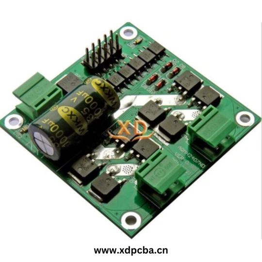
XDPCBA.cn stands at the forefront of PCBA board manufacture, delivering excellence through precision engineering and cutting-edge technology. Our state-of-the-art facilities and skilled professionals ensure the highest quality in every PCBA board we manufacture. With a focus on reliability and innovation, XDPCBA.cn is your trusted partner for customized PCBA solutions. Experience seamless integration, superior performance, and unmatched expertise when you choose XDPCBA.cn for your PCBA board manufacturing needs. Explore a new level of electronic precision with us.
Read More : https://www.xdPCBA.cn/5228367151253673.html
0 notes
Text
#smart watch assembly#smart watch factory#smart wearable tws assembly#cable wiring harness factory#quality Smart Watch Assembly#affordable Smart Watch Assembly#best Smart Watch Factory#electronics pcba factory#printed circuit board assembly#electronics#smt pcb jobwork#electronics manufacturer
0 notes
Text
hi,I'm zoe,a sales engineer in the Shenzhen STHL Electronics Co.,Ltd.we are a professional PCB & PCBA manufacturing servicer with more than 18 years of experience located in Shenzhen, China. Mainly provide services of electronic components sourcing + PCB fabrication + PCB Assembly + Housing assembly + Function testing services.
Our factory covers 7000+ square meters, has 5 (Panasonic) high-speed SMT production lines, 2 DIP lines, 2 testing lines, and 180+ workers, passed ISO9001, ISO14001, ISO13485 and IATF 16949 certifications, win recognization by Littelfuse, Hisense,Surfilter, etc.
2 notes
·
View notes
Text


Printed circuit board manufacturing which is our major business, I think you already know, we are a PCB manufacturer. We have 3 branch factories dedicated to Quick Turn PCB Prototypes Manufacturing, Small and Medium-volume Printed Circuit Board, FPC Manufacturing services and PCB assembly services. Our market target is the High Multilayer PCB, High Density PCB, Flexible PCB, Rigid-flex PCB, Heavy copper PCB, Rogers PCB, Ceramic PCB and Special Materials Printed Circuit Boards.
Also, we can help customer sourcing components, wire PCB assembly and provide one-stop service.
Hitech Group is capable of providing full turn-key and partial turn-key PCB assembly services. For full turn-key, we take care of the entire process, including manufacture of Printed Circuit Boards, procurement of components, order tracking, continuous monitoring of quality and final board assembly. Whereas for partial turn-key, the customer can provide the PCBs and certain components, and the remaining parts will be handled by us.
4 notes
·
View notes
Text
PCB Assembly & Electronic Assembly service & electronics manufacturing company – Hitech Circuits Co., Limited As leading one-stop PCB Assembly services provider in China, Hitech Group offers high quality, cost effective and express PCB board products and provides PCB manufacturing, electronics assembly manufacturing, components sourcing, Box build assembly and PCBA testing services for our customers. [email protected] www.hitechcircuits.com
#pcba manufacturing#pcb manufacturer#pcb assembly#flex pcb#pcb fabrication#pcb#pcb factory#smt assembly#flexible circuit board
0 notes
Text
Reliable PCB Factory for High-Quality Circuit Board Production
Searching for a trusted PCB factory? ESPCBA offers high-quality printed circuit board production with accuracy, speed, and reliability you can count on. From prototype to mass production, we offer cutting-edge PCB solutions that meet your requirements. Check out our services at https://espcba.com/ and collaborate with a PCB factory that's dedicated to excellence, innovation, and quick turnaround for each order.
Read More : https://espcba.com/fast-reliable-pcb-assembly-why-oems-and-electronics-manufacturers-trust-espcba/
0 notes
Text
Turnkey Electronics Contract Manufacturing Services, PCB Assembly Services - Topscom
Topscom helps manufacturers of low to medium volume and high volume, high complexity Electronics products focus on the core activities that deliver value to them. We provide complete outsourced manufacturing solutions, provides customers with complete engineering, testing services, and manufacturing resources that are vertically integrated with components to optimize their operations by lowering their costs and reducing their time to markets. https://is.gd/nL4r0T
PCB SMT assembly, China printed circuit board assembly, China PCB factory, China PCB fabrication, China PCB manufacturing, China PCB board, China PCB manufacturer, China PCB service, China PCB prototype, China PCB supplier, China PCB, PCB China, China PCB online, PCB board, China PCB assembly, PCBA China, China PCB design, PCB assembly, China PCB quote, PCBA, contract manufacturing China, China contract manufacturing, contract manufacturing, China electronic assembly, China electronic manufacturing, electronics manufacturing, electronic board manufacturers, China OEM manufacturing, OEM manufacturing, China cable wire harness assembly

0 notes
Text
Comprehensive Guide to PCB Board Design & Printed Circuit Assembly for Optimal Electronic Performanc
Compre
Modern electronics rely heavily on printed circuit boards (PCBs). Without well-designed PCBs and quality assembly, devices can become unreliable or fail prematurely. Whether you’re a designer or manufacturer, understanding how to create and assemble high-quality PCBs is crucial. This guide covers essential design principles, manufacturing methods, testing, and tips for better PCB performance.
Understanding PCB Board Design Fundamentals
The Role of PCB Design in Electronics Functionality
PCB design is the blueprint that shapes how your device works. It directly influences electrical signals, heat management, and overall durability. Poor design can lead to issues like signal interference or overheating, hurting the product's performance. Good design results in a more reliable, longer-lasting device that customers can count on.
Essential Components of a PCB Design
A PCB isn’t just a green board with some wires. It includes multiple elements such as:
Layers: These are the different sheets of the PCB, repeating signals or power.
Traces: Thin lines of copper that connect components.
Pads: Contact points for mounting parts like chips or resistors.
Vias: Small holes that link traces on different layers.
Components: Resistors, capacitors, ICs, and other parts attached to the board.
Each piece affects how well the circuit functions. Proper layout and placement ensure electrical signals flow smoothly and the device functions as intended.
Designing for Manufacturing (DFM) Best Practices
Designing with manufacturing in mind helps lower costs and speeds up production. Here are key tips:
Use standard component sizes and footprints.
Keep traces wide enough to handle current.
Avoid tiny vias or complex shapes that are hard to manufacture.
Place components logically to reduce assembly time.
Minimize the number of layers if possible. Fewer layers often mean lower costs.
These practices make it easier for factories to produce your design without errors or delays.
Types of Printed Circuit Boards and Their Applications
Rigid PCBs
Rigid PCBs are the most common type. They’re made of solid material, like fiberglass, that keeps the board stiff. You’ll find these in everything from computers to appliances. They’re reliable, cost-effective, and easy to handle during assembly.
Flexible and Rigid-Flex PCBs
Flexible PCBs bend and fold, fitting into small spaces inside devices. Rigid-flex combines both types, offering stiffness where needed and flexibility elsewhere. These are popular in wearable tech and smartphones, where space is tight.
High-Frequency and HDI PCBs
Special boards designed for fast signals — known as high-frequency PCBs — are used in radio, radar, and satellite systems. HDI (High-Density Interconnect) PCBs pack more components into less space, ideal for miniaturized electronics like medical devices or smartphones.
The Printed Circuit Assembly (PCA) Process
From Design to Production: Step-by-Step Overview
A typical PCA process includes:
Designing the circuit using CAD tools.
Verifying the design for errors.
Creating prototypes for testing.
Moving into full-scale manufacturing.
Assembling components via soldering.
At every step, quality checks are essential to prevent costly mistakes later.
Key Manufacturing Techniques
Surface-Mount Technology (SMT): Attaching components on the surface. It’s fast and suitable for high-volume production.
Through-Hole Assembly: Inserting pins into drilled holes. Best for parts needing full mechanical strength.
Automated Assembly: Robots place components quickly with high precision.
Manual Assembly: Used for small runs or complex parts, but slower.
Choosing the right method impacts the speed and quality of your PCB production.
Quality Control and Inspection
Regular inspections catch problems early:
X-ray Inspection: Checks hidden solder joints.
Automated Optical Inspection (AOI): Finds defects on the surface.
SPI (Solder Paste Inspection): Ensures correct solder paste volume.
Complying with standards like IPC-610 and IPC-2221 helps keep quality high and consistent.
Critical Factors Influencing PCB and PCA Quality
Material Selection for Durability and Performance
Choosing the right materials makes a difference:
Substrates like FR-4 are common but vary in quality.
Copper thickness affects current capacity.
Solder masks prevent shorts and corrosion.
Durable materials stand up to temperature, vibration, and environmental stress.
Design for Reliability
To keep your device working long-term:
Minimize electrical interference by proper grounding.
Manage heat by placing heat-sensitive parts away from heat sources.
Use clear labels and ample space for easy assembly and maintenance.
Good practice prevents failure and reduces warranty repairs.
Environmental Considerations
PCBs face many conditions:
Use conformal coatings to protect from moisture.
Choose vibration-resistant designs for mobile devices.
Select temperature-tolerant materials for harsh environments.
Designing for these factors enhances lifespan and performance.
Cost Optimization
Balancing quality with budget is key:
Use standard components rather than custom parts.
Avoid overly complex designs.
Optimize layout for easy assembly.
Good planning reduces waste and keeps costs in check.
Best Practices for PCB Design and Assembly Optimization
Design Tips for Ease of Assembly
Properly space components for automatic placement.
Use clear silkscreen labels to identify parts.
Keep copper traces away from component pads for easier soldering.
Simplicity saves time during manufacturing and reduces errors.
Enhancing Manufacturing Efficiency
Stick to standard footprints.
Avoid intricate shapes on copper traces.
Use consistent pad sizes and pad-to-component spacing.
This approach speeds up production and keeps quality high.
Post-Assembly Testing and Validation
Once assembled, testing is crucial:
Conduct functional testing to verify operation.
Use burn-in tests to detect early failures.
Carry out long-term stress tests for durability.
Thorough testing ensures your product withstands real-world use.
Collaborating with Proven PCB Manufacturers
Choose manufacturers with:
Certifications like IPC-6012 or ISO 9001.
Experience in your specific PCB type.
Good communication and ability to meet deadlines.
Partnering with reliable suppliers reduces risks and improves final product quality.
Case Studies and Real-World Examples
Some companies have achieved great results by focusing on PCB design. For example, an electronics firm reduced their device failure rate by improving trace routing and component placement. Conversely, poor design choices, such as crowded traces, led to short circuits and costly recalls. Learning from these stories highlights the importance of meticulous planning and quality control.
Conclusion
Creating a high-performance PCB, from design to assembly, is essential for reliable electronics. Focus on good design practices, choose the right materials, and work with experienced manufacturers. Regular testing and inspection help catch issues before products hit the market. As technology advances, keep an eye on trends like miniaturization and high-frequency PCBs. Staying current ensures your designs remain competitive and durable. Quality now means better devices, happier users, and fewer headaches later.
0 notes
Text
What Makes PCB Factory and PCB Assembly China a Strategic Choice?
Understanding the nuances of PCB manufacturing and PCB assembly China is key to making informed decisions for your electronic projects. By opting for accredited factories, navigating the assembly process with precision, exploring cost-effective solutions, and incorporating strategic prototyping, you position your projects for success in the dynamic world of electronics.
0 notes
Text
Decoding PCBA Board Manufacture: A Roadmap to Efficient Production

PCBA (Printed Circuit Board Assembly) board manufacture stands as a pivotal stage in the journey from electronic concept to tangible product. This blog offers a detailed roadmap, guiding both novices and seasoned professionals through the multifaceted process of PCBA board manufacture.
The journey initiates with an elucidation of PCBA board components, ranging from basic resistors to intricate microprocessors. Understanding the role and compatibility of each component is paramount in crafting a functional and efficient board.
Subsequently, the blog navigates through the intricacies of PCB fabrication, encompassing design optimization, material selection, and fabrication techniques. Through insights into surface finishes, layer stackups, and trace routing, readers will grasp the fundamentals necessary for creating robust and reliable PCBs.
The narrative then transitions to the assembly phase, shedding light on component placement, soldering methodologies, and quality assurance protocols. From manual soldering to automated pick-and-place systems, readers will gain insight into the diverse assembly techniques and their respective advantages.
Moreover, the blog addresses the significance of thorough testing and inspection procedures to identify and rectify potential defects before the final product reaches the market. Topics such as in-circuit testing, functional testing, and quality control standards underscore the importance of delivering reliable and high-performance PCBAs.
In conclusion, "Decoding PCBA Board Manufacture" serves as a comprehensive guide for navigating the complexities of PCB assembly manufacturing. By leveraging the insights and best practices shared in this blog, electronics enthusiasts and industry professionals alike can streamline their manufacturing processes, ultimately fostering innovation and excellence in the realm of electronic design and production.
#pcb circuit#fr4 pcb#pcb factory#circuit board#led circuit board#flex pcb#pcb assembly#aluminum pcb#fpc#ems pcba
0 notes