#PCB manufacturer
Text
PCB Manufacturing-PCB Assembly-Hitech Circuits
Hitech Circuits is a lеаding PCB Manufacturing & PCB Assembly company with more than 20 years experience in the electronics manufacturing industry. We focus on PCB Design, PCB Layout, Circuit board fabrication, Turnkey PCB assembly, and electronic parts sourcing services.
With mature supply chain, talented design team, advanced manufacturing techniques and quality control systems, Hitech is able to provide one-stop electronics manufacturing services and solution for our customers to help them stand out in the marketplace.
We offer a full range of Electronic manufacturing services.
-LED PCB
-Heavy Copper PCB
-Multilayer PCB
-HDI PCB
-Flexible PCB
-Rigid-Flex PCB
-High Speed PCB
-High Frequency PCB
-PCB Reverse Engineering
7 notes
·
View notes
Text
The Benefits of Ordering Printed Circuit Boards Online: A Guide to Choosing the Right PCB Manufacturer
In today's rapidly advancing technological landscape, printed circuit boards (PCBs) play a crucial role in various electronic devices, from smartphones to industrial machinery. As demand for these essential components grows, businesses and hobbyists alike seek efficient and cost-effective solutions for obtaining high-quality PCBs. One of the most convenient methods is to order printed circuit boards online. In this article, we will explore the advantages of ordering PCBs online and provide insights into selecting a reputable PCB manufacturer.
Why Order Printed Circuit Boards Online?
Ordering printed circuit boards online offers several benefits, making it an attractive option for many businesses and individuals:
Convenience: The ability to order PCBs from the comfort of your home or office eliminates the need for in-person visits to manufacturers or suppliers. This convenience saves time and effort, allowing you to focus on your projects or business operations.
Wide Range of Options: Online PCB manufacturers offer a variety of options in terms of materials, layer counts, finishes, and more. This flexibility allows you to customize your PCBs according to your specific requirements and budget.
Cost-Effectiveness: Many online PCB manufacturers provide competitive pricing, especially for bulk orders. Additionally, you can easily compare prices and services from different providers, ensuring you get the best value for your money.
Quick Turnaround Times: Online ordering often comes with expedited production and shipping options, allowing you to receive your PCBs faster. This is particularly beneficial for projects with tight deadlines or when you need quick prototypes.
Access to Advanced Technologies: Many online PCB manufacturers offer advanced technologies such as high-frequency PCBs, flexible PCBs, and more. This access to cutting-edge technology ensures your designs are compatible with the latest industry standards.
Choosing the Right PCB Manufacturer
Selecting the right PCB manufacturer is crucial to ensuring the quality and reliability of your printed circuit boards. Here are some key factors to consider when choosing a PCB manufacturer:
Experience and Reputation: Look for a manufacturer with a solid track record and positive reviews from previous customers. Experienced manufacturers are more likely to produce high-quality PCBs and provide reliable service.
Quality Assurance: Ensure the manufacturer follows strict quality control measures, such as ISO certification and regular testing. High-quality PCBs are essential for the proper functioning and longevity of your electronic devices.
Customer Support: Good customer support is vital, especially if you encounter issues during the ordering process or with the final product. Choose a manufacturer that offers responsive and helpful customer service.
Manufacturing Capabilities: Check the manufacturer’s capabilities, including the types of PCBs they can produce, their layer count capacity, and the materials they use. Make sure they can meet your specific design requirements.
Lead Times and Shipping: Consider the manufacturer’s production lead times and shipping options. Quick turnaround times are crucial for meeting project deadlines, so choose a manufacturer that can deliver within your required timeframe.
Pricing and Payment Terms: While cost is an important factor, it should not be the sole consideration. Ensure the manufacturer offers transparent pricing and flexible payment terms that suit your budget.
Conclusion
Ordering printed circuit boards online is a convenient and cost-effective way to obtain high-quality PCBs for your projects. By choosing a reputable PCB manufacturer, you can ensure the reliability and performance of your electronic devices. Whether you are a business looking to streamline your supply chain or a hobbyist working on a personal project, ordering PCBs online provides a seamless and efficient solution.
For those ready to place a printed circuit board order online, consider the factors outlined above to select the right PCB manufacturer for your needs. With the right partner, you can bring your electronic designs to life with precision and quality.
#printed circuit board#pcb manufacturer#pcb supplier#printed circuit board order online#pcb design & manufacturing services#pcb circuit manufacturer in ahmedabad#electronic circuit design company
2 notes
·
View notes
Text

#pcb#pcba#pcbassembly#pcb manufacturer#pcb board#pcb factory#pcb fabrication#aluminum pcb#pcb design#pcb prototype
2 notes
·
View notes
Text
PCB schematic/design/fabrication/assembly
MPN TECH Pte Ltd provides One-Stop PCBA Solutions in Singapore, which support from R&D prototype to mass production. We have built long-term collaborations with many local startups, SIMES, MNCS, etc. We also have lots of overseas PCBA projects in Europe and the US. If any questions feel free to let me know.
Our Solutions:
PCB Design;
PCB Fabrication;
Components souring;
PCB Assembly;(SG Local machine Assembly)
3 notes
·
View notes
Text

Fine Trak System is one of the leading printed circuit board manufacturers & exporters in the world with our manufacturing unit spread across 5000 sq. mt. We are one of the best companies that are involved in the manufacturing of Printed Circuit Boards. We are highly recognized for providing the best quality Printed circuit boards at a highly effective price.
2 notes
·
View notes
Text
What is PCB Assembly ?
PCB Assembly manufacturer - Hitech Circuits Co., Limited
It’s the step in the manufacturing process in which you populate a blank board with the electronic components needed to make it into a functional printed circuit board. It’s these components that make a board into the circuit that enables an electronic product to function. PCB assembly typically takes place via one of two processes:
1. Surface-mount technology
SMT: SMT stands for “Surface Mount Technology“. The SMT components are very small sizes and comes in various packages like 0201, 0402, 0603, 1608 packages for resistors and capacitors. Similarly for Integrated circuits ICs we have SOIC, TSSOP, QFP and BGA.
The SMT components assembly is very difficult for human hands and can be time taking process so it is mostly done by automated pick and place machine.
2. Through-hole manufacturing
THT: THT stands for “Through hole Technology”. The components with leads and wires, like resistors, capacitors, inductors, PDIP ICs, transformers, transistors, IGBTs, MOSFETS are example.
The component has to be inserted on one side of PCB and pulled by leg on other side and cut the leg and solder it. The THT components assembly is usually done by hand soldering and is relatively easy.
Printed Circuit Board Assembly Techniques
There are only two common PCBA techniques available for use by a PCB designer. The methods are:
1. Automated PCB Assembly Techniques
Generally, this technique employs the use of state of the art machines, which are fully automatic. For example, the surface mount components are worth positioning with the aid of an automated pick and place machine.
Again, reflow soldering is commonly for surface mount components usually done in a reflow oven. An automated solder stencil is also used to apply the solder paste on the PCB.
Finally, high tech inspection machines are used to confirm and check the quality of the PCBA. Some of which include: Automated optical inspection machine (AOI), X-ray inspection machines, etc.
Above all, due to the precise monitoring, control of soldering, no human input and versatile machines.
This technique ensures utmost efficiency, output consistencies, and limits defects.
2. Manual PCB Assembly Techniques
This method is favorite for use with through-hole parts, which needs manual placement on the board. Besides, with these through-hole parts, it’s advisable you use wave soldering. Note that in the through- hole assembly process, you need to place the components and electronics on the PCB.
After that, you use wave soldering to solder the leads. Typically, you will need an individual to insert a component into a marked PTH. Once done, transfer the PCB to the next station where the next person will be on standby tasked with fixing another part.
What are the Benefits of SMT PCB Assembly?
SMT assembly provides many benefits and some of them are as follows:
It can be used to incorporate small components.
In SMT, the components can be placed on both sides of the board.
It assures high component densities.
Fewer holes need to be drilled for surface mounting than through-hole.
It require low initial costs and time for setting up the mass production.
SMT is the simpler and faster-automated assembly when compared to through-hole.
Errors regarding the component placement can be easily rectified.
Surface mount PCBs feature strong joints, which can easily withstand vibrations.
What are the techniques used in Surface Mount Technology?
There are several techniques for the reflow process. After applying the solder paste or a flux mixture on the board and after placing the components, the boards are conveyed to a reflow soldering oven. The techniques used for reflowing soldering include infrared lamps, hot gas convection, fluorocarbon liquids with a high boiling point, and so on.
What are the different testing methods used in SMT PCB Assembly?
Hitech Circuits as the PCB assembly manufacturer, we perform the following testing and inspection to ensure the quality of surface mount PCBs.
Automated Optical Inspection (AOI): This is performed before and after the soldering to identify the component placement, presence, and solder quality.
X-ray Testing: In this type of testing, the operator relies on the X-ray images of the PCB to check the solder joints and lead-less components such as Quad Flat Packs and ball grid arrays, which are generally not visible to naked eyes.
In-Circuit Testing (ICT): This method is used to detect manufacturing defects by testing the electrical properties in the SMT Assembly.
What type of files or documents should I send for SMT PCB Assembly?
Gerber Files: The file contains all details of physical board layers including solder masks, copper layers, drill data, legends, and so on.
Bill of Materials (BOM): This contains information on the list of items needed for the PCB manufacturing and the instructions of manufacturing.
Pick and Place File: This file contains information on all components to be used in the PCB design and their rotation and X-Y coordinates.
The whole process of PCB Assembly
1. Bare board loader machine
The first step in the PCB assembly is to arrange the bare boards on the rack, and the machine will automatically send the boards one by one into the SMT assembly line.
2. Printing solder paste
When PCB on the SMT production line, firstly, we have to print solder paste on it, and the solder paste will be printed on the pads of the PCB. These solder pastes will be melt and solder the electronic parts to the circuit board when it passes through the high-temperature reflow oven.
In addition, when testing new products, some people will use film board/adhesive cardboard instead of solder paste, which can increase the efficiency for adjusting the SMT machines.
3. Solder paste inspection machine(SPI)
Since the quality of solder paste printing is related to the quality of welding of subsequent parts, some SMT factories will use optical machine to check the quality of solder paste after printed the solder paste in order to ensure stable quality. If there any poorly printed solder paste board, we will wash off the solder paste on it and reprint, or remove the excess solder paste if there is redundant solder paste on it.
4. High speed SMT machine
Usually, we will put some small electronic parts (such as small resistors, capacitors, and inductors) to be printed on the circuit board first, and these parts will be slightly stuck by the solder paste just printed on the circuit board, so even if the speed of printing is very fast and the parts on the board will not fall away. But large parts are not suitable for use in such high speed SMT machines, which will slow down the speed of small parts assembly. And the parts will be shifted from the original position due to the rapid movement of the board.
5. Universal SMT machine
Universal SMT machine is also known as "slow machine", it will be assembled some large electronic components, such as BGA IC, connectors, etc., these parts need more accurate positions, so the alignment is very important. Use a camera to take a picture to confirm the position of the parts, so the speed is much slower than High speed SMT machine we taked before. Due to the size of the components here, not all of them are packed in tape and reel, and some may be packed in trays or tubes. But if you want the SMT machine to recognize the trays or tube-shaped packaging materials, you must configure an additional machine.
Generally, traditional SMT machines are using the principle of suction to move electronic parts, and in order to place the parts successfully, and there must be the flat surface on these electronic components for the suction nozzle of the SMT machine to absorb. However, for some electronic parts don’t have a flat surface for these machines, and it is necessary to order special nozzles for these special-shaped parts, or add a flat tape on the parts, or wear a flat cap for thees electronic parts.
6. Manual parts or visual inspection
After assembled all parts by the high speed SMT machine or Universal SMT machine and before going through the high-temperature reflow oven, and we will set up a visual inspection station here and to pick out the deviation parts or missing components boards etc., because we have to use a soldering iron to repair if there are still defectives boards after passing the high-temperature oven, which will affect the quality of the product and will also increase the cost. in addition, for some larger electronic parts or traditional DIP parts or some special reasons cannot be processed by the SMT machine before, they will be manually placed on pcb here.
7. Reflow oven
The purpose of reflow oven is to melt the solder paste and form a non-metallic compound on the component feet and the circuit board, that means to solder electronic components on the circuit board. The temperature rise and fall curves often affect the soldering quality of the entire circuit board. According to the characteristics of the solder materials, usually the reflow oven will set the preheating zone, soaking zone, reflow zone, and cooling zone to achieve the best soldering effect.
For example, the melting point for SAC305 solder paste with lead-free is about 217°C, which means that the temperature of the reflow oven must be higher than the melting points to remelt the solder paste. What's more, the maximum temperature in the reflow furnace should not exceed 250°C, otherwise many parts will be deformed or melted because they cannot withstand such a high temperature.
Basically, after the pcb passed through the reflow oven, the assembly for the entire circuit board is almost complete. If there are hand-soldered parts, we need to transfer to DIP process, and then we have to check the quality after reflow oven by QC department.
8. Automatic optical inspection(AOI)
The main purpose of setting up AOI is because some high density boards can’t be process the following ICT test, so we used AOI inspection to replace it. But even using AOI inspections, there still have the blind spots for such checking, for example, the solder pads under the components cannot be checked by AOI. At present, it can only check whether the parts have side standing issue, missing parts, displacement, polarity direction, solder bridges, lack of soldering etc., but cannot checking the BGA solderability, resistance value, capacitance value, inductance value and other components quality, so far AOI inspection can’t completely replace ICT test.
Therefore, there is still some risk if only AOI inspection is used to replace ICT testing, but ICT test is also not 100% make sure the good quality, we suggest these two ways can be combined with together to make sure the good quality.
9. PCB unloader machine
After the board is fully assembled, it will be retracted to the unloder machine, which has been designed to allow the SMT machine to automatically pick and place the board without damaging the quality for PCB.
10. Visual inspection for finished products
Normally there will be a visual inspection area in our SMT production line whether there is an AOI station or not, and it will help to check if there are any defectives after completed assembled the pcbs. If there is an AOI station, it can reduce the visual inspection worker on our SMT line, and to reduce the potential cost, and because it is still necessary to check some places that cannot be judged by AOI, many SMT factories will provide the mainly visual inspection templates at this station, which is convenient for visual inspection worker to inspect some key parts and polarity for components.
11. DIP process
DIP process is a very important process in the whole PCBA processing, and the processing quality will directly affect the functional for PCBA boards, so it is necessary to pay more attention to the DIP process. There are many preliminary preparations for DIP process. The basic process is to re-process the electronic components first, like to cut the extra pins for some DIP components, our staff received the components according to the BOM list, and will check whether the material part numbers and specifications are correct or not, and performs pre-production pre-processing according to the PCBA samples. The steps are: Use various related equipment (automatic capacitor pins cutting machine, jumper bending machine, diode and triode automatic forming machine, automatic belt forming machine and other machines) for processing.

12. ICT test
Printed Circuit board open/short circuit test (ICT, In-Circuit Test), The purpose of ICT test is mainly to test whether the components and circuits on the printed circuit board are open or short issues. It can also measure the basic characteristics of most components, such as resistance, capacitance, and inductance values to judge whether the functions of these parts are damaged, wrong parts or missing parts etc. after passing through the high-temperature reflow oven.
ICT test machines are divided into advanced and basic machines. The basic ICT test machines are generally called MDA (Manufacturing Defect Analyzer). It’s just to measure the basic characteristics of electronic components and judge open and short circuits issue we talked above.
In addition to all the functions of the basic ICT test machines, for advanced ICT test machine can also test the whole PCBA by using power, start to testing the PCBA boards by setting the program in the test machine. The advantage is that it can simulate the function of the printed circuit board under the actual power-on condition, this test can partly replace the following functional test machine (Function Test). But the cost for the test fixture of this advanced ICT test can probably buy a car, it’s too expensive and we suggest it can be used in mass production products.
13. PCBA function test
Functional testing is to make up for the ICT test, because ICT only tests the open and short circuits on the the PCBA board, and other functions such as BGA and other fuctions are not tested, so it is necessary to use a functional testing machine to test all functions on the whole PCBA board.
14. Cutting board (assembly board de-panel)
Normally, printed circuit boards will be produced in panel, and it will be assembled to increase the efficiency of SMT production. It means several single boards in one panel, such as two-in-one, four-in-one etc. After finished all the pcb assembly process, it needs to be cut into single boards, and for some printed circuit boards with only single boards also need to cut off some redundant board edges.
There are several ways to cut the printed circuit board. You can design the V-cut using the blade cutting machine (Scoring) or directly manually break off the board (not recommended). For more high density circuit boards, it will be used the professional splitting machine or the router to split the board without any damage the electronic components and printed circuit boards, but the cost and working hours will be a little longer.
Why Choose Hitech Circuits PCB Assembly Manufacturer for Your PCB Assembly Projects?
There are several PCB manufacturers specializing in PCB assemblyservices. However, Hitech Circuits PCB Assembly stands out owing to the following:
Assistance in Material Procurement:
Technically, in PCB assembly services, the quality of parts is the responsibility of the OEM; however, we ease your job by assisting you to make the right selection. We can help you procure all your parts of the same type own a single part number, thanks to our supply chain and vendor network as well as experience. This saves time and cost that goes in ordering single parts as you plan.
Testing procedures:
We are very focused on quality and thus implement stringent testing procedures at each stage of the assembly and after completion.
Fast Turnaround Times:
Our well-equipped facility and the right tools enable us to complete your requirements well before time, and without compromising on the quality or functioning of the PCBs. For simple designs we revert in 24 to 48 hours.
Cost Effectiveness:
While PCB assembly is a cost-effective alternative, we go a step further and assure that the parts you list are of a good quality and suitable for your requirement. Also, you can control the part flow and replenish them as needed. This eliminates the need to buy extra stock and store it.
Quick Quote:
We offer a quick quote based on your BOM. All you need is a detailed BOM, Gerber files, your application requirement sheet, and quantity.
We’re not one to stand still, which is why we use the latest equipment and the finest minds to create your PCB projects. We’re constantly keeping our finger on the pulse of the latest trends. And as a result, we know how to deliver the highest standards of PCB assembly to meet all your requirements.
Our dedicated, friendly customer service team also means that we support you every step of the way. Offering our expert guidance to ensure a complete PCB project that you’re happy with.
Contact us today
No matter what your printed circuit board assemblyneeds are, we always aim to deliver efficient, dependable solutions. For more information about our services, do not hesitate to get in touch with us today for a no-obligation quote
2 notes
·
View notes
Text
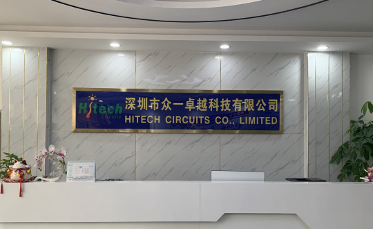
As a leading one-stop electronics manufacturing services provider in China, Hitech Circuits Co., Limited offers high quality, cost effective and quick turn PCB board products, Printed Circuit board, PCB assembly, electronics assembly manufacturing, Electronic parts components sourcing services for your new products development.
With mature supply chain, talented design team, advanced manufacturing techniques and quality control systems, Hitech Circuits Co., Limited is able to provide one-stop electronics manufacturing services and solution for our customers to help them stand out in the marketplace.
4 notes
·
View notes
Text


Printed circuit board manufacturing which is our major business, I think you already know, we are a PCB manufacturer. We have 3 branch factories dedicated to Quick Turn PCB Prototypes Manufacturing, Small and Medium-volume Printed Circuit Board, FPC Manufacturing services and PCB assembly services. Our market target is the High Multilayer PCB, High Density PCB, Flexible PCB, Rigid-flex PCB, Heavy copper PCB, Rogers PCB, Ceramic PCB and Special Materials Printed Circuit Boards.
Also, we can help customer sourcing components, wire PCB assembly and provide one-stop service.
Hitech Group is capable of providing full turn-key and partial turn-key PCB assembly services. For full turn-key, we take care of the entire process, including manufacture of Printed Circuit Boards, procurement of components, order tracking, continuous monitoring of quality and final board assembly. Whereas for partial turn-key, the customer can provide the PCBs and certain components, and the remaining parts will be handled by us.
4 notes
·
View notes
Text
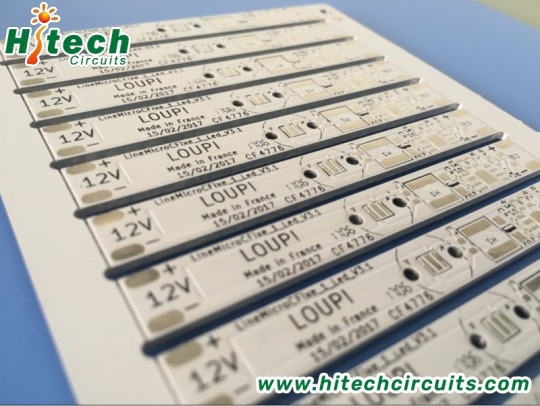

Aluminium PCB
Aluminium PCB are metal-based, copper-clad laminates with a good heat dissipation function. Usually, Aluminium PCB is refer to LED PCB board, which is the most important part of LED display and lighting products, etc.
Hitech Circuits Co., Limited is a professional aluminum pcb board, LED PCB manufacturer in China. Through 10 years of aluminum pcb board designing and manufacturing experience, Hitech are able to provide high quality and cost effective single layer, double layer and multi layer aluminum pcb boards to global customers. For any of your requirements regarding aluminum pcb board, please don’t hesitate to contact [email protected]
#Aluminium PCB#aluminum pcb#pcb assembly#pcb#engineering#technology#pcba#pcb manufacturer#pcbassembly#pcb design#hardware
5 notes
·
View notes
Text
One-stop PCB assembly service and PCB manufacturing supplier -- Hitechpcba
As a leading one-stop electronics manufacturing services provider in China, Hitech Circuits Co., Limited offers high quality, cost effective and quick turn PCB board products, Printed Circuit board, PCB assembly, electronics assembly manufacturing, Electronic parts components sourcing services for your new products development.
With mature supply chain, talented design team, advanced manufacturing techniques and quality control systems, Hitech Circuits Co., Limited is able to provide one-stop electronics manufacturing services and solution for our customers to help them stand out in the marketplace.
4 notes
·
View notes
Text
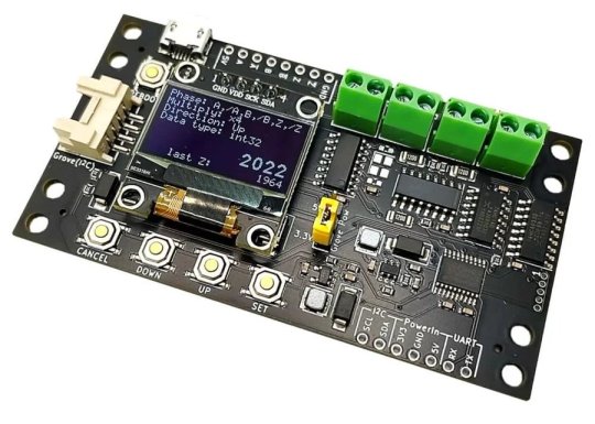
📢 Elecrow #PartnerSeller Program Product #Newarrival 🔥
🔱 Introducing the #EncoderCounter, meticulously designed by Y2Kb! This advanced device accurately displays and outputs the count of incremental output encoder pulses. 😻 #ElecrowPCB
🚀 #PCBA, selling, and shipping services provided by #Elecrow. For more info 👇
https://www.elecrow.com/encoder-counter.html?utm_source=tumblr&utm_term=idd=2
2 notes
·
View notes
Text
#hardware design#hardware design services#pcb assembly#pcb design#pcb manufacturer#pcba#pcbassembly#electronics design#automotive electronics
2 notes
·
View notes
Text
Printed Circuit Board Basics
Most of us are using Printed Circuit Board in our daily life. Printed Circuit Boards are used in almost all the Electronic products, from consumer gadgets such as PCs, tablets, smartphones, and gaming consoles to industrial and even high tech products in strategic and medical electronics domains.
Here, we have some statistics for you that shows how many electronic devices connect worldwide from 2015 to 2025. This statistic shows an increase in the use of a number of PCB in people daily life. Hence, CircuitWala took this opportunity to provide a basic knowledge about PCB via this article.
There are so many books available online which teach about Printed Circuit Board design and hardware part. There are few links available online which shows only a few basic fundamentals of PCB and few are there for Basics of Printed Circuit Board (PCB) Design. Few which gives good know knowledge on Printed Circuit Board terminology. But in the end for the hobbyist, there is no such material available which make their work easy.
Now days there few online designing websites available which allow hobbyist and students to create their design and Printed Circuit Board fabrication part. These websites provide limited features and charge high for the full edition. We, @CircuitWala are in try to provide one platform which provides plenty of Printed Circuit Board knowledge digitally to make your work simple and easy.
Alternatives of PCB include wire wrap and point-to-point construction. Creating a layout of PCB is a little bit time-consuming method as compared to its alternative solution but manufacturing of PCB is cheaper and faster then other wiring methods as electronic components are mounted and wired with one single part.
Let’s start with some basics of Printed Circuit Board with this article. Here in this article we will discuss about history of PCB to understand the emerge of PCB, Types of PCB to make your complex PCB a very simple using different types, Usage of PCB to provide you an idea to create more Printed Circuit Board projects, Advantages and Disadvantages, Possible Future to know about new technological change in Printed Circuit Board manufacturing and also about how to destroy and manage your PCB’s e-waste? We know you are eager to know all the stuff in details but before that let’s make a simple definition of Printed Circuit Board.
What is Printed Circuit Board?Printed Circuit Board is an electronic device made of conductive material(FR-4) like copper which connects components mounted on it to to get desired output by providing an input on another end.
When the board has not mounted with any of the components is called as Printed Circuit Board or Printed Wired Board. Mounting of an electronic component on Printed Circuit Board is called as PCB assembly.
History of Printed Circuit BoardThe invention of Printed Circuit Board was by Austrian engineer Paul Eisler as part of a radio set while working in England around 1936.
In early days before Printed Circuit Board became common in use, Point-to-Point construction was used. This meant some bulky and unreliable design that required plenty of sockets and regular replacement of it. Most of this issue directly address when PCB went into regular production.
Originally, every electronic component had wire leads, and the PCB had holes drilled for each wire of each component. The components’ leads were then passed through the holes and soldered to the PCB trace. This method of assembly is called Through-Hole construction. There is one other method to mount component is called as Surface Mount.
Type of Printed Circuit BoardPCBs are produced from the different types of material and on the basis of that material PCBs are divided mainly into two parts: Rigid PCB and Flexible PCB. Nowadays, a combination of Rigid and flexible PCB is also possible and that is called as Flexi-Rigid PCBs.
Most of the PCBs are built in layers. The inner layer is the base material called as a substrate. Rigid PCBs are mainly made of material like epoxy materials and Flexible PCBs are made of plastic material that can withstand high temperatures.
Rigid PCBs are generally, hard materials that hold the component in a better way. The motherboard in the tower of a computer is the best example of Rigid PCBs. Flexible PCBs fundamental material allows PCB to fit into forms that Rigid PCBs can not. Flexible PCBs can turn round without harmful the circuit on PCB.
All Rigid and Flexible PCBs can come in three formats by layers: Single Layer, Double Layer, and Multi-Layer.
1. Single Layer PCBSingle Layer PCBs have been around since the late 1950s and still dominate the world market in sheer piece volume. Single Sided PCBs contain only one layer of conductive material and are best suited for low-density designs. Single-sided PCBs are easy to design and quick to manufacture. They serve as the most lucrative platform in the industry.
2. Double Layer PCBDouble Layered printed circuit board technology is conceivably the most popular type of PCB in the industry. Double Sided PCB (also known as Double-Sided Plated Thru or DSPT) circuits are the gateway to advanced technology applications. They allow for a closer (and perhaps more) routing traces by alternating between top and bottom layers using vias.
3. Multi Layer PCB
Multilayer PCB is a circuit board that has more than two layers. Unlike a Double-Sided PCB which only has two conductive layers of material, all multilayer PCBs must have at least three layers of conductive material which are buried in the center of the material.
Usage of Printed Circuit BoardBy reading this article till this point, we hope that you are now able to get about printed circuit boards. Now, we will make you understand about different applications of printed Circuit Board.
In this digital world, Printed Circuit Board is in almost all our daily life electronic devices and in our industrial electronics as well. Below are the industries where PCBs are used:
Possible FutureNowadays, most of the circuits are replaced to produce Printed Circuit Board from the old methods. Revolution in technology made many of the processes automated and hence it is easy to manufacture PCB. But still, these processes are a bit expensive to hire, involve toxic waste and use high temperatures and acids. With technological advances we have seen in the past years, it is not hard to imagine PCB will soon be revolutionized. Not only that but research institutes predict a more ‘green’ future for PCBs; PCBs being made of paper.
Electronic Waste (e-waste)Electronic Waste or e-waste is described as discarded electrical or electronic devices. Informal processing of e-waste in developing countries can lead to adverse human health effects and environmental pollution.
Electronic scrap components contain a hazardous substance such as lead, cadmium, beryllium, or brominated flame retardants. Recycling and disposal of e-waste may involve significant risk to health of workers and communities in developed countries and great care must be taken to avoid unsafe exposure in recycling operations
Nowadays, developing countries are encouraging electronic users to take care while recycling the e-waste or submit them to the organization who are involved in such activities.
SummaryIn this blog, we have learned the basics of Printed Circuit Board. CircuitWala is planning to write as many blogs to provide more and more knowledge of Printed Circuit Board. Either it is basics or manufacturing or usages or advantages and disadvantages of PCBs. We will also try to make our users/customers up to date for the new technology innovations, including past histories and revolution of the PCB industries.
In the next blog, we will look at more briefly about the different types of Printed Circuit Board. We also understand the process to make it and different usage and application for the same.
#electronic circuit design company#pcb circuit manufacturer in ahmedabad#pcb design & manufacturing services#printed circuit board companies#printed circuit board order online#PCB manufacturer#Printed Circuited Board#double layer PCB#PCB Quality Control
2 notes
·
View notes
Text

#pcb#pcba#pcbassembly#aluminum pcb#pcb design#pcb fabrication#pcb factory#pcb manufacturer#pcb board#pcb prototype
2 notes
·
View notes
Text

We are a 20 years PCB&PCBA factory.
4 notes
·
View notes
Text
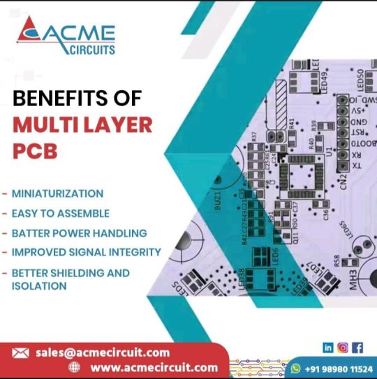
Multilayer PCBs (Printed Circuit Boards) offer numerous advantages over their single-layer or double-layer counterparts. These benefits arise from their enhanced design capabilities, improved performance, and greater flexibility. Here are some key advantages of multilayer PCBs:
#PCB#printed circuit board manufacturers#electronic cable assembly#pcb manufacturing#pcb assembly manufacturer#pcb assembly services#pcb board manufacturer#printed circuit board manufacturer in india#circuit board manufacturing#pcb exporters#pcba#pcb manufacturer#pcb design#pcbassembly#multilayer pcb
2 notes
·
View notes
Last Seen Blogs