#Waveguide Filter
Explore tagged Tumblr posts
Visit Tumblr Blog
Explore Tumblr blogs with no restrictions, modern design and the best experience.
Last Seen Tumblr Blogs


Fun Fact
There are dozens of funny blogs to kill time on Tumblr.
Text
Environmental Monitoring Devices Go Ultra-Sensitive with Nano Light
The global nanophotonics market, valued at USD 25.6 billion in 2023 and projected to surpass USD 45 billion by 2031 at a CAGR of 7.9%, is witnessing robust growth driven by rising innovation in telecommunications and increasing R&D investments, particularly in North America. Nanophotonics enables manipulation of light at the nanoscale, revolutionizing applications in optoelectronics, displays, and biomedical imaging. Market competition is intensifying with key players like EPISTAR Corporation, Samsung SDI Co Ltd., and OSRAM Licht AG expanding their technological capabilities to capture emerging opportunities across industries.

Unlock exclusive insights with our detailed sample report :
Key Market Drivers
1. Growing Demand for Faster, Low-Energy Data Transmission
With explosive data generation, data centers and cloud systems demand ultra-fast, energy-efficient data transfer. Nanophotonic components like photonic integrated circuits (PICs) are revolutionizing how data is moved, processed, and stored.
2. Surge in LED and OLED Technologies
Widespread adoption of LED and OLED displays in televisions, smartphones, automotive dashboards, and wearable tech has significantly increased the demand for nanophotonic light emitters and filters, especially those based on quantum dots and plasmonics.
3. Advancements in Photonic Chips for AI and Machine Learning
AI and high-performance computing are integrating nanophotonic optical interconnects into chips to minimize latency and heat, improving processing speeds while reducing energy consumption.
4. Quantum Computing and Security Applications
Nanophotonics is fundamental to quantum communication and cryptography, enabling high-speed, unbreakable data transmission protocols through single-photon sources and waveguides.
5. Rising Applications in Biophotonics and Healthcare
Non-invasive medical diagnostics, biosensors, and real-time imaging are leveraging nanophotonic sensors to achieve superior sensitivity, resolution, and accuracy, especially in cancer detection and genomic sequencing.
Regional Trends
United States
The U.S. nanophotonics market benefits from:
Robust semiconductor policy investments such as the CHIPS Act.
Heavy investments by firms like Intel, NVIDIA, and IBM in optical computing, including photonics-powered AI accelerators.
Collaborations with universities like MIT and Stanford, advancing research in light-based transistors, plasmonic circuits, and meta-optics.
Expansion into military-grade nanophotonics, especially for secure communication and space-grade sensors.
Japan
Japan remains a global leader in:
Miniaturized optics for automotive lidar, biomedical tools, and AR/VR headsets.
Integration of nanophotonics into robotics and factory automation, essential to Industry 5.0.
Development of compact biosensors using metallic nanostructures and quantum dots for use in home diagnostics and elderly care.
Notable progress is being made by companies such as Hamamatsu Photonics, Panasonic, and Sony, in collaboration with R&D institutes like RIKEN and NIMS.
Speak to Our Senior Analyst and Get Customization in the report as per your requirements:
Industry Segmentation
By Product:
Light-Emitting Diodes (LEDs)
Organic LEDs (OLEDs)
Photonic Integrated Circuits (PICs)
Optical Switches
Solar Photovoltaic Devices
Laser Diodes
Near-field Optical Components
By Material:
Plasmonic Nanostructures
Photonic Crystals
Semiconductor Quantum Dots
Carbon Nanotubes
Nanowires
By Application:
Consumer Electronics
Telecommunications
Healthcare & Life Sciences
Defense & Aerospace
Energy and Solar Cells
Automotive & Smart Mobility
Latest Industry Trends
AI Chips Powered by Nanophotonics U.S. startups are integrating light-based transistors into neural processors, enabling ultrafast computation with reduced energy overhead.
Next-Gen Displays with Quantum Dot Emitters Quantum dots embedded in nanophotonic architectures improve brightness, color fidelity, and efficiency in displays across smartphones and TVs.
Photonic Neural Networks in Development Light-based neural nets are being tested in Japan and the U.S. to replace electrical interconnects in deep learning hardware.
Nanophotonic Biosensors for Real-Time Diagnostics Portable nanophotonic devices for glucose monitoring, cancer markers, and airborne pathogen detection are gaining traction post-pandemic.
Flexible and Wearable Nanophotonic Devices Researchers are developing bendable and transparent photonic circuits for integration into smart textiles and wearable health trackers.
Buy the exclusive full report here:
Growth Opportunities
Data Center Optics: Expanding demand for optical interconnects in hyperscale data centers.
Automotive LiDAR and Optical Sensors: Nanophotonic lidar solutions are being miniaturized for next-gen autonomous driving.
Healthcare and Point-of-Care Devices: Growing use of on-chip diagnostic tools in both clinical and at-home settings.
5G & Beyond: Nanophotonics supports the backbone of high-speed network infrastructure with integrated optical circuits.
Space and Defense: Lightweight, ultra-sensitive nanophotonic sensors for space exploration, drones, and military surveillance.
Competitive Landscape
Major players in the global nanophotonics market include:
Intel Corporation
NKT Photonics
Hamamatsu Photonics
Samsung Electronics
Mellanox Technologies (NVIDIA)
Sony Corporation
Osram Licht AG
Luxtera (Cisco)
IBM Corporation
Mellanox Technologies
These companies are investing in:
Photonics foundries and wafer-level integration.
Startups and university spin-offs focused on next-gen light control and biosensing.
Joint ventures for scaling quantum and optical chip production.
Stay informed with the latest industry insights-start your subscription now:
Conclusion
The nanophotonics market is emerging as a pivotal enabler across a wide spectrum of industries—from semiconductors and smart electronics to biotech and energy systems. As global demand intensifies for faster data transmission, energy efficiency, and miniaturization, nanophotonics offers scalable, sustainable solutions.
With leading countries like the United States and Japan investing heavily in R&D, infrastructure, and commercialization strategies, the market is entering a phase of high-value growth and disruption. The convergence of nanotechnology, AI, and photonics is shaping a future defined by faster, smarter, and more resilient technologies.
About us:
DataM Intelligence is a premier provider of market research and consulting services, offering a full spectrum of business intelligence solutions—from foundational research to strategic consulting. We utilize proprietary trends, insights, and developments to equip our clients with fast, informed, and effective decision-making tools.
Our research repository comprises more than 6,300 detailed reports covering over 40 industries, serving the evolving research demands of 200+ companies in 50+ countries. Whether through syndicated studies or customized research, our robust methodologies ensure precise, actionable intelligence tailored to your business landscape.
Contact US:
Company Name: DataM Intelligence
Contact Person: Sai Kiran
Email: [email protected]
Phone: +1 877 441 4866
Website: https://www.datamintelligence.com
#Nanophotonics market#Nanophotonics market size#Nanophotonics market growth#Nanophotonics market share#Nanophotonics market analysis
0 notes
Text
Algorithm Trading Market Growth Analysis 2025
The global Algorithm Trading market was valued at US$ 13,523.37 million in 2023 and is anticipated to reach US$ 26,730.34 million by 2030, witnessing a CAGR of 10.58% during the forecast period 2024-2030.
Get free sample of this report at : https://www.intelmarketresearch.com/download-free-sample/270/algorithm-trading
North American market for Algorithm Trading is estimated to increase from $ 6,319.47 million in 2023 to reach $ 12,357.44 million by 2030, at a CAGR of 10.46% during the forecast period of 2024 through 2030.
Asia-Pacific market for Algorithm Trading is estimated to increase from $ 3,179.34 million in 2023 to reach $ 6,353.80 million by 2030, at a CAGR of 10.73% during the forecast period of 2024 through 2030.
The global market for Algorithm Trading in Investment Bank is estimated to increase from $ 6,852.29 million in 2023 to $ 13,381.21 million by 2030, at a CAGR of 10.39% during the forecast period of 2024 through 2030.
The major global companies of Algorithm Trading include QuantConnect, 63 moons, InfoReach, Argo SE, MetaQuotes Software, Automated Trading SoftTech, Tethys Technology, Trading Technologies, and Tata Consultancy Services, etc. In 2023, the world's top three vendors accounted for approximately 22.52 % of the revenue.
This report aims to provide a comprehensive presentation of the global market for Algorithm Trading, with both quantitative and qualitative analysis, to help readers develop business/growth strategies, assess the market competitive situation, analyze their position in the current marketplace, and make informed business decisions regarding Algorithm Trading.
The Algorithm Trading market size, estimations, and forecasts are provided in terms of and revenue ($ millions), considering 2023 as the base year, with history and forecast data for the period from 2019 to 2030. This report segments the global Algorithm Trading market comprehensively. Regional market sizes, concerning products by Type, by Application, and by players, are also provided.
For a more in-depth understanding of the market, the report provides profiles of the competitive landscape, key competitors, and their respective market ranks. The report also discusses technological trends and new product developments.
The report will help the Algorithm Trading companies, new entrants, and industry chain related companies in this market with information on the revenues for the overall market and the sub-segments across the different segments, by company, by Type, by Application, and by regions.
Market Segmentation
By Company
QuantConnect
63 moons
InfoReach
Argo SE
MetaQuotes Software
Automated Trading SoftTech
Tethys Technology
Trading Technologies
Tata Consultancy Services
Exegy
Virtu Financial
Symphony Fintech
Kuberre Systems
Itexus
QuantCore Capital Management
Segment by Type
Forex Algorithm Trading
Stock Algorithm Trading
Fund Algorithm Trading
Bond Algorithm Trading
Cryptographic Algorithm Trading
Other Algorithmic Trading
Segment by Application
Investment Bank
Fund Company
By Region
North America
United States
Canada
Others
Asia-Pacific
China
Japan
South Korea
Southeast Asia
India
Rest of Asia
Europe
Germany
France
U.K.
Rest of Europe
South America
Mexico
Brazil
Argentina
Rest of South America
Middle East & Africa
Middle East
Africa
Get free sample of this report at : https://www.intelmarketresearch.com/download-free-sample/270/algorithm-trading
0 notes
Text
0 notes
Text
0 notes
Text
Have your PIC-based devices been tested reliably and quickly?
Photonic Integrated Circuit (PIC) solutions are being adopted by manufacturers to address the reduced size and complexity challenges while also addressing heat management issues experienced in today’s data centres. Frantic development of smaller, faster, cheaper and greener transceivers/active components and passive components is driving the development of high-speed networks and 5G, Photonic Integrated Circuits (PICs).
Passive optical components used in optical systems operate without external power or active control. They use processes such as transmission, reflection, polarisation, coupling, splitting, filtering, and attenuation to alter light signals.
Need for Testing
A PIC is composed of many optical components such as optical couplers, fibre-optic switches, splitters, attenuators, wavelength-division multiplexers, and transceivers.
Testing of any PIC-based device is needed in all life cycle stages — from design and development, and qualification to validation of production.
Testing – The Requirements
Automation, repeatability, scalability and parallelisation of the testing processes are needed for the huge volume of circuits and ports, to be able to meet the profitability of economies of scale. Photonics labs must evolve with the optical test requirements of passive (guiding light) optical components.
The fast maturing PIC die manufacturing has given rise to photonic wafers containing thousands of components made available by foundries through Process Design Kits (PDKs). Reliable testing is needed to optimise the different parameters of a given optical component.
Testing – The Challenges
Accuracy/repeatability: Obtaining traceable results for tight acceptance thresholds and greater yield of known good dies.
Dynamic range: Seeing full optical spectral contrast in a single measurement.
Speed: Keeping alignment and measurement time to a minimum, but also accelerating the ease of the test and analysis iterative flow.
From data to insight: Generating and managing structured data that is ready for artificial intelligence and business intelligence.
Flexible/scalable: Leveraging test station modularity and third-party compatibility of software to improve test throughput and complexity over time or swap equipment as needed.
Automation: Automating chip and wafer advanced navigation to control any instrument and execute data analysis in user-defined test routines to test massive circuits with minimal cost of ownership.
Testing PIC-based passive components is challenging due to the high port count of some components like Arrayed Waveguide Grating (AWG) and the huge number of components to test on a single die. A component test platform operates in conjunction with a continuously tunable laser to measure optical insertion loss, return loss and polarisation-dependent loss across the laser’s spectral range. Optical spectrum must be realised quickly and with a high wavelength resolution, typically to the order of a picometer.
Testing – The Process
The PIC devices are usually tested at the wafer level prior to dicing to detect defects as early as possible and to avoid packaging defective dies.
Using a PIC wafer probe station, light is coupled into the wafer to enable measurement of the optical characteristics of the DUT.
Testing Solutions for Photonics from MELSS
MELSS brings you Test and Measurement (T&M) hardware and software solutions from market leaders EXFO, which are automated, scalable, fast, accurate and cost-optimised. These T&M solutions range from those for Passive and Active components as well as automated probe stations for wafer and single-die testing.
The OPAL series of probe stations deliver industry-leading performance for testing wafers, multiple as well as single dies, enabling accurate, repeatable and fast measurement. The PILOT software suite offers automation capabilities that support the full test flow (preparation through measurement to results analysis), using EXFO’s or third-party T&M instruments.
EXFO’s comprehensive range of optical testing solutions includes component test platforms, optical testing solutions, light sources, benchtop tunable lasers, passive component testers, optical spectrum analysers, tunable filters with adjustable bandwidth, variable attenuators, switches and power meters.
EXFO has developed automated, scalable, fast, accurate and cost-effective Test and Measurement (T&M) hardware and software solutions. Ranging from simple optical testing to spectral optical characterisation or traffic analysis, EXFO offers an extensive selection of probe stations for wafer, bar, multi-die or single die configurations, and a powerful automation software suite.
The CTP10 from EXFO specifically addresses key PIC measurement challenges. measuring optical components quickly, reliably and accurately.
The CTP10 is a modular component test platform that operates together with the T200S or T500S continuously tunable lasers. The CTP10 characterises the spectral properties of high port count devices in one single scan with
High spectral resolution
70-dB dynamic range, even at a sweep speed of 200 nm/s
Operation from 1240 to 1680 nm
Coverage of a wide range of applications, including telecom, sensing and LIDAR.
Both optical and photocurrent measurements with analog output for PIC first-light search and coupling optimisation
Fast data transfer
Remote control using SCPI commands is possible
Increased PIC testing throughput
Reduced test time
High sampling resolution of 20 fm
Accurate measurement of narrow spectral features
The CT440 is a compact variant of the CTP10, with the same performance – ideal for the characterisation of PIC components with limited outputs.
In addition to the above range of products, EXFO produces other advanced products such as the T200S, T500S, CTP10, CT440, OSICS T100, FTBx-2850 and OSA20.
Author: MELSS
0 notes
Text
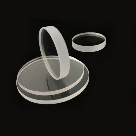
The Revolutionary Application of Quartz Plate in Semiconductor Packaging
The Revolutionary Application of Quartz Plate in Semiconductor Packaging: Why These Four Designs Are Game-Changers Let’s cut through the noise: semiconductor packaging isn’t just about chips anymore—it’s about the materials that cradle them. Quartz plates, once relegated to lab equipment, are now the unsung heroes of microelectronics. But not all quartz is created equal.
I’ve seen firsthand how four specific designs—round transparent quartz glass plates, tempered quartz sight glass, OEM customized optical square/round quartz glass plates, and square UV transparent quartz plates—are rewriting the rules of reliability and precision. Here’s why they matter.
1. Round Transparent Quartz Glass Plates: The Purity Powerhouse
Imagine a material so pristine it makes surgical steel look rusty. Round transparent quartz plates, with >99.99% SiO₂ purity, are the gold standard for wafer handling in extreme environments. Take TSMC’s 3nm node fab: by replacing ceramic carriers with these plates, they reduced particulate contamination by 78% during high-temperature annealing1. The secret? Zero metallic ions means no unwanted doping—critical when a single stray atom can wreck a billion-transistor chip.
But purity isn’t their only trick. Their thermal stability (up to 1,200°C) allows rapid thermal processing (RTP) cycles without warping—a feat that aluminum nitride plates fail at after 50 cycles.
2. Tempered Quartz Sight Glass: When Failure Isn’t an Option
Vacuum chambers in EUV lithography systems demand visibility and invincibility. Tempered quartz sight glass, chemically strengthened via ion exchange, laughs at 10⁻⁸ Torr pressures while providing distortion-free inspection windows. ASML’s latest EUV machines use these panels to monitor plasma arcs—where standard fused silica would cloud within weeks under 13.5nm radiation.
The kicker? Their surface hardness (9 Mohs) prevents scratches from robotic handlers—eliminating the “fogged window” failures that once caused 12% of lithography tool downtime.
3. OEM Customized Optical Square/Round Quartz Plates: Geometry Meets Photonics
Why settle for off-the-shelf when light manipulation demands perfection? Customized optical quartz plates, with sub-λ/4 flatness, are enabling breakthroughs in chip-scale photonics. Intel’s optical interconnects team credits square quartz plates—etched with nanoscale grating patterns—for achieving 92% light coupling efficiency in their silicon photonics modules12. The rectangular edges align perfectly with waveguide arrays, something round plates can’t match.
But round variants shine too: their radial symmetry minimizes stress birefringence in laser diode packaging—a must for 800G DR4 transceivers.
4. Square UV Transparent Quartz Plates: The Dark Horse of Advanced Packaging
UV-curing adhesives are the glue holding 2.5D/3D packages together—literally. Square UV quartz plates, transmitting >90% at 254nm, ensure uniform curing while blocking IR heat that warps interposers. Samsung’s HBM4 stack line reported a 30% yield boost after switching to these plates, as their sharp corners align with die edges to prevent adhesive bleed-out.
Bonus: Their UV transparency doubles as a built-in quality check—uncured resin fluoresces under 365nm light, visible through the plate.

Why This Isn’t Just Progress—It’s a Paradigm Shift
Critics argue quartz is “too brittle” or “too niche.” Tell that to the engineers who’ve seen:
Round plates slash cleanroom particle counts by filtering airborne contaminants during robotic transfers.
Square UV plates enable fan-out wafer-level packaging (FOWLP) for wearables, where 0.1mm thickness tolerances are non-negotiable.
While graphene and GaN hog headlines, quartz plates work silently in the trenches—enabling the angstrom-scale precision our connected world demands.
The Bottom Line In semiconductor packaging, the difference between “functional” and “flawless” lies in the materials you trust. These four quartz plate designs aren’t just components—they’re enablers of a future where chips aren’t just smaller, but smarter. If your supply chain hasn’t embraced them yet, you’re not just behind the curve—you’re ignoring the bedrock of modern electronics.
0 notes
Text
0 notes
Text
High Frequency Board Design
High-frequency PCB design is a specialized field that requires careful attention to signal integrity, impedance control, and electromagnetic interference (EMI) mitigation. Designing a PCB for high-frequency signals (typically above 100 MHz) or microwave frequencies (GHz range) demands a solid understanding of electrical engineering principles and the unique properties of materials and components at high frequencies.
Key Considerations in High-Frequency PCB Design:
1. Signal Integrity and Transmission Lines
Transmission Line Effects: At high frequencies, the PCB trace behaves like a transmission line, and signal degradation can occur if not properly designed. Transmission line impedance must be matched to the source and load impedance to avoid reflections.
Impedance Control: The characteristic impedance (typically 50 ohms for RF signals) of traces should be precisely controlled. The design needs to ensure that trace width, spacing, and the dielectric material thickness are optimized for the desired impedance.Microstrip Lines: These are traces on the surface of the PCB, with a reference plane (ground) below them.Stripline: Traces are sandwiched between two ground planes, providing better shielding and lower susceptibility to external EMI.Coplanar Waveguides: Similar to microstrips, but with the ground plane adjacent to the signal trace.
2. Material Selection
High-frequency PCBs require materials with low loss and stable dielectric properties at high frequencies:
PTFE-based materials like Rogers laminates, Teflon, and ceramic materials are common choices because they offer low loss and stable electrical performance.
FR-4 can be used for lower-frequency applications, but higher-performance materials are preferred for GHz designs due to the higher loss tangent of FR-4 at high frequencies.
3. Component Placement
Minimize Trace Lengths: The shorter the trace, the lower the loss and the higher the signal integrity. High-frequency signals degrade over distance due to resistance, capacitance, and inductance.
Strategic Grounding: Grounding is crucial for high-frequency PCBs. Poor grounding can cause noise, EMI, and ground bounce. Ensure the PCB has a solid, continuous ground plane and use via stitching to connect the ground planes together.
Decoupling Capacitors: These are used to filter out noise from power supply lines. At high frequencies, the placement of decoupling capacitors should be as close as possible to the components to reduce inductance.
4. Cross-Talk and EMI Control
Reduce Cross-Talk: Cross-talk between adjacent signal traces can cause unwanted coupling of signals. To minimize this, maintain a sufficient distance between traces carrying high-speed signals or use ground planes to shield them.
EMI Shielding: High-frequency designs are more susceptible to EMI. Techniques like using shielding cans, keeping high-frequency traces short, and maintaining a continuous ground plane can help mitigate EMI. Additionally, proper via placement and PCB layer stacking are critical in controlling the return currents of high-frequency signals.
5. Via Design
Via Inductance: Vias introduce inductance, which can degrade signal integrity at high frequencies. Microvias (small vias) and buried vias are used to reduce the inductance of traditional vias.
Via Size: Keep via sizes small to reduce their impact on the signal path. A smaller via reduces its inductance, making it less of a bottleneck at high frequencies.
6. Thermal Management
High-frequency signals generate heat, so thermal management is crucial in high-frequency PCB designs. Ensure that heat can dissipate from components and traces by using thermal vias, heat sinks, and adequate spacing between high-power components.
In some cases, ceramic PCBs are used because of their excellent thermal conductivity.
7. Simulation and Testing
Simulations: Use simulation tools like HFSS, ADS (Advanced Design System), and Ansys to simulate the behavior of high-frequency circuits before fabrication. This helps to verify signal integrity, impedance matching, and EM radiation.
Prototyping and Testing: After fabrication, high-frequency PCBs should be tested using tools like vector network analyzers (VNA) and time-domain reflectometers (TDR) to measure the reflection and loss of signals at various frequencies.
Design Process for High-Frequency PCBs:
Step 1: Understand the Frequency Range and Requirements
Identify the frequency range the design will operate in and the critical parameters like impedance, signal-to-noise ratio, and power handling capabilities.
Step 2: Choose the Right Materials
Based on the frequency and performance requirements, select appropriate PCB materials (e.g., PTFE, ceramic, Rogers laminates) that offer low loss and stable dielectric properties.
Step 3: Design Transmission Lines
Use tools like CAD software (e.g., Altium Designer, Eagle, OrCAD) to design traces that maintain controlled impedance and avoid sharp turns in the signal paths.
Implement proper via types and trace geometries for impedance matching.
Step 4: Grounding and Shielding
Ensure continuous and solid grounding to minimize noise and EMI.
Use ground planes for shielding and reduce cross-talk between high-frequency traces.
Step 5: Component Selection and Placement
Choose components that are designed for high-frequency applications (e.g., low parasitic inductance and capacitance).
Place components close to one another and ensure the power and ground planes are properly integrated.
Step 6: Use Simulation Tools
Before finalizing the design, simulate the circuit’s behavior using electromagnetic simulation software. This helps identify potential problems with signal integrity, impedance mismatch, and power delivery.
Step 7: Prototyping and Testing
Fabricate a prototype and perform tests like S-parameter measurements, time-domain reflectometry (TDR), and network analysis to ensure the PCB operates as expected in the high-frequency range.
Common Applications of High-Frequency PCBs:
Telecommunications: For RF circuits, antennas, and communication devices.
Microwave and Radar Systems: For military, aerospace, and scientific applications.
Satellite Communication: For high-frequency signal transmission in space systems.
Consumer Electronics: In products like smartphones, Wi-Fi devices, and Bluetooth.
Automotive: For radar systems and wireless communication in vehicles.
Conclusion:
High-frequency PCB design requires specialized knowledge of electromagnetic theory, materials science, and circuit design. By focusing on key areas like signal integrity, impedance control, and EMI management, engineers can ensure that high-frequency circuits perform reliably even at the most challenging frequencies. Proper simulation and testing are essential to validate the design and avoid performance issues during real-world use.
Let me know if you need more details or specific resources on any of these topics!

0 notes
Text
0 notes
Text
Aerogel Insulation Market Growth Analysis 2025
The global Aerogel Insulation market was valued at US$ 757.24 million in 2023 and is anticipated to reach US$ 1,946.62 million by 2030, witnessing a CAGR of 14.37% during the forecast period 2024-2030.
Get free sample of this report at :https://www.intelmarketresearch.com/download-free-sample/330/aerogel-insulation Aerogel insulation is a type of insulation material made of aerogel, which is a solid with a very low density and very low thermal conductivity. It's sometimes referred to as "frozen smoke" or "solid smoke" because of its lightness and transparency. Aerogel is produced by removing the liquid component from a gel, resulting in a solid material that can be up to 95% air by volume. This makes it an excellent insulator, as air is a very poor conductor of heat. This report aims to provide a comprehensive presentation of the global market for Aerogel Insulation, with both quantitative and qualitative analysis, to help readers develop business/growth strategies, assess the market competitive situation, analyze their position in the current marketplace, and make informed business decisions regarding Aerogel Insulation. The Aerogel Insulation market size, estimations, and forecasts are provided in terms of and revenue ($ millions), considering 2023 as the base year, with history and forecast data for the period from 2019 to 2030. This report segments the global Aerogel Insulation market comprehensively. Regional market sizes, concerning products by Type, by Application, and by players, are also provided.For a more in-depth understanding of the market, the report provides profiles of the competitive landscape, key competitors, and their respective market ranks. The report also discusses technological trends and new product developments. The report will help the Aerogel Insulation companies, new entrants, and industry chain related companies in this market with information on the revenues for the overall market and the sub-segments across the different segments, by company, by Type, by Application, and by regions. Market SegmentationBy Company
Aspen Aerogels
Cabot Corporation
IBIH
Nano Tech
Guangdong Alison Technology
Van-Research Innovation
Shenzhen Aerogel Technology
Armacell
Enersens
Aerogel Technologies
Active Aerogels
Xiamen Namate New Materials
Beerenberg
Segment by Type
Blankets
Granules and Powders
Other
Segment by Application
Oil and Gas
Building Insulation
Transportation
Household Appliances
Aerospace and Military
Other
By RegionNorth America
United States
Canada
Asia-Pacific
China
Japan
Korea
India
Southeast Asia
Australia
Rest of Asia-Pacific
Europe
Germany
France
U.K.
Italy
Russia
Rest of Europe
Latin America
Mexico
Brazil
Rest of Latin America
Middle East & Africa
Middle East
Get free sample of this report at :https://www.intelmarketresearch.com/download-free-sample/330/aerogel-insulation
https://intel24.hashnode.dev/frac-valves-market-growth-analysis-2025
https://intel24.hashnode.dev/fertigation-system-market-growth-analysis-2025
https://intel24.hashnode.dev/carbomer-market-growth-analysis-2025-2032
https://intel24.hashnode.dev/ceramic-dielectric-waveguide-filter-market-growth-analysis-2025
https://intel24.hashnode.dev/chromatic-confocal-sensors-market-growth-analysis-2025
https://intel24.hashnode.dev/cabin-for-construction-machinery-market-growth-analysis-2025
https://intel24.hashnode.dev/anti-reflective-window-film-market-growth-analysis-2025
https://intel24.hashnode.dev/5g-antennas-market-growth-analysis-2025
https://intel24.hashnode.dev/hplc-columns-market-growth-analysis-2025
https://intel24.hashnode.dev/acetophenone-market-growth-analysis-2025
0 notes
Text
0 notes
Text
SYNTHWAVECPU N12:Photonics Session 4

Microring resonators (MRRs) have emerged as a promising technology for neuromorphic computing, due to their ability to perform complex signal processing operations using optical signals. MRRs are small, circular waveguides that can be fabricated on a chip using standard semiconductor manufacturing processes. They can be used to generate and manipulate optical signals with high precision and low power consumption, making them suitable for applications in high-performance computing and communication systems.One of the key advantages of MRRs for neuromorphic computing is their ability to perform nonlinear signal processing operations. When a high-intensity optical signal is injected into an MRR, it can induce nonlinear effects that can be used for various functionalities, including spike generation and tunable filtering. By integrating MRRs with other optical components, it is possible to form optical spiking neurons that can receive optical inputs, generate optical spikes, and transmit them to other neurons via optical channels.The tunable filtering capabilities of MRRs can also be used to implement synaptic plasticity, where the strength of connections between spiking neurons can be modulated, mimicking the learning and memory processes of biological synapses. This is an important feature for neuromorphic computing, as it enables the development of adaptive neural networks that can learn and evolve over time.In recent years, add-drop microring resonators (ADMRRs) have gained attention for their potential in neuromorphic computing. ADMRRs are a type of MRR that can be configured in an add-drop configuration, which allows for precise control over the resonant modes and light propagation within the ring. This enables the implementation of complex signal processing operations, such as weighting and filtering, with high precision and low power consumption. In terms of future work, there are several research directions that can be pursued to further advance the use of ADMRRs for neuromorphic computing. One direction is to investigate the use of different materials for the fabrication of ADMRRs, such as silicon nitride and silicon oxynitride, which can offer improved performance and stability. Another direction is to explore the use of different geometries and configurations for ADMRRs, such as coupled-resonator optical waveguides (CROWs) and photonic crystal resonators, which can offer improved performance and scalability.
0 notes
Text
Have your PIC-based devices been tested reliably and quickly?
Photonic Integrated Circuit (PIC) solutions are being adopted by manufacturers to address the reduced size and complexity challenges while also addressing heat management issues experienced in today’s data centres. Frantic development of smaller, faster, cheaper and greener transceivers/active components and passive components is driving the development of high-speed networks and 5G, Photonic Integrated Circuits (PICs).
Passive optical components used in optical systems operate without external power or active control. They use processes such as transmission, reflection, polarisation, coupling, splitting, filtering, and attenuation to alter light signals.
Need for Testing
A PIC is composed of many optical components such as optical couplers, fibre-optic switches, splitters, attenuators, wavelength-division multiplexers, and transceivers.
Testing of any PIC-based device is needed in all life cycle stages — from design and development, and qualification to validation of production.
Testing — The Requirements
Automation, repeatability, scalability and parallelisation of the testing processes are needed for the huge volume of circuits and ports, to be able to meet the profitability of economies of scale. Photonics labs must evolve with the optical test requirements of passive (guiding light) optical components.
The fast-maturing PIC die manufacturing has given rise to photonic wafers containing thousands of components made available by foundries through Process Design Kits (PDKs). Reliable testing is needed to optimise the different parameters of a given optical component.
Testing — The Challenges
Accuracy/repeatability: Obtaining traceable results for tight acceptance thresholds and greater yield of known good dies.
Dynamic range: Seeing full optical spectral contrast in a single measurement.
Speed: Keeping alignment and measurement time to a minimum, but also accelerating the ease of the test and analysis iterative flow.
From data to insight: Generating and managing structured data that is ready for artificial intelligence and business intelligence.
Flexible/Scalable: Leveraging test station modularity and third-party compatibility of software to improve test throughput and complexity over time or swap equipment as needed.
Automation: Automating chip and wafer advanced navigation to control any instrument and execute data analysis in user-defined test routines to test massive circuits with minimal cost of ownership.
Testing PIC-based passive components is challenging due to the high port count of some components like Arrayed Waveguide Grating (AWG) and the huge number of components to test on a single die. A component test platform operates in conjunction with a continuously tunable laser to measure optical insertion loss, return loss and polarisation-dependent loss across the laser’s spectral range. The optical spectrum must be realised quickly and with a high wavelength resolution, typically to the order of a picometer.
Testing — The Process
The PIC devices are usually tested at the wafer level prior to dicing to detect defects as early as possible and to avoid packaging defective dies.
Using a PIC wafer probe station, light is coupled into the wafer to enable measurement of the optical characteristics of the DUT.
Testing Solutions for Photonics from MELSS
MELSS brings you Test and Measurement (T&M) hardware and software solutions from market leaders EXFO, which are automated, scalable, fast, accurate and cost-optimised. These T&M solutions range from those for Passive and Active components as well as automated probe stations for wafer and single-die testing.
The OPAL series of probe stations deliver industry-leading performance for testing wafers, multiple as well as single dies, enabling accurate, repeatable and fast measurement. The PILOT software suite offers automation capabilities that support the full test flow (preparation through measurement to results analysis), using EXFOs or third-party T&M instruments.
EXFOs comprehensive range of optical testing solutions includes component test platforms, optical testing solutions, light sources, benchtop tunable lasers, passive component testers, optical spectrum analysers, tunable filters with adjustable bandwidth, variable attenuators, switches and power meters.
EXFO has developed automated, scalable, fast, accurate and cost-effective Test and Measurement (T&M) hardware and software solutions. Ranging from simple optical testing to spectral optical characterisation or traffic analysis, EXFO offers an extensive selection of probe stations for wafer, bar, multi-die or single-die configurations, and a powerful automation software suite.
The CTP10 from EXFO specifically addresses key PIC measurement challenges. measuring optical components quickly, reliably and accurately.
The CTP10 is a modular component test platform that operates together with the T200S or T500S continuously tunable lasers. The CTP10 characterises the spectral properties of high port count devices in one single scan with
High spectral resolution
70-dB dynamic range, even at a sweep speed of 200 nm/s
Operation from 1240 to 1680 nm
Coverage of a wide range of applications, including telecom, sensing and LIDAR.
Both optical and photocurrent measurements with analog output for PIC first-light search and coupling optimisation
Fast data transfer
Remote control using SCPI commands is possible
Increased PIC testing throughput
Reduced test time
High sampling resolution of 20 fm
Accurate measurement of narrow spectral features
The CT440 is a compact variant of the CTP10, with the same performance — ideal for the characterisation of PIC components with limited outputs.
In addition to the above range of products, EXFO produces other advanced products such as the T200S, T500S, CTP10, CT440, OSICS T100, FTBx-2850 and OSA20.
Author MELSS
#collaborativerobots#industrialiotsolutionsindia#automatedtestequipmentmanufacturers#endofarmtooling#electricvehicletestsolutions#solderpaste#industrialautomationandrobotics
0 notes
Text
Home Appliance Repair: A DIY Guide to Troubleshooting and Fixing Common Issues
Home appliances play a crucial role in our daily lives, making household tasks more manageable and efficient. However, these appliances are not immune to wear and tear, and breakdowns can be frustrating. Rather than rushing to call a technician, many common appliance issues can be resolved with a bit of troubleshooting and some DIY repair skills. In this comprehensive guide, we will walk you through common problems and step-by-step solutions for repairing various home appliances.

Refrigerator Troubleshooting and Repair:
Not Cooling Properly:
Check the temperature settings. Adjust the thermostat to a colder setting.
Clean the condenser coils to ensure proper heat dissipation.
Verify that the door seals are intact. Replace damaged seals.
Replace a faulty thermostat or condenser fan motor if necessary.
Leaking Water:
Inspect the water supply line for leaks or blockages.
Check the defrost drain for clogs. Clear any obstructions.
Replace the defrost timer or the water inlet valve if they are malfunctioning.
Washer and Dryer Troubleshooting and Repair:
Washer Not Draining or Spinning:
Check for debris or foreign objects in the pump or drain hose.
Inspect the lid switch or door latch. Replace if it's faulty.
Test the motor coupler or belt, and replace if necessary.
Dryer Not Heating:
Ensure that the dryer is plugged in and the circuit breaker is not tripped.
Clean the lint filter and dryer vent to prevent overheating.
Replace a faulty heating element, thermostat, or thermal fuse.
Dishwasher Troubleshooting and Repair:
Poor Cleaning Performance:
Clean the spray arms and check for obstructions in the spray nozzles.
Use a dishwasher cleaner to remove mineral buildup.
Replace the water inlet valve or wash pump if necessary.
Leaking Water:
Inspect the door gasket for wear or damage and replace if needed.
Check the float switch for proper operation and replace if malfunctioning.
Tighten or replace hose clamps and connections to prevent leaks.
Oven and Range Troubleshooting and Repair:
Oven Not Heating:
Test the bake or broil element for continuity. Replace if it's faulty.
Inspect the temperature sensor and replace if readings are incorrect.
Check for loose or damaged wiring connections.
Uneven Cooking:
Calibrate the oven's thermostat to achieve accurate temperatures.
Clean the oven's interior and ensure proper ventilation.
Replace a faulty oven igniter or burner if needed.
Microwave Troubleshooting and Repair:
Not Heating:
Verify that the door is closing properly and the safety interlock switches are functional.
Test the high-voltage diode, capacitor, and magnetron for defects.
Replace the malfunctioning component to restore heating.
Sparking Inside:
Remove any loose debris or food particles from the microwave's interior.
Check for damaged waveguide covers or stirrer blades. Replace as required.
Ensure the turntable and roller ring are functioning correctly.
For More Info:-
electric stove top repair
appliance repair near me
Electric Stove Repair Toronto
refrigerator repairman near me
0 notes
Text
https://www.thetradevision.com/products/titanium-oxide-import-export-data
Solar cells, optical waveguides, interference filters, capacitors, and sensors frequently use titanium oxide. Cubic, anatase, and rutile are the three phases of titanium oxide. At 800 °C, the anatase phase turns into rutile. Download titanium oxide buyers suppliers details here.
#Titanium Oxide Export Import Data#Titanium Oxide Exporters Importers Details#Titanium Oxide Buyers Suppliers Details#Titanium Oxide Custom Data#Titanium Oxide Shipment Data
0 notes
Text

Get 1574 MHz Waveguide Band Stop Filter online at Anatech Electronics. Anatech Electronics, Inc. is a Leading Provider of High-Quality RF and Microwave Filters. The stop band filter is formed by the combination of low pass and high pass filters with a parallel connection instead of cascading connection. The name itself indicates that it will stop a particular band of frequencies. Since it eliminates frequencies, it is also called as band elimination filter or band reject filter or notch filter. The characteristics of a band stop filter are exactly opposite of the band pass filter characteristics.
0 notes