
We offer World-Class Engineering & Technology Solutions. MELSS is an organisation with decades of experience in providing customers with state-of-the-art technology solutions in different domains and verticals. To Know More, Visit: www.melss.com
Don't wanna be here? Send us removal request.
Statistics
We looked inside some of the posts by melssblog and here's what we found interesting.
Average Info
Notes Per Post
0
Likes Per Post
0
Reblog Per Post
0
Reply Per Post
0
Time Between Posts
4 days
Number of Posts By Type
Text
17
Last Seen Tumblr Blogs


Fun Fact
The KCSC sent more than 20K requests to delete posts related to prostitution and porn to Tumblr from January to June 2017.
Text

Simplify Fibre Inspection. Switch to EXFO’s FIP-500 fibre inspection scope. Damaged Multi-fibre Push On (MPO) connectors in data centres and Networking applications are the leading cause of network outages, needing precise inspections. We bring you the FIP 500 fibre inspection scope from EXFO for • Reliable results using zero-button testing and long-lasting (11 hrs. autonomy) Li-Po rechargeable battery • Precise inspections with on-board connector end face • High-clarity 2.4” Capacitive color touchscreen • Better visibility with built-in flashlight • Easy software updates over Wi-Fi With enhanced illumination and contrast from two Violet (415nm) LEDs, superior image quality from custom-carved lenses and a 1.4GHz dual-core CPU, it is truly world-class. Learn more here: https://zurl.co/h5xkp
#EXFO#FIP500#Networking#FiberInspection#melss#automatedtestequipmentmanufacturers#industrialiotsolutionsindia#collaborativerobots#industrialautomationandrobotics#electricvehicletestsolutions#endofarmtooling
0 notes
Text

Training of the operations and maintenance staff of trains, aircrafts or ships, carried out in simulated environments minimises expenditure and reduces risk of the trainees. The Vehicle Control Circuit (VCC) simulator from MELSS for Metro Trains features: • Immersive and interactive environment • Engaging and effective training through realistic train dynamics • Customisable scenarios • Exhaustive software modules including: • Simulation Engine • Train Models & Dynamics • Virtual Train Display, including the driver panel, and the co-driver panel • Train Control and Management System (TCMS). • Animated schematics of the train’s electronic circuits. • Component Info Panel • Scenario Player for customisation • Logical Diagram Panel • Simulation Input Panel for interaction Call us for details. https://zurl.co/ktwQb
0 notes
Text
Have your PIC-based devices been tested reliably and quickly?
Photonic Integrated Circuit (PIC) solutions are being adopted by manufacturers to address the reduced size and complexity challenges while also addressing heat management issues experienced in today’s data centres. Frantic development of smaller, faster, cheaper and greener transceivers/active components and passive components is driving the development of high-speed networks and 5G, Photonic Integrated Circuits (PICs).
Passive optical components used in optical systems operate without external power or active control. They use processes such as transmission, reflection, polarisation, coupling, splitting, filtering, and attenuation to alter light signals.
Need for Testing
A PIC is composed of many optical components such as optical couplers, fibre-optic switches, splitters, attenuators, wavelength-division multiplexers, and transceivers.
Testing of any PIC-based device is needed in all life cycle stages — from design and development, and qualification to validation of production.
Testing – The Requirements
Automation, repeatability, scalability and parallelisation of the testing processes are needed for the huge volume of circuits and ports, to be able to meet the profitability of economies of scale. Photonics labs must evolve with the optical test requirements of passive (guiding light) optical components.
The fast maturing PIC die manufacturing has given rise to photonic wafers containing thousands of components made available by foundries through Process Design Kits (PDKs). Reliable testing is needed to optimise the different parameters of a given optical component.
Testing – The Challenges
Accuracy/repeatability: Obtaining traceable results for tight acceptance thresholds and greater yield of known good dies.
Dynamic range: Seeing full optical spectral contrast in a single measurement.
Speed: Keeping alignment and measurement time to a minimum, but also accelerating the ease of the test and analysis iterative flow.
From data to insight: Generating and managing structured data that is ready for artificial intelligence and business intelligence.
Flexible/scalable: Leveraging test station modularity and third-party compatibility of software to improve test throughput and complexity over time or swap equipment as needed.
Automation: Automating chip and wafer advanced navigation to control any instrument and execute data analysis in user-defined test routines to test massive circuits with minimal cost of ownership.
Testing PIC-based passive components is challenging due to the high port count of some components like Arrayed Waveguide Grating (AWG) and the huge number of components to test on a single die. A component test platform operates in conjunction with a continuously tunable laser to measure optical insertion loss, return loss and polarisation-dependent loss across the laser’s spectral range. Optical spectrum must be realised quickly and with a high wavelength resolution, typically to the order of a picometer.
Testing – The Process
The PIC devices are usually tested at the wafer level prior to dicing to detect defects as early as possible and to avoid packaging defective dies.
Using a PIC wafer probe station, light is coupled into the wafer to enable measurement of the optical characteristics of the DUT.
Testing Solutions for Photonics from MELSS
MELSS brings you Test and Measurement (T&M) hardware and software solutions from market leaders EXFO, which are automated, scalable, fast, accurate and cost-optimised. These T&M solutions range from those for Passive and Active components as well as automated probe stations for wafer and single-die testing.
The OPAL series of probe stations deliver industry-leading performance for testing wafers, multiple as well as single dies, enabling accurate, repeatable and fast measurement. The PILOT software suite offers automation capabilities that support the full test flow (preparation through measurement to results analysis), using EXFO’s or third-party T&M instruments.
EXFO’s comprehensive range of optical testing solutions includes component test platforms, optical testing solutions, light sources, benchtop tunable lasers, passive component testers, optical spectrum analysers, tunable filters with adjustable bandwidth, variable attenuators, switches and power meters.
EXFO has developed automated, scalable, fast, accurate and cost-effective Test and Measurement (T&M) hardware and software solutions. Ranging from simple optical testing to spectral optical characterisation or traffic analysis, EXFO offers an extensive selection of probe stations for wafer, bar, multi-die or single die configurations, and a powerful automation software suite.
The CTP10 from EXFO specifically addresses key PIC measurement challenges. measuring optical components quickly, reliably and accurately.
The CTP10 is a modular component test platform that operates together with the T200S or T500S continuously tunable lasers. The CTP10 characterises the spectral properties of high port count devices in one single scan with
High spectral resolution
70-dB dynamic range, even at a sweep speed of 200 nm/s
Operation from 1240 to 1680 nm
Coverage of a wide range of applications, including telecom, sensing and LIDAR.
Both optical and photocurrent measurements with analog output for PIC first-light search and coupling optimisation
Fast data transfer
Remote control using SCPI commands is possible
Increased PIC testing throughput
Reduced test time
High sampling resolution of 20 fm
Accurate measurement of narrow spectral features
The CT440 is a compact variant of the CTP10, with the same performance – ideal for the characterisation of PIC components with limited outputs.
In addition to the above range of products, EXFO produces other advanced products such as the T200S, T500S, CTP10, CT440, OSICS T100, FTBx-2850 and OSA20.
Author: MELSS
0 notes
Text

Have your PCBs been tested before being shipped? PCBs are ubiquitously present in all equipment in use today. And a malfunctioning PCB can lead to disastrous consequences. Testing of PCB Assemblies is critical. We offer you best-in-class ATEs for Functional Testing of electronic PCBs, capable of testing all functional and performance parameters such as voltage, regulation, and current limits. Equipped with programmable T&M equipment such as DC source, Oscilloscope, DMM, and Waveform generator, our ATEs are customised with a bed of nails fixture for each PCB type, and also provide automated IC programming when required. What’s more, their IPC-based system uses a user-friendly GUI with customised test reports. Please call us for further details or visit: https://zurl.co/uAjNU
0 notes
Text
For unmatched volume production and zero-compromise quality in semiconductor devices, choose Handlers and Testers from Cohu®
Semiconductor devices have pervaded industries and human needs today. From System on Chip (SoC) and Micro-Electro-Mechanical System (MEMS) to Printed Circuit Board (PCB), the exhaustive range of device types calls for more functionality even with smaller form factors. Volume production of zero-defect devices is required to handle the increasing demand. Enhanced speed of test is paramount while testing a semiconductor device.
To meet this demand, MELSS brings you handling and Testing solutions from Cohu® – the technology leader in test, automation, inspection and metrology products and services for the semiconductor industry.
Cohu’s product portfolio includes a wide range of pick-and-place, thermal and gravity test handlers for MEMS, sensor and turret test and scan applications, a broad spectrum of interface solutions for automotive and power, 5G wireless, artificial intelligence, and data processing applications. Also including probes and contactors, it enables optimised yield and productivity and accelerates customers’ manufacturing time-to-market.
Gravity Test Handlers
Capable of handling extremely small to very large packages over a very wide temperature range, they are ideal for high throughput octal site and quad site testing.
Cohu is the market leader in gravity test handlers with an installed base of 6,000 gravity systems today.
Turret Test and Scan
Turret Handlers are high-speed, high-accuracy devices that handle, inspect and test semiconductor components.
Turret platforms from Cohu for semiconductor testing, inspection and packaging provide:
Highest Throughput for Fragile Devices
Highest Processes Integration Capabilities
Flexible Test and Scan Solution for FFC Devices
Market Leading Inspection Yield with High Throughput
Pick-and-Place Test Handlers
Cohu pick-and-place test handlers automate the movement of semiconductor devices, control temperature during testing, and offer vision inspection capabilities to ensure quality and optimise yield in volume production, with models like the Delta MATRiX, Delta Eclipse, and MT9510 XP/x16.
Features such as the automated movement of semiconductor devices such as ICs – from input to test sockets and then to output – ensure efficient and reliable handling.
These handlers provide high-speed testing. While the Delta Eclipse is capable of testing up to 16 ICs in parallel and achieving throughputs of up to 12,000 UPH, the MATRiX handler’s highly flexible test site configuration makes it suitable for a wide range of test applications.
Many Cohu handlers, such as the MT9510 XP/x16, offer tri-temperature control, allowing for testing in cold, hot, or ambient conditions.
The MATRiX handler incorporates Cohu’s T-Core active thermal control (ATC) technology, which dynamically removes heat from devices during testing, minimising test time and yield loss. The MT9510 XP/x16 test handler provides full temperature control during testing in extreme environmental conditions from -55°C to +175°C.
Cohu offers a broad range of IC pick-and-place test handling solutions with thermal, vision and factory 4.0 automation options for the automotive, mobile, and computing markets.
Cohu’s NV-Core inspection system also provides advanced inspection capabilities such as 3D topographic inspection, sidewall micro-crack detection, and infrared inspection for sub-surface defect detection. Devices are inspected for dimensional or cosmetic defects, lead irregularities, pad bridging, or contamination. The vision system can verify the expected presence/absence of components on input/output units, inside sockets, and on pickups to prevent jams. It also scans all devices in input, identifying each DUT by 2D code reading and storing the data in the handler database for MES integration.
MEMS and Sensor Test
MEMS are micro-scale systems that integrate mechanical components (like sensors, actuators, and micro-structures) with electronic circuits on a single chip.
These are capable of not only integrating complex functions in very small devices but also integrating with other semiconductor components, leading to smaller, more efficient, and more powerful systems. To be capable of performing a wide range of functions such as sensing (e.g., acceleration, pressure, temperature), actuation (e.g., controlling fluids, moving parts), and microfluidics, their handling and testing is crucial.
Cohu MEMS solutions combine the advantages of well-established and production-proven tri-temp test handling equipment with innovative concepts to meet the special requirements of the MEMS market.
Interface Solutions
To complement the aforementioned solutions, Cohu also offers the requisite interface solutions for many industries:
Automotive and power
Artificial intelligence
Virtual and augmented reality
5G infrastructure
Cloud computing
Wearables and Internet of Things
Sensors and actuators
Radio Frequency devices
Cohu is the only company with expertise in the entire test cell and inspection needs of the semiconductor manufacturing industry.
The exhaustive range of solutions from Cohu – a global pioneer among automated test equipment manufacturers – is brought to you by MELSS as part of its comprehensive offerings for the semiconductor manufacturing industry.
0 notes
Text
0 notes
Text

Is your EV Battery Plant (EVBP) compliant with the European Union’s Ecodesign for Sustainable Products Regulation (ESPR)? The ESPR was enforced on July 18, 2024 to introduce an electronically accessible Digital Product Passport (DPP), a digital identity card for products, components, and materials, storing information to support sustainability of products, promote their circularity and strengthen legal compliance. End-to-end Traceability in EVBPs has an important role to play in ESPR compliance by increasing environmental consciousness with information transparency on raw material extraction, production, and recycling across the entire value chain. Please contact us to know more about how we can help with our solutions in tracking and traceability. For More Info: https://zurl.co/WvuZw
0 notes
Text

Have you digitised Quality Check (QC) with Digital Stamping and Signature? #Digitisation involves real-time data from sensors, #IoT devices, and barcode/RFID scanning. It monitors quality metrics more efficiently than manual methods, triggering alerts for corrective action in real time. #DataAnalytics exposes trends in quality issues to identify and plan preventive maintenance needs also. QC reviews and approvals are digitised with digital signatures of quality personnel to ensure a secure and traceable approval process. All QC documents, including digital stamps and approvals are stored in a centralised document management system for easy access during audits. We provide holistic solutions for digitised QC and monitoring, including data acquisition and #Traceability. For More Info: https://zurl.co/22oCY
0 notes
Text
Metcal’s Innovations in Hand Soldering – Now for Industry 4.0
Electronic components such as PCBs have increasingly become ubiquitous with all industry today, from smartphones to automobiles. And without proper soldering of these electronic components, much of the technological advancement of today may not have been possible. For analysing enterprise-wide soldering process and performance, data is needed. Industry 4.0 provides the platform for this.
Large-scale soldering equipment such as those in SMT, wave and reflow soldering along with pick-and-place robots have already moved to Industry 4.0 with documented data for greater control. However, transitioning hand soldering to Industry 4.0 poses a challenge.
Hand Soldering
Hand soldering, which is still required for certain specialty, irregular, or heat-sensitive components, has become more challenging, requiring highly skilled soldering technicians, improved process controls, and advanced hand-soldering tools and equipment. Manual rework, repair and replacement is required for issues such as bridging, tombstoning, slump, solder paste beading, insufficient solder, and damaged components from larger automated soldering equipment.
Working with exceedingly small components which are packed closely in high-density PCBs needs highly skilled soldering, often under a microscope or a camera, using specialised tools such as ultra-fine soldering tips, tweezers and handpieces.
Besides, high-power industrial electronics and high-frequency telecommunication devices need to be hand soldered.
Upgrading to Industry 4.0 using Industrial IoT Solutions in India is the need of the hour for hand soldering for greater visibility and traceability.
Metcal’s path-breaking solutions for Hand Soldering
Metcal, which had already answered the challenges in hand soldering with many path-breaking innovations such as SmartHeat and Connection Validation, now brings the CV-IOT Gateway for greater process control and traceability.
SmartHeat technology in the cartridge involves a non-heating core surrounded by an outer heating layer of magnetic alloy. When a high frequency current is passed over the heater the outer layer heats up causing the magnetic properties to be lost. This results in the migration of current to the non-heating copper core which in turn leads to the restoration of magnetic properties. This process is repeated cyclically till the Solder Joint is complete.
Connection Validation (CV) is another innovation from Metcal which eases the soldering process for the operator by indicating when a joint is complete using a closed loop feedback mechanism in the form of an audible and a visual alert. Joint completion is achieved after Solder Event Detection, Preliminary Validation, Liquidus Detection, and Intermetallic Compound (IMC) Calculation.
Metcal’s CV systems employ a patented chip-in-cartridge technology whereby a small microchip in each heater cartridge passes information to the CV unit on the tip temperature rating, tip geometry, lot number, and more, allowing managers to allow and restrict specific cartridges on each system and protect the system from non-conforming cartridges.
When accessible enterprise-wide in Industry 4.0, this information helps in better decision-making to improve productivity, efficiency and quality. An IoT gateway device is required for this.
Metcal’s CV IOT Gateway
The Metcal CV IOT Gateway device when connected to the CV System and a Computer, provides a range of information on each solder joint such as:
Timestamp
Station name and type (Lead or Lead-Free)
IP Address
MAC Address
PCB number for traceability
Cartridge part number, type, serial number and lot number
Temperature scale (C/F)
Station port used
Joint count
Idle temperature
CV validation result
Tip temperature during soldering
This brings Hand Soldering into Industrial IoT Solutions in India, allowing decision makers to improve business and plan better using the vast repertoire of information now available.
Author: MELSS
0 notes
Text
Does your Battery Test System use Regenerative DC Electronic Loads?
An electronic load complements a power supply when it comes to electronic testing. While a power supply tests electronic circuits under different sourcing conditions, an electronic load tests energy sources with static or dynamic loading.
Electronic loads are categorised into DC, AC, Regenerative DC, and Regenerative AC.
What is a DC Electronic Load?
A wide range of DC power sources, from DC power supplies and batteries to fuel cells and solar cells can be tested and characterised using DC electronic loads. Operating under various modes such as constant current (CC), constant voltage (CV), constant power (CW), and constant resistance (CR), DC electronic loads simulate power consumption under different load conditions, helping in the assessment of device energy efficiency under various operating scenarios.
DC power supplies such as battery chargers, converters, fuel cells, batteries, telecommunications rectifiers, etc must be tested for hundreds or thousands of cycles to determine factors like quality, longevity, durability, reliability, and expected lifetime.
Operating Modes
DC Electronic Loads work in many operating modes.
Constant Current (CC) mode
Here, the load’s power supply is a current source. At a constant current in the output terminals, the output voltage is varied with current load conditions.
Constant Resistance (CR) mode
Here, at a set resistance value, the load draws the current inversely to compensate for any change in the testing voltage.
Constant Voltage (CV) mode
At a fixed voltage. the electronic load sinks the current needed to keep the voltage constant.
Constant Power (CP) mode
For a constant wattage level during the test, the load draws the current proportionate to voltage change.
A well-designed DC programmable electronic load always controls the current, irrespective of the mode, allowing users to set a current level that the DC load will draw, regardless of any changes in voltage.
Regenerative DC Loads
Regenerative DC loads can simulate a wide range of load characteristics while also feeding energy back to the grid, providing an efficient and sustainable solution that reduces test environment temperatures, HVAC power consumption, and power conversion electricity costs.
Chroma 63700 Series Regenerative DC Electronic Loads
The Chroma 63700 Series Regenerative DC Electronic Loads are suitable for product reliability testing in a wide range of applications, such as Electric Vehicle Test Solutions, EV battery discharge, fuel cell discharge, high-power power supply aging, DC EV supply equipment (EVSE), unidirectional on-board chargers (OBC), fuel cell systems, energy storage systems (ESS), AC/DC and DC/DC power supply burn-in tests, and various power electronics applications.
The 63700 Series offers high power density within a compact 3U form factor, with a power rating of up to 18kW per unit and currents of up to 540A. A maximum of 10 units in parallel provides a maximum power and current of 180kW and 1200A respectively. Voltage can be set at 100V, 600V, 1200V, or 1800V.
What’s more, the master/slave control enables parallel operation of identical 63700 units for synchronised dynamic loading to store up to 256 programmable sequences, thereby reducing test duration and increasing throughput during automated testing.
The external signal control functionality allows the simulation of real current waveforms. The 63700 Series performs precise voltage and current measurements in real-time. Operation and setup are convenient with the TFT touch display and rotary knob on the front panel, with the capability to control via LAN, USB, GPIB, or CAN.
The 63700 Series is an ideal solution for design verification and integration into automated test systems with its over-current, over-power, and over-temperature protection functions, as well as an over-voltage alarm mechanism, ensuring product reliability during testing.
MELSS provides Battery Test System solutions using the latest in DC Electronic Loads such as the 63700 Series from Chroma.
0 notes
Text

Is the efficiency of Device Programming bothering you? Not any more! We bring you BPM Microsystems latest 9th generation 2900L four socket manual device programmer to program high-density devices such as MCUs, managed NAND, and flash memory. Its Vector Engine Co-Processor accelerates flash memory waveforms during programming, achieving sp eeds of 12.8 GB per second through synchronous operations with zero dead waiting time between the DUT and the programmer, resulting in fast programming matching the silicon design. • Minimal operator fatigue due to integrated lever socket actuator • Extendable to 44 devices simultaneously • Mission-critical quality standards • BPWin and JobMaster for fast and easy production • Up to 52% faster programming For More Info: https://zurl.co/inrAZ
#melss#collaborativerobots#industrialiotsolutionsindia#industrialautomationandrobotics#automatedtestequipmentmanufacturers#electricvehicletestsolutions
0 notes
Text
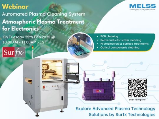
Webinar: Explore Advanced Plasma Technology Solutions by Surfx Technologies On Tuesday 25th February 2025 @ 10.00am - 11.00am
Join an insightful webinar hosted by Surfx Technologies and MELSS where we dive into the world of atmospheric plasma systems, offering cutting-edge solutions for high-volume manufacturing. In this session, we’ll explore how our innovative plasma technology can enhance surface treatments, improve adhesion, and ensure high-quality results in a variety of industries, including semiconductor packaging, electronics assembly, aerospace, and medical devices.
Registration Link: https://zurl.co/UZ2B7
0 notes
Text
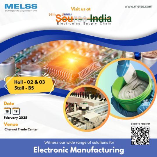
Witness our wide range of solutions for Electronic Manufacturing at Source India 2025. Visit us at Hall No.02 & 03 | Stall No. B5 on Feb 18th & 19th at Chennai Trade Center.
0 notes