#electrodeposit
Text
Developing a new system based on thermogalvanic effect to make mirror polishing easy, to save myself time with Bath interferometer in hand.
Easy to see how it can be generalized to parabolic + spherical mirror with parabolic focus at spherical center mirror doublet, and to many more applications where zero astigmatism is desired, but you don't want to spend a month polishing this shit.

4 notes
·
View notes
Text
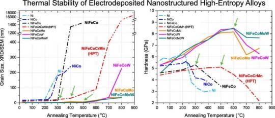
Researchers establish commercially viable process for manufacturing with promising new class of metals
Nanostructured high entropy alloys—metals made from a chaotic mix of several different elements—show a lot of promise for use in industries such as aerospace and automotive because of their strength and stability at high temperatures compared with regular metals.
But they are expensive and energy-intensive to produce. Now, researchers working with the Canadian Light Source (CLS) at the University of Saskatchewan (USask) have found a much cheaper and easier way to make them, opening the door for commercial applications.
Michel Haché, a materials engineer at the University of Toronto, and colleagues confirmed that electrodeposition is a cost-effective and easily scaled way to create these alloys. Electrodeposition—which involves dissolving metal ions in water and then using an electric current to pull them out of the liquid and form solid materials—is the same process that is used to make chrome-plated motorcycle parts. The findings are published in the journal Surface and Coatings Technology.
Read more.
#Materials Science#Science#Metals#High entropy alloys#Alloys#High entropy materials#Materials processing
16 notes
·
View notes
Text
Computational design on the Biorock Pavilion:
Excerpt from Dezeen article:
The Biorock Pavilion is a concept for an amphitheatre-like event space that could be grown underwater. The form of the building is based on that of a seashell, as well as mathematical forms.
The basis of the pavilion would be a skeletal structure comprised of a network of very thin steel rods, which would be immersed in a solution of minerals.
It would be grown by electrodeposition of minerals
An electric current would then be run through the steel skeleton, allowing the remainder of the pavilion to be 'grown' as the minerals calcify atop the base structure.
"It takes those minerals out of the seawater and produces a structure similar to reinforced concrete," stated Pawlyn. "This uses an absolute minimum of material to grow a whole building."
#biomimicry#biodesign#bio inspired#ecopunk#solarpunk#architecture#sustainable development#sustainable design#computational design#sustainable architecture#Michael Pawlyn#lol if you saw me accidentally post this on my studyblr no you didn't
41 notes
·
View notes
Text

ELEANOR MOTY
Choker in Plexiglas, quartz crystal with inclusions of moss agate, sterling silver, photo-etched sterling silver image, fine silver electrodeposition. Designed and made by Eleanor Moty, USA, 1972. (x)
2" H X 6" D
4 notes
·
View notes
Text
I went down a few rabbit holes while researching the Advent Calendar last year, that didn't make it into the queue because they got too long or went too far afield. Here's one of them!
One thing you notice when you watch a bazillion videos about old games consoles is how the design of circuitry has evolved. If someone says 'circuit board' today, you think a light piece of leafy green board, filled with parallel lines of copper at 45° and 90° angles, dotted with lots of tiny inscrutable plastic and metal doodads. But it took a long, long time for them to get that way.
If you look at really old circuit boards -- and I mean really, really old circuit boards, like from the beginning of the transistor era, they look completely different. They're brownish, for one thing. And kind of... wiggly?
youtube
Apologies for the transfer quality. It's not your connection, it just sucks. This piece appears to be some sort of promo-tainment thing from Tektronix themselves, from 1969. The rounded corners and bluish fuzz at the edges is an effect called 'vignetting', and it means this is originally from a 16mm film reel. There's no earthly reason for film to look this terrible. The uncentered picture means someone copied it by pointing a camera at a projection screen instead of bothering to get a proper kinescope setup, and the fact that it only goes up to 240p makes me feel like it was originally transferred over two decades ago for RealPlayer and nobody bothered to fix it for YouTube. VHS is about 240 lines, but if this were a crap transfer from a VHS tape you'd also see scanlines. It's possible there's a better copy at VintageTek, a museum dedicated to the history of Tektronix; they are an all-volunteer institution, and they probably have more important things to funnel funding to than updating their YouTube channel.
Point being, it looks like porridge and I'm sorry, but at least the content is interesting.
The brownish color, which is actually from an evolutionary stage earlier than what's covered here, is because many early boards were milled of bakelite rather than electrodeposited onto a glass or fiberglas backplane. If you want to see some of what that might have been like, you can hop over to Usagi Electric. He uses CAD to mill boards, rather than the photochemical process described by Tektronix, but it's pretty much the same idea. He does a lot of it in pursuit of his mad obsession with building a vacuum tube computer here. (If you're curious, his logo says うさぎ電気, "Usagi Denki". "Usagi" is Japanese for rabbit or bunny -- there is one who appears at the end of some videos -- and the spelling of "denki" here specifically means electrics, as opposed to 電機, which is usually rendered electronics. It still pops up in the names of some engineering or technology firms, but generally only the really old ones.)
The wiggly nature of early boards is neatly explained by watching the drafting process, starting about three minutes into the video. It was originally done by hand. The rest of the half-hour video goes through the whole multi-stage process, but the gist is that when you lay out the board, you draw dark lines where you want the conductive traces to be on the final product. To get a consistent size, tape is used for "holes" and tape lines are uses for the traces. If you've ever used stripe tape in nail art, it was apparently something like that -- vinyl tape with a bit of stretch, so you could curve it around. It was a methodical sort of art form. Ever solved one of those "connect the same-color dots without crossing lines" puzzles? It's basically that. If you can't find a topologically-appropriate solution on a single plane, you can produce boards with traces on both the front and the back, as Tektronix does here, and these days you can actually bury traces in internal layers as well. It's just a pain and makes the cost go up exponentially.
The mention of "holes" is interesting. Early circuit boards were nothing but holes. Everything had legs and was soldered on from the underside. Today these are known as "through-hole mounted" components; the alternatives are "surface-mount" components, which are generally smaller and fiddlier to solder on by hand, but considerably easier to lay down and solder in place by machine. Surface-mount technology has been around since before this Tektronix piece, but remained NASA-grade esoterica until the automated assembly process became cost-effective in the 1990s. Today the conductive holes are referred to as "vias" and the little medal dots surface-mount things are soldered to are "pads".
I'll also note that they show the automatic soldering process for these boards late in the video. It involves skimming the boards across the surface of a pool of molten solder. Solder in the 1960s contained a lot of lead. I would not personally like to be in that room. Today a machine places little surface-mount doojiggers in place along with solder beads, and then melts it all very gently in a very hot oven until it all melds together, not unlike a pan of slightly too-runny cookies. If you do it right, the surface tension of the solder keeps it on the pads and out of the traces. This is particularly useful for placing CPUs, whose myriad tiny pins in a tight grid would be far too difficult to solder by hand, and the origin of "reflow" repairs for electronics that are exhibiting symptoms of flaky solder joints.
The "silkscreening" process here does not use silk, but originally it did -- it was invented in Asia, logically enough. The gist of it is that you take a piece of finely woven mesh, traditionally light silk but in modern times also metal or synthetic fiber, and you plug up all of the little holes in it in the areas where you don't want ink to get through it, usually with some sort of water-repellent substance. In the days of yore, you painted on some kind of sap or wax, but nowadays it's usually a light-sensitive plastic that's scraped across the whole mesh, topped with a stencil that is opaque where you want ink to flow, and exposed to UV light that sets the substance. The unset areas that were in shadow are rinsed clean, leaving the mesh permeable in those places. The ink emulsion is then applied to the printing surface beneath in the reverse process: Ink is spread across the mesh, then squeegeed through with enough force to push it through the holes in the weave and onto the surface beneath. The dots of ink bleed just enough to flow into one another, producing a solid area of pigment. The circuit board designs were originally drafted in black on a white background, then photographed and reduced to 1/4 their original size, and the film used as the stencil for the silkscreen.
Holes are drilled mostly by hand(!) in this clip, which is an error-prone process, as you can see from the Usagi Electrics guy. The worker uses what's called a pantograph drill. A pantograph is a device that translates motion from one place to another, often with a change in scale. Typically pantographs are mechanical in nature, based on the complimentary motion of opposite corners of a parallelogram, but you could make a pretty good argument that modern systems that accept movement inputs from a user and translate them elsewhere by computer are also members of the class. Robot-assisted surgery comes to mind. If you cared to have an even longer argument, you could also consider systems that scan items with laser photons in order to reproduce them on a lathe or CNC machine pantographs in spirit, if not in fact.
A visual or optical comparator is just a device that projects a magnified view of something up on a screen, along with a point, grid, or profile it needs to match, not unlike a microfiche viewer with a targeting reticule. They're still used in some areas, although software image processing is steadily gaining ground.
You'd be amazed at how many things still need a look-over by a human with a brain. The lack of human brains is how we got the sharply-angled board traces we have today, in fact. Computer-aided drafting was developed to a usable level in the 1980s, and predictably the people using it were mostly engineers. The kind of route-finding you do in those connect-the-dots puzzles, and that the electronics engineers did when drafting the boards, is one of those very slippery human things. You want to find the shortest path, to save on the precious metals you use as conductors, but the absolute shortest path (with reasonable tolerances) is often a very snaky curve that would require a large number of points to define. It's much simpler to work on a grid, hence the 45° and 90° angles -- this ensures that all trace paths can be defined exclusively by where their corners lie on a square coordinate system, and is much less calculation-intensive. This was a lot of what early graphics tablets (or digitizers) were used for, and some light pen systems.
Having watched my father do a lot of this as a kid, I gather that at least in modern CAD software, you can just pick things up and put them wherever you want, but that the autopathing gets very confused if you do it too much -- mostly it's better to let the computer figure out where the traces go and tell you if you want something impossible in 3D space. And if you screw up anyway, there's always blue wire.
Circuit boards don't have to be the ubiquitous green, either. That's just the color of the solder mask, a lacquer painted all over the parts of the board you don't want solder to stick to. It's mostly tradition at this point, but you can get boards in pretty much any color you like -- the second most common I've see is a dark navy blue, probably because copper traces and white silkscreening stand out best on those two colors. You're welcome to get neon purple, if you can find anyone offering it.
from Blogger https://ift.tt/wicV2vP
via IFTTT
--------------------
Enjoy my writing? Consider becoming a Patron, subscribing via Kindle, or just toss a little something in my tip jar. Thanks!
7 notes
·
View notes
Text

SUBJECT
Electrodeposition of Pore-Confined Molybdenum Sulfide in Metal-Organic Framework Thin Films for Hydrogen Evolution Reaction
DEPARTMENT
Department of Chemical Engineering
PROFESSOR AND STUDENT
Professor:Chung-Wei Kung
Student:YOU-LIANG,CHEN
ABSTRACT
本研究把以鋯為基底的金屬有機骨架(Metal-Organic Framework, MOF)薄膜生長在導電基板上,並以週期性間歇定電流法在電鍍液中將硫化鉬電鍍在具有MOF的導電基板上。���MOF不具導電性且孔洞互相連通,故電鍍後可得被孔洞侷限、高表面積的硫化鉬。由於硫化鉬可電催化水還原,預期此電極材料將具備優異的催化產氫效率。由實驗結果可知,電鍍後的MOF結晶性完好但無法有效提升硫化鉬的催化產氫效率,推測是硫化鉬前驅物難以進入MOF的孔洞中。因此本研究將轉換合成法以增加催化劑表面積,先以Solvothermal deposition in MOF (SIM)法將鈷離子鍵結在Zr-MOF的節點之上,接著進行硫化將節點上的鈷離子轉化成硫化鈷奈米粒子並侷限在MOF的孔洞中,此法將可得侷限在PCN-222孔洞中具高比表面積的硫化鈷奈米粒子,而此硫化鈷奈米粒子預期可進一步提高硫化鈷的催化活性。
Original URL: 03-Stud:Department of Chemical Eng【YOU-LIANG,CHEN】-Undergraduate Research , NCKU https://en.ur.ncku.edu.tw/book/03-Stud:Department+of+Chemical+Eng%E3%80%90YOU-LIANG,CHEN%E3%80%91/
The copyright belongs to the author. For commercial reprints, please contact the author for authorization, and for non-commercial reprints, please indicate the source.
2 notes
·
View notes
Text
0 notes
Text
D'oh! Should've focused on understanding ion and molecular solvation behavior in electrolytes as a gateway to control electrochemical processes such as metal electrodeposition, ion intercalation, and electrocatalytic conversion...
1 note
·
View note
Text
0 notes
Text
What we need are smart windows
These windows take a lot of time to switch from one transparency level to another, and it is difficult to colour tune this material as desired. This problem is more prevalent in office buildings as people spend most of their time on computer screens. Excess of light also means more heat, and consequently increased energy consumption as air-conditioners stay on longer. Some-times, we face glare due to too much daylight which makes it difficult to perform tasks such as reading and typing on screens, which reduces productivity.Another important feature of this technique is that it uses only 20nm of metal for getting complete opacity.
Such windows will filter out all wavelengths equally and will provide the uniform colour of daylight.The presently available smart window solution employs electrochromic technology that provides dynamic tinting of glass by either automatic or manual control. Natural light impacts the visual quality of a space and also thermal needs of occupants. The lab prototype of this window contains a Cu-Ag gel electrolyte instead of liquid because it is less prone to leaks, has easier fabrication process and keeps the electrolyte confined in case of any accident. They will block up to 90 per cent of the light, reducing glare and heat while facilitating the outdoor views.Researchers at Stanford University have recently developed a smart window with a completely different approach.
What we need are smart windows that can adapt to the outdoor environment and provide comfort to the occupants of buildings, while also saving energy. Their prototype is based on reversible metal electrodeposition of Copper-Lead or Copper-Silver on a transparent conducting electrode that switches uniformly between transparent and opaque states in less than three minutes. Although several companies are trying to commercialise electrochromic windows, this technology is expensive. Many studies have shown that the visual and thermal comfort factors affect China Automation Components the productivity of occupants. As the metals have reflective properties, this technique works better in heat management than the electrochromic materials. Smart windows based on reversible metal electrodeposition exhibit fast switching times, high durability, tuneable transparency and chemical stability. Further, they manage heat poorly because they re-radiate the absorbed light as heat and their life is comparatively short due to degradation at each on/off cycle.India has abundant amount of daylight, and new technologies in smart windows such as technology based on reversible metal electrodeposition might be a possible solution.Current market solutions to overcome these issues are window shades such as curtains and interior blinds. They also help in energy conservation by bringing in natural light and thereby reducing the need for electric lighting.
Natural light changes throughout the day. Recent studies show that smart windows can reduce energy consumption for lighting and cooling up to 20 per cent by controlling the entry of daylight.A new technology makes glass provide uniform colour of daylight, reduce glare and heat while maintaining outside view. However, they cannot meet the two objectives simultaneously: maintaining the outside view and controlling the amount of daylight entering the space according to the changing outdoor environment.(The writer is a Professor in Building Science, IIIT, Hyderabad).Windows provide a soft transition between interior and exterior spaces by allowing daylight, ventilation and outside views essential for occupants’ well being.At present such windows are used in airplanes and luxury cars and are seldom used in buildings. Therefore, it can be commercialised more easily.As compared to the electrochromic window, they can go up to more than 5,000 cycles of switching with minimum degradation and thus are more durable.The key to uniform reversible metal deposition is nucleation of metal on ITO electrode surface by using platinum nano particles.
0 notes
Text
0 notes
Text
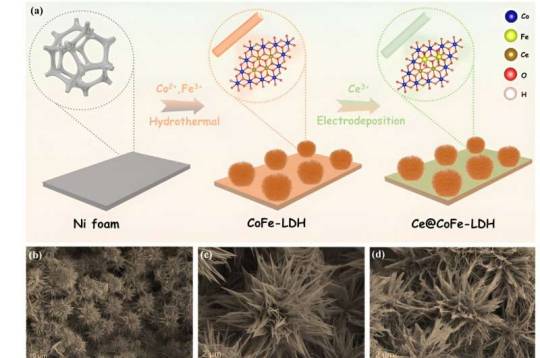
Urchin-like CoFe-layered double hydroxide synthesized for high-efficiency electrocatalytic oxygen evolution
A research team led by Professor Wang Qi from Hefei Institutes of Physical Science, Chinese Academy of Sciences, has successfully synthesized a heterogeneous Ce@CoFe-LDH electrocatalyst by combining a simple hydrothermal method with rapid electrodeposition.
The results were published in Inorganic Chemistry Frontiers.
Electrochemical water splitting is vital for clean hydrogen energy production. The oxygen evolution reaction (OER) in water splitting is slow due to complex electron transfer steps. Noble metal-based nanomaterials like Ru or Ir are effective OER catalysts but face scarcity and stability issues. Developing stable OER electrocatalysts based on transition metals is crucial for large-scale applications.
Read more.
6 notes
·
View notes
Text
Electroplating in Sharjah
Many products we use primarily indoors or in a dry setting for decorative purposes where they are unlikely to suffer from corrosion. Without losing the original metallic effect, these items are chemically coated with a thin layer of nickel, gold, silver, antique, etc. to make them attractive to the consumer. This layer is known as electroplating and is renowned for corrosion and rust prevention. The most common use of our electro-plating components is in malls, branded shops, hotels, Interior decorations, Fit-Outs, jewelry, Sheets, Claddings, HandRails, Frames, Corners, Skirtings, Stands, Channels, Profiles, etc. Our signature decorative items featured with different kinds of electroplating make us a well-known brand.
Classic Metal Coating provides optimally integrated processes in order to meet the exceptionally high-quality standards for decorative surfaces, where even the slightest amount of contamination contributes to defects. In terms of overall process costs, these systems are environmentally sustainable and streamlined.
Breaking Barriers in Electroplating: Emerging Trends and Techniques
Electroplating, also known as electrodeposition or electroplated coating, coats metal with a thin layer of another metal using electrolysis. It strengthens the metal’s corrosion resistance. Electroplating alters physical characteristics. The alteration in physical characteristics improves aesthetics, corrosion prevention, and wear resistance. Electroplating improves metal beauty, special surface, engineering, and mechanical qualities. Electroplating in UAE uses copper, nickel, gold, silver, chrome, zinc, tin, rhodium, and aluminium most often.
What is Electroplating?
Electroplating is the mechanism by which an electro-deposition is applied to another piece of metal (or to another conductive surface) using an energy current. The deposited metal becomes part of the current product in electroplating through plating/coating.
For electroplating a metal, it needs to generate an electric current with two different metals, an electrolyte solution, two electrodes, and battery or other energy.
Electroplating usually offers a more luxurious finish to cheaper metals and adds certain properties such as anti-corrosion and anti-rust.
#gold plating in dubai#metal coating companies in dubai#silver plating in uae#copper plating in uae#metal coating companies in sharjah#nickel & chrome plating in uae#brass plating in uae#electroplating companies in uae#electroplating in uae#gold plating in ajman
0 notes
Text
Copper Foil Market - From Supply Chain Resilience to Technological Advancements
The global copper foil market size is anticipated to reach USD 22.00 billion by 2030 and is anticipated to expand at a CAGR of 11.9% during the forecast period, according to a new report by Grand View Research, Inc. Increasing adoption of renewable energy sources and electric vehicles (EVs), as a part of decarbonization efforts, is projected to fuel the growth of global market for copper foil. Copper foil functions as the electrical conductor of printed circuit board (PCB). Rising demand for PCBs, due to the aforementioned application of copper foil in them, is likely to play a crucial role in influencing demand for copper foil. PCBs are essential building blocks in electronics manufacturing. As electronic devices become more complex and intelligent, there is an ever-growing demand for PCBs. As a result, rising demand for smart devices is likely to propel growth of the industry.
Copper Foil Market Report Highlights
Based on product, rolled foil held a maximum revenue share of over 55.0% in 2023 and is expected to grow at a significant CAGR over the forecast period due to its high consumption in batteries, solar panels, and IoT-enabled services, among others
Based on application, batteries segment is expected to grow at a lucrative pace over the forecast period owing to the growing EV industry
In solar & alternative energy, tin-plated copper foils in combination with acrylic-based pressure-sensitive adhesive tapes, are used in thin-film solar applications. These are solderable, and their usage provides stable electrical performance and is also easy to work with during the solar panel production process
Asia Pacific dominated the market owing to several countries in region focusing on reducing their carbon emissions by shifting their attention toward the adoption of renewable energy. For instance, according to the International Trade Administration, Taiwan plans to cater to 20% of its energy requirements from renewable sources by 2025. It is expected to harness 20 GW of solar energy by 2025
In January 2024, Hungary-based Volta Energy Solutions announced its geographic expansion into North American market by building a new battery copper foils plant in Quebec, Canada to cater to a fast-growing EV segment. It is a developer of world's first electrodeposited copper foils for batteries
For More Details or Sample Copy please visit link @: Copper Foil Market Report
Use of copper results in reduced carbon emissions and cuts down amount of energy required to generate electricity. There is six times more copper in renewable energy systems than in traditional systems. Hence, growing adoption and transition towards green energy in infrastructure development, such as electric vehicles (EVs) and electricity generation is anticipated to benefit market growth. According to the IEA, the global sales of EVs reached 10.3 million units in 2022 compared to 6.7 million units in 2021 and 3.2 million units in 2020. Global sales are expected to have touched 14.1 million units in 2023; however, actual statistics are yet to be published.
Copper is a commodity that has historically witnessed high price volatility during the historic period of 2018-2022. Fluctuations in prices of copper cathode are expected to have a bearing on the profitability of the producer. Further, hikes in energy prices, supply constraints, and high demand from end-use industries are expected to put pricing pressure on the global market and affect smelter profitability and revenue performances of foil producers over the forecast period. Hence, price volatility of copper is expected to be a significant restraint to the revenue performance of the market.
The market is very competitive, with a strong presence of several large-sized players, such as Nippon Denkai, Ltd., SKC, and Lotte Energy Materials Corporation. Due to growth of end-use applications, players have been investing in increasing their capacities through greenfield projects. For instance, in August 2023, Lotte Energy Materials Corporation announced that it would build a new foil plant in Spain and would be operational in 2025.
#CopperFoilMarket#Electronics#ConductiveMaterials#Manufacturing#Technology#RenewableEnergy#ElectricVehicles#Semiconductors#SupplyChain#Sustainability
0 notes
Text
Copper Foil Market Focusing On The Basis Of Product, Application, Region And Forecast 2030: Grand View Research Inc.
San Francisco, 16 April 2024: The Report Copper Foil Market Size, Share & Trends Analysis Report By Product (Electrodeposited, Rolled), By Application (Circuit Boards, Batteries, Solar & Alternative Energy, Medical), By Region, And Segment Forecasts, 2024 – 2030
The global copper foil market size is anticipated to reach USD 22.00 billion by 2030 and is anticipated to expand at a CAGR of 11.9%…

View On WordPress
0 notes
Last Seen Blogs

blacc-ikon
Araciel

fuckyeahpipesofpan
Pipes of Pan

dokidobe
yellow.dr.monv

jelly78
Unbetitelt

rietveldz
rietveldz