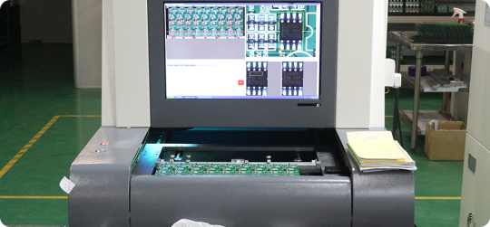
#led epitaxial wafer
Text
Epitaxial Wafer Market Trends Growth by Innovation in LED lighting
The epitaxial wafer market plays a pivotal role in manufacturing high-performance semiconductor devices used in applications ranging from consumer electronics to advanced healthcare devices. Epitaxial wafers aid in developing sophisticated integrated circuits and semiconductor chips through epitaxial growth techniques. Advancements in LED technology have increased the demand for epitaxial wafers for commercial and industrial applications. The global epitaxial wafer market is expected to gain significant traction on account of rising adoption of LED lighting and displays.
The Epitaxial Wafer Market size was valued at USD 2,778 million in 2022 and is anticipated to witness a compound annual growth rate (CAGR) of 12.9% from 2022 to 2030.
Key players operating in the epitaxial wafer market are EpiWorks Inc., Global Wafers Japan Co. Ltd., Nichia Corporation, SHOWA DENKO K.K., Siltronic AG, Desert Silicon Inc., Electronics and Materials Corporation Ltd. Intelligent Epitaxy Technology Inc.IQE plc., Jenoptic AG, MOSPEC Semiconductor Corporation, Norstel AB, Ommic S.A., Silicon Valley Microelectronics Inc., SVT Associates Inc. Universal Wafer Inc., Wafer Works Corporation, Xiamen Powerway Advanced Materials Co. Ltd., and Visual Photonics Epitaxy Co. Ltd.
Key Takeaways
Key players: EpiWorks, Global Wafers Japan, and Nichia captured over 35% share of the global market in 2024. EpiWorks leads the market with its diversified product portfolio and strong customer base.
Growing demand: Rising adoption of LED lighting, increasing penetration of advanced displays in consumer electronics and mobile devices, and growth of the semiconductor industry will continue to boost demand for epitaxial wafers in the coming years.
Global expansion: Leading manufacturers are investing heavily in capacity expansion plans across China, Taiwan, Europe, and the US to cater to the growing worldwide demand. Strategic partnerships and joint ventures are also gaining traction.
Market key trends
The Epitaxial Wafer Market Trends is undergoing significant transformation led by technological innovation in LED lighting applications. Manufacturers are focusing on developing high-quality mono-epitaxial and multi-epitaxial wafers to enable the mass production of more energy-efficient LED bulbs, streetlights, lamps, and advanced display backlights. Additionally, continuous ramp-up in wafer sizes from 150mm to 200mm and above is helping chipmakers lower production costs and improve epitaxial growth yield. This shift towards larger and more advanced epitaxial wafer substrates will define future market trends.
Porter’s Analysis
Threat of new entrants: New companies find it difficult to enter this market as a significant capital investment and technical expertise is required to set up manufacturing facilities for epitaxial wafers.
Bargaining power of buyers: Large technology companies like Intel, TSMC, Samsung, etc have significant bargaining power over epitaxial wafer suppliers given their high purchase volumes.
Bargaining power of suppliers: The presence of many established players limits the bargaining power of suppliers in this market.
Threat of new substitutes: There are limited substitutes for epitaxial wafers as they enable performance and cost benefits for several semiconductor devices.
Competitive rivalry: The market is dominated by few global players who compete intensely on technology leadership, quality, and customer service.
Geographical Regions
Asia Pacific accounts for the major share of the global epitaxial wafer market in terms of value owing to presence of large semiconductor manufacturing facilities and foundries located in countries like China, Taiwan, South Korea and Japan.
North America is expected to witness the fastest growth during the forecast period due to expanding semiconductor industry and ongoing technological advancements in the region. Rising demand for advanced semiconductor devices from sectors such as consumer electronics, automotive, industrial will drive the epitaxial wafer market in this region.
Get more insights on Epitaxial Wafer Market
About Author:
Money Singh is a seasoned content writer with over four years of experience in the market research sector. Her expertise spans various industries, including food and beverages, biotechnology, chemical and materials, defense and aerospace, consumer goods, etc. (https://www.linkedin.com/in/money-singh-590844163)

#Coherent Market Insights#Epitaxial Wafer Market#Epitaxial Wafer#Semiconductor Wafer#Epitaxy#Silicon Wafer#Semiconductor Materials#Epitaxial Layer#Microelectronics
0 notes
Text
Over £1M for global semiconductor firm IQE to enable industrialisation of ULTRARAM

An Innovate UK project worth £1.1M has been awarded to the Lancaster University spinout firm Quinas, the global semiconductor company IQE and Lancaster and Cardiff Universities.
Quinas will coordinate the ambitious project which is the first step towards volume production of the universal computer memory ULTRARAM™ invented by Lancaster Physics Professor Manus Hayne.
ULTRARAM has extraordinary properties, combining the non-volatility of a data storage memory, like flash, with the speed, energy-efficiency, and endurance of a working memory, like DRAM.
Most of the funding for the one-year project will be spent at IQE which will scale up the manufacture of compound semiconductor layers from Lancaster University to an industrial process at the Cardiff based firm. This will involve IQE developing advanced capability for growth of the compound semiconductors gallium antimonide and aluminium antimonide for the first time. The project follows significant investment to boost the UK semiconductor industry and the establishment of the world’s first compound semiconductor cluster in South Wales.
Professor Hayne, who is the Lancaster team lead, co-founder and Chief Scientific Officer at Quinas said: “We are delighted that Innovate UK is supporting this ambitious project, and that IQE has committed to developing the first part of ULTRARAM mass production.”
It is estimated that the global memory chip market will be worth about US$320 billion by 2030 but the UK currently has no stake in it.
Professor Hayne said: “ULTRARAM represents a tremendous economic opportunity for the UK, and the efficiencies it could bring to computing at all scales has the potential for huge energy savings and carbon emission reduction.”
Jessica Wenmouth Lancaster University’s Head of Research Commercialisation said: “I am delighted to support our spinout Quinas on its journey to scale this Lancaster-led innovation to an industrial process suitable for a semiconductor foundry 'fab,’ thereby generating impact from research through commercialisation.
“This project not only aligns with Lancaster University's strategy to foster impactful research and innovation but also demonstrates the effective utilisation of strategic grant funding alongside private equity investment. Such collaborations are crucial for bringing new products to market and driving significant investment into the UK for emerging technologies, enhancing our national and global standing in cutting-edge fields.”
The goal of the one-year project to industrialise the process involves scaling up ULTRARAM wafer diameters from 3” at Lancaster to 6” at IQE. This will be achieved by using the mainstream production technique of metal-organic vapour phase epitaxy (MOVPE), also called metal-organic chemical vapour deposition (MOCVD), rather than molecular beam epitaxy (MBE), which is typically used at universities.
Professor Hayne said: “Lancaster will do some initial MBE epitaxy as a control/template for the industrial growth. Our key role will be to characterise the antimonide material grown at IQE, and once sufficient quality is confirmed we will fabricate and test ULTRARAM memory on small areas of the wafers from IQE.
“In parallel with this, Lancaster will continue to work on ULTRARAM scaling, by reducing the size of individual devices (‘Moore’s law’) and making larger and larger arrays. Once devices are small enough and arrays are large enough, the following stage will be to demonstrate fabrication on a complete 8” wafer, and then to translate the process to an industrial one, suitable for a semiconductor foundry ‘fab’.”
ULTRARAM exploits quantum resonant tunnelling to achieve its extraordinary properties and is implemented in compound semiconductors that are used in photonic devices such as LEDs, laser diodes and infrared detectors, but not in digital electronics, which is the preserve of silicon.
Story via lancaster.ac.uk
Read the full article
0 notes
Text
0 notes
Text
Unlocking the Power of High-Temperature Furnaces: Innovations and Applications
High-temperature furnaces stand as marvels of engineering, enabling the manipulation of materials at extreme temperatures for various industrial and scientific purposes. These furnaces, with their ability to reach temperatures exceeding 1000°C and even surpassing 3000°C in some cases, play a pivotal role in numerous fields, ranging from materials science and metallurgy to research and development. Let's delve into the intricacies of high-temperature furnaces, exploring their innovations, applications, and significance in modern industries.

Understanding High-Temperature Furnaces:
High-temperature furnaces are specialized heating devices designed to subject materials to intense heat, enabling processes such as sintering, annealing, melting, and heat treatment. They utilize advanced heating elements, insulation materials, and control systems to achieve and maintain precise temperature conditions. These furnaces can operate under various atmospheres, including vacuum, inert gas, and controlled atmospheres, allowing for tailored thermal treatments to suit specific materials and applications.
Innovations Driving Performance:
Recent advancements in materials science and furnace technology have led to significant improvements in the performance and capabilities of high-temperature furnaces. Innovations such as refractory materials with enhanced thermal stability, advanced insulation techniques to minimize heat loss, and sophisticated heating elements capable of rapid heating and precise temperature control have revolutionized the functionality of these furnaces. Additionally, the integration of automation and digital control systems has enabled greater efficiency, repeatability, and flexibility in furnace operation.
Applications Across Industries:
The versatility of high-temperature furnaces renders them indispensable across various industries, where thermal processing plays a critical role in materials synthesis, fabrication, and characterization. Some key applications include:
Metallurgy and Materials Science: High-temperature furnaces are extensively used in metallurgical processes such as alloy production, heat treatment, and powder metallurgy. They facilitate the sintering of ceramics, annealing of metals, and diffusion bonding of materials, enabling the development of advanced alloys and engineered materials with tailored properties.
Semiconductor Manufacturing: In the semiconductor industry, high-temperature furnaces are employed for processes like epitaxial growth, oxidation, and diffusion of dopants in silicon wafers. These furnaces ensure precise control over temperature profiles and gas environments, crucial for achieving desired thin-film properties and device performance.
Glass and Ceramics Production: Glass melting furnaces and ceramic kilns utilize high temperatures to melt raw materials and shape them into desired forms. These furnaces play a vital role in the production of glassware, ceramics, refractories, and specialized materials used in construction, electronics, and aerospace industries.
Research and Development: High-temperature furnaces serve as indispensable tools in research laboratories and academic institutions, supporting a wide range of studies in materials science, chemistry, and physics. They enable experiments such as crystal growth, phase transformations, and thermal analysis, providing insights into material behavior under extreme conditions.
Future Prospects and Challenges:
As industries continue to push the boundaries of materials performance and functionality, the demand for high-temperature furnaces will likely escalate. Future developments may focus on enhancing energy efficiency, reducing environmental impact, and expanding the operational range of these furnaces to accommodate novel materials and processes. Challenges such as thermal management, material compatibility, and scalability remain areas of active research and innovation.
In conclusion, high-temperature furnaces stand as indispensable tools driving innovation and progress across diverse industries. Their ability to manipulate materials at extreme temperatures unlocks a realm of possibilities for material synthesis, processing, and characterization, paving the way for advancements in technology, manufacturing, and scientific discovery. As research and development efforts continue to evolve, high-temperature furnaces will remain at the forefront of thermal processing technologies, shaping the future of materials science and engineering.
0 notes
Text
Material and Manufacturing Improvements Enhance LED Efficiency
In theory, making high-brightness LEDs is easy. Just glue together n- and p-type semiconductors, add a small bias voltage, and stand back while the photons stream out. However, in practice these solid-state light sources are anything but simple. Advanced materials and manufacturing processes have come together to produce exotic devices with light outputs that would have been considered fanciful just half a decade ago.
Even though they produce impressive and highly efficient devices, the LED makers are not resting on their laurels. Leading LED companies such as Cree, OSRAM, and Seoul Semiconductor spend millions of dollars on material science and manufacturing technology to further enhance the performance of their products.
Contemporary high-brightness LEDs are already benefitting from advanced substrates and fabrication techniques, such as silicon carbide (SiC) and chemical vapor deposition (CVD), and tomorrow’s chips will take advantage of materials like patterned sapphire that are still percolating in the laboratory. This article takes a closer look at these materials and processes and assesses their impact on commercial LED performance.
Mind the band gap
Because the wavelength of the light emitted is a function of the energy band gap of the n- and p-doped semiconductor used to form the junction, engineers are limited in their choice of materials for fabricating LEDs. There is little point in selecting a semiconductor that emits photons that the eye cannot detect.
After many years of experimentation and hundreds of millions of research dollars, it turns out that Indium Gallium Nitride (InGaN) – a combination of Gallium Nitride (GaN) and Indium Nitride (InN) – is the best currently available semiconductor for high-brightness LEDs. The band gap of InGaN can be manipulated by altering the ratio of GaN to InN. The chips used at the heart of “white” LEDs, for example, emit photons in the 390 to 440 nanometer part of the spectrum (ultraviolet, violet-blue, and blue)1. These photons are then converted to white light by interaction with phosphor powder.
However, while InGaN has a number of advantages for photon generation, it does have some significant drawbacks from a volume manufacturing perspective. Chief among these is the fact that it is very difficult (and hence expensive) to “grow” InGaN ingots (unlike the silicon used for manufacturing integrated circuits (IC)). Ingots are advantageous for mass production because they can be sliced and processed as large wafers leading to lower cost chips.
Instead, manufacturers typically employ a much cheaper process whereby InGaN thin films are grown by a process known as epitaxy - the deposition of a crystalline overlayer on a crystalline substrate. There are several epitaxy techniques for forming the InGaN layer required for high-brightness LEDs, but the most common contemporary method is metal-organic CVD (MOCVD).
MOCVD is a complex process, but in basic terms, reactive gases are fed into a vacuum chamber and combine – at the atomic level – with the substrate and form a thin crystalline film.
During MOCVD, the crystalline structure of the deposited film attempts to orientate with the crystal structure of the substrate. The accuracy of this orientation depends on the similarity of the crystal lattice of each material. Poorly matched lattices result in a deposited film that while bulk crystalline on the macroscale is actually full of microscopic dislocations.
Reducing threading dislocations
A simplified schematic of the structure of a commercial high-brightness LED is shown in Figure 1.
The MOCVD process builds up the LED’s active regions – the multiple layers sandwiched between the p- and n-contact – by depositing successive thin films typically on a sapphire substrate. Sapphire has a number of advantages as a substrate for LED production: it is relatively inexpensive; it is used as a substrate for ICs so manufacturing processes are well established; it is very hard and durable, and it is a good insulator.
But there are some drawbacks. One such drawback is the mismatch in the coefficient of thermal expansion between sapphire and InGaN that can lead to high stresses and cracking of the fabricated die. However, an even bigger drawback is the relatively large mismatch between the crystal lattice of InGaN and sapphire (Figure 2). The mismatch – of around 14.8 percent – results in microscopic flaws in the InGaN thin film known as threading dislocations (Figure 3).
Figure 2: Lattice mismatch between sapphire substrate and InGaN thin film creates threading dislocations. (Courtesy of Cree.)
Figure 3: Threading dislocations in InGaN substrate.
Threading dislocations are a challenge in the drive to improve LED efficacy because recombinations between electrons and holes that occur at such sites are primarily “nonradiative.” In other words, no visible photon is emitted. This is because the dislocations introduce extra band gaps beyond the one that the designer intended, and hence do not correspond to the energy differential that produces a photon with a wavelength in the visible part of the spectrum.
Alternatively, the energy emitted in the recombination is transferred by the emission of a “phonon”, a vibration introduced to the crystal lattice that adds nothing to the chip’s luminosity but does generate unwanted heat. Because of the mismatch with the sapphire substrate, InGaN suffers from many threading dislocations, exhibiting typical densities exceeding 108 per cm2 or more.2 Worse yet, threading dislocations increase in number as the LED ages, further compromising luminosity (see the TechZone article “Understanding the Cause of Fading in High-Brightness LEDs”).
The drive for greater efficiency
Because of its fabrication advantages, the majority of manufacturers have been prepared to accept the threading dislocation compromise that comes with sapphire while improving their products’ efficacy by focusing on other aspects of LED performance.
LEDs such as OSRAM’s OSLON SSL, for example, can produce up to 108 lm/W (at 350 mA), a state-of-the-art performance, while fabricated on a sapphire substrate. In fact, over 90 percent of today’s high-brightness LEDs from most of the leading manufacturers are fabricated on sapphire substrates.3
As the efficacy returns from improving the other aspects of a LED’s performance – such as carrier injection efficiency, photon extraction, and phosphor conversion efficiency – begin to diminish, LED makers are turning their attention to alternative substrates.
One of those alternatives is silicon carbide (SiC). Like sapphire, SiC can be produced in bulk using fairly standard semiconductor manufacturing techniques. It also has the added advantage of a coefficient of thermal expansion that’s similar to InGaN, limiting stress buildup and die cracking. The primary disadvantages are high cost and patented manufacturing processes that require the payment of licensing fees.
Cree, a leading U.S.-based LED lighting maker, has – perhaps not surprisingly considering it owns many of the manufacturing patents – championed the use of SiC substrates for LED fabrication. The major advantage the material has over sapphire is a lattice structure that's much more closely matched to InGaN. By using SiC, the lattice mismatch with InGaN is reduced to 3.4 percent.4 This close matching is still not sufficient to eliminate threading defects completely (Figure 4), although the defect density is considerably reduced – by at least one and sometimes two orders of magnitude lower than sapphire5 – dramatically decreasing the number of sights for nonradiative recombination, improving efficacy and prolonging the life of the LED by slowing the rate of fading.
1 note
·
View note
Text
LED Chip Market Analysis of Growth Trends for 2023-2030
Illuminating Innovation: A Deep Dive into the LED Chip Market
In the world of lighting technology, Light Emitting Diodes (LEDs) have emerged as a beacon of efficiency, sustainability, and versatility. At the heart of every LED luminaire lies a tiny yet powerful component known as the LED chip, driving the revolution in energy-efficient lighting solutions. Join us as we embark on an enlightening journey through the LED chip market, exploring its significance, innovations, and the transformative impact it holds for the future of illumination.
Understanding LED Chips
LED chips are semiconductor devices that emit light when an electric current passes through them. These tiny chips, typically just a few millimeters in size, are the building blocks of LED lighting systems, providing the essential light source for a wide range of applications. LED chips are engineered to produce specific colors and intensities of light, making them highly versatile and adaptable to various lighting requirements, from general illumination to specialty applications such as automotive lighting, horticulture, and display technology.
Request Sample Report: https://www.snsinsider.com/sample-request/3199
The Significance of LED Chips
In an era marked by growing energy consumption, environmental concerns, and the push for sustainability, LED chips offer a compelling solution for reducing energy usage and carbon emissions in lighting. Compared to traditional incandescent and fluorescent lighting technologies, LED chips consume significantly less energy, last longer, and produce higher-quality light with superior color rendering and consistency. Moreover, LED chips are mercury-free and emit less heat, making them safer and more environmentally friendly than conventional lighting sources.
Innovations Driving Market Growth
The LED chip market is characterized by continuous innovation and rapid technological advancements, driven by the demand for higher efficiency, performance, and reliability. Innovations such as chip-on-board (COB) technology, phosphor conversion coatings, and micro-LEDs are pushing the boundaries of LED chip performance, enabling higher luminous efficacy, color accuracy, and design flexibility. Moreover, advancements in manufacturing processes, such as epitaxial growth techniques and wafer-scale packaging, are driving down production costs and improving the scalability and affordability of LED chips for mass-market adoption.
Applications Across Industries
LED chips find applications across a wide range of industries and sectors, from general lighting and automotive to signage, displays, and consumer electronics. In general lighting, LED chips are used in residential, commercial, and industrial luminaires to provide energy-efficient illumination for indoor and outdoor spaces. In automotive lighting, LED chips enable high-performance headlights, taillights, and interior lighting systems that enhance visibility, safety, and aesthetics. Moreover, in specialty applications such as horticulture lighting, UV disinfection, and wearable technology, LED chips offer tailored solutions to meet the unique requirements of each application.
Towards a Brighter Future
As we look to the future, the LED chip market holds immense potential for driving progress towards a more sustainable, energy-efficient, and connected world. By embracing the advantages of LED technology and investing in research, development, and innovation, we can unlock new opportunities for lighting design, human-centric lighting, and smart lighting solutions that enhance quality of life, productivity, and well-being. Moreover, as LED chips continue to evolve and diversify, they will play an increasingly important role in shaping the future of illumination, from smart cities and IoT-enabled environments to immersive entertainment experiences and beyond.
In conclusion, LED chips represent a shining example of innovation and sustainability in the lighting industry, offering a pathway towards a brighter, more efficient future for illumination. By harnessing the potential of LED technology and fostering collaboration between industry stakeholders, we can illuminate the path to a more sustainable and connected world. Let's embrace the possibilities of LED chips and light the way towards a brighter future for all.
Top of Form
Access Full Report Details: https://www.snsinsider.com/reports/led-chip-market-3199
0 notes
Text
Epitaxial Wafers Market Analysis, Dynamics, Players, Type, Applications, Trends, Regional Segmented, Outlook & Forecast till 2032
Epitaxial Wafers Market anticipated for USD 4.35 billion in 2023 and is estimated to be USD 13.04 billion by 2033 and is expected to register a CAGR of 11.6% during 2024-2033.
The competitive analysis of the Epitaxial Wafers Market offers a comprehensive examination of key market players. It encompasses detailed company profiles, insights into revenue distribution, innovations within their product portfolios, regional market presence, strategic development plans, pricing strategies, identified target markets, and immediate future initiatives of industry leaders. This section serves as a valuable resource for readers to understand the driving forces behind competition and what strategies can set them apart in capturing new target markets.
Market projections and forecasts are underpinned by extensive primary research, further validated through precise secondary research specific to the Epitaxial Wafers Market. Our research analysts have dedicated substantial time and effort to curate essential industry insights from key industry participants, including Original Equipment Manufacturers (OEMs), top-tier suppliers, distributors, and relevant government entities.
Receive the FREE Sample Report of Epitaxial Wafers Market Research Insights @ https://stringentdatalytics.com/sample-request/epitaxial-wafers-market/12567/
Market Segmentations:
Global Epitaxial Wafers Market: By Company
• EpiWorks(The US)
• Applied Materials(The US)
• GlobalWafers Co.(Taiwan)
• ASM International (The US)
• Hitachi Kokusai Electric Inc. (Japan)
• Tokyo Electron Limited (Japan)
• Nichia Corporation (Japan)
• AIXTRON SE (Germany)
• LamResearch Corporation(TheUS)
• Canon Anelva Corporation (Japan)
• IQE (The U.K.)
• Veeco Instruments(The US)
Global Epitaxial Wafers Market: By Type
• 50mm to 100mm
• 100mm to 150mm
• Above 150 mm
Global Epitaxial Wafers Market: By Application
• LED Semiconductor
• Power Semiconductor
• MEMS-based Devices
• Others
Regional Analysis of Global Epitaxial Wafers Market
All the regional segmentation has been studied based on recent and future trends, and the market is forecasted throughout the prediction period. The countries covered in the regional analysis of the Global Epitaxial Wafers market report are U.S., Canada, and Mexico in North America, Germany, France, U.K., Russia, Italy, Spain, Turkey, Netherlands, Switzerland, Belgium, and Rest of Europe in Europe, Singapore, Malaysia, Australia, Thailand, Indonesia, Philippines, China, Japan, India, South Korea, Rest of Asia-Pacific (APAC) in the Asia-Pacific (APAC), Saudi Arabia, U.A.E, South Africa, Egypt, Israel, Rest of Middle East and Africa (MEA) as a part of Middle East and Africa (MEA), and Argentina, Brazil, and Rest of South America as part of South America.
Click to Purchase Epitaxial Wafers Market Research Report @ https://stringentdatalytics.com/purchase/epitaxial-wafers-market/12567/
Key Report Highlights:
Key Market Participants: The report delves into the major stakeholders in the market, encompassing market players, suppliers of raw materials and equipment, end-users, traders, distributors, and more.
Comprehensive Company Profiles: Detailed company profiles are provided, offering insights into various aspects including production capacity, pricing, revenue, costs, gross margin, sales volume, sales revenue, consumption patterns, growth rates, import-export dynamics, supply chains, future strategic plans, and technological advancements. This comprehensive analysis draws from a dataset spanning 12 years and includes forecasts.
Market Growth Drivers: The report extensively examines the factors contributing to market growth, with a specific focus on elucidating the diverse categories of end-users within the market.
Data Segmentation: The data and information are presented in a structured manner, allowing for easy access by market player, geographical region, product type, application, and more. Furthermore, the report can be tailored to accommodate specific research requirements.
SWOT Analysis: A SWOT analysis of the market is included, offering an insightful evaluation of its Strengths, Weaknesses, Opportunities, and Threats.
Expert Insights: Concluding the report, it features insights and opinions from industry experts, providing valuable perspectives on the market landscape.
Report includes Competitor's Landscape:
➊ Major trends and growth projections by region and country
➋ Key winning strategies followed by the competitors
➌ Who are the key competitors in this industry?
➍ What shall be the potential of this industry over the forecast tenure?
➎ What are the factors propelling the demand for the Epitaxial Wafers?
➏ What are the opportunities that shall aid in significant proliferation of the market growth?
➐ What are the regional and country wise regulations that shall either hamper or boost the demand for Epitaxial Wafers?
➑ How has the covid-19 impacted the growth of the market?
➒ Has the supply chain disruption caused changes in the entire value chain?
Customization of the Report:
This report can be customized to meet the client’s requirements. Please connect with our sales team ([email protected]), who will ensure that you get a report that suits your needs. You can also get in touch with our executives on +1 346 666 6655 to share your research requirements.
About Stringent Datalytics
Stringent Datalytics offers both custom and syndicated market research reports. Custom market research reports are tailored to a specific client's needs and requirements. These reports provide unique insights into a particular industry or market segment and can help businesses make informed decisions about their strategies and operations.
Syndicated market research reports, on the other hand, are pre-existing reports that are available for purchase by multiple clients. These reports are often produced on a regular basis, such as annually or quarterly, and cover a broad range of industries and market segments. Syndicated reports provide clients with insights into industry trends, market sizes, and competitive landscapes. By offering both custom and syndicated reports, Stringent Datalytics can provide clients with a range of market research solutions that can be customized to their specific needs.
Reach US
Stringent Datalytics
+1 346 666 6655
Social Channels:
Linkedin | Facebook | Twitter | YouTube
0 notes
Text
Transformation and upgrading direction of LED display industry
Email: [email protected]
WhatsApp & Wechat: +86 18038197291
www.xygledscreen.com
In recent years, it can be seen from the products and businesses launched by screen enterprises that the entire industry has undergone a huge change: LED screen enterprises have changed from simple manufacturing and sales to comprehensive products. Such as smart all-in-one machine and other consumer market products that adapt to more commercial display scenes, command and scheduling solutions that are suitable for the construction of special display scenes, and application cases of "product+content production/creative design" in cultural and entertainment scenes. It can be seen that the tentacles of LED display industry have been extended outward.
The saturated professional market has given birth to new development needs
Throughout the development history of LED display, it is only 30 years. Before the 1990s, China's LED display industry was still in its infancy, and the products were mainly monochrome and red-green LED display products. After the 1990s, LED display entered the full-color period, and the LED display industry also ushered in a period of rapid development. The application field is gradually expanded and the industrial pattern is gradually improved. Especially after 2008, LED display screen has entered a new stage of development in terms of design concept, technical innovation, project scale, display effect, etc. In this process, there are also inevitable problems: the industry competition intensifies, and in order to seize the market, screen companies compete in price war. The quality of products on the market is also mixed, which also promotes the further implementation of industry norms and guidance. With the increase of production capacity and expansion of scale, the intensive development effect of the industry has become increasingly obvious. After more than 30 years of development, China's LED industry has formed a relatively complete industrial chain, including the production of epitaxial wafers, chip preparation and packaging, and the application of LED products.
For a long time, the development of LED display screen industry has been based on market demand, and technical research and development have been carried out on the display effect of products. The application field also has obvious characteristics: focusing on large-screen display, and focusing on the demand for information video display. With the increase of market demand, screen enterprises also continue to expand application scenarios and develop display application products in advertising media, transportation, sports, education, security and other markets. However, with the gradual saturation of the professional market, after a long period of market competition, the intensive trend of the screen enterprises is obvious, and the screen enterprises either integrate and merge, or create another market segment. After experiencing a series of internal and external factors transformation, in the gradually mature and saturated market, the competition between screen enterprises has become increasingly fierce, and gradually began to be unable to meet the needs of screen enterprises for further improvement and development. The development of the LED display industry is very similar to that of the large LCD screen market. At present, only a few leading enterprises in the LCD market are in a stagnant state of development in the quantitative share market, which also sounded a warning bell for the LED display market: when the traditional professional market has entered a saturation state, and the research and development of LED screen enterprises in the traditional product display technology can no longer rise, where should the screen enterprises go?
Try and adjust
In fact, from the development trend of LED display industry in recent years, we can see that screen enterprises are making new attempts and adjustments.
The shallowest attempt should be to transform module products into complete machine products and enter the commercial display market. In this attempt, the screen enterprise changed the original LED display screen from the video processor into the processor and display screen integrated into one product, and output the small spacing all-in-one machine product suitable for indoor use to the indoor display scene. This also means that LED display will not only compete with all kinds of splicing display products in the large screen market, but also compete for indoor display space in the field of commercial display, medium and large size display. LED screen enterprises follow a principle in product upgrading: how to make LED screen operation more convenient and convenient?
Perhaps inspired by information technology and digital products in recent years, combined with the development of 5G and other information technologies in recent years, the large display screen is no longer simply used as a display board of video materials, but the all-in-one machine products with software functions have been applied to various conference rooms, security monitoring, education fields and other places, and there are corresponding functional focus for the place, and even the product has achieved multi-function features, which can meet the needs of various application scenarios. Recently, LED all-in-one products are also emerging in an endless stream at major technology exhibitions. For large screen application scenarios such as the command center, various large screen enterprises have launched various integrated solutions. Thanks to the rising demand for digital upgrading of various scenes under the construction of smart cities, LED displays are given more market opportunities and market space. In fact, the smart all-in-one machine and the integrated solutions launched by various screen enterprises can also be regarded as an intelligent upgrade of screen products by screen enterprises, combining individual module discrete parts into a whole product, and matching the appropriate display operation software for consumer groups. This kind of product well meets the consumer's demand for simplified operation requirements of LED display, and becomes another competitive advantage of LED display products.
At the same time, screen enterprises also try to improve the added value of products and market competitiveness by "empowering" display products. In the market situation where the traditional LED display technology is maturing and the industry competition is becoming increasingly fierce, many screen enterprises have developed new business points in the application field, and "product+content production/creative design" has become the company's new business model. Relying on technological innovation, the product types of LED display are more diverse, and the combination with art design is more close, which creates more application space for the industry, but also challenges the display content of LED display with different appearances. This year, the trend of screen enterprises to layout the digital content sector is obvious. Many screen enterprises have developed digital content scene building businesses, including XR virtual digital people, virtual venues, virtual live broadcasting, bare-eye 3D and other digital content services. It also provides digital content design and production for the combination of various special-shaped displays and modern decoration, landscape and lighting in the bar, stage, art exhibition hall and other application scenarios to create more beautiful creative display application cases. LED display enterprises located in the professional field obviously know more about product characteristics, which also provides convenience for display enterprises to enter the digital content production market.
The evolution of the market and products has pushed the distance between screen enterprises and consumers closer. The market demand for LED display products has changed from rigid video information display to more flexible and unknown. With the development of Internet information technology, information dissemination is becoming more and more developed, LED display screens are no longer half understood by consumers, and the requirements for LED display products will be more stringent. However, the original market has become too saturated and the competition is fierce. In order to open up new markets and take the lead, enterprises must open up new LED display application roads, learn more "skills" and increase the "attribute value" of products.
0 notes
Text
Epitaxial Wafer Market Is Estimated To Witness High Growth Owing To Technological Advancements and Increasing Demand for Efficient Electronic Devices

The global Epitaxial Wafer Market is estimated to be valued at US$ 2,778 million in 2022 and is expected to exhibit a CAGR of 12.9% over the forecast period 2022-2030.
A) Market Overview:
Epitaxial wafers are single-crystal semiconductor wafers that are widely used in the production of integrated circuits and electronic devices. These wafers enable the growth of high-quality thin films with controlled crystal orientation, essential for the fabrication of various devices such as power devices, LEDs, and optoelectronic components. Epitaxial wafers offer several advantages, including improved performance and reliability of electronic devices, reduced power consumption, and smaller form factors. The increasing demand for efficient electronic devices and the continuous advancements in semiconductor technology are expected to drive the growth of the epitaxial wafer market.
B) Market Dynamics:
1. Technological Advancements: The Epitaxial wafers Market Demand is witnessing significant technological advancements, leading to the development of new and innovative products. For instance, companies are focusing on the development of high-quality epitaxial wafers with improved material properties, such as reduced defect density, higher carrier mobility, and enhanced light-emitting efficiency. These advancements are expected to drive the adoption of epitaxial wafers in various applications, thereby fueling market growth.
2. Increasing Demand for Efficient Electronic Devices: With the rapid advancements in technology, there is a growing demand for electronic devices that are more efficient, compact, and high-performing. Epitaxial wafers play a crucial role in the production of such devices by enabling the growth of high-quality thin films. The increasing adoption of smartphones, tablets, wearables, and other electronic devices is expected to boost the demand for epitaxial wafers.
C) SWOT Analysis:
Strengths:
1. High-quality Thin Films: Epitaxial wafers enable the growth of high-quality thin films with improved material properties, such as reduced defect density and enhanced carrier mobility.
2. Growing Semiconductor Industry: The rapid growth of the semiconductor industry is driving the demand for epitaxial wafers as they are an essential component in the production of integrated circuits.
Weaknesses:
1. High Cost: Epitaxial wafers Market Demand are relatively expensive compared to other semiconductor materials, which may limit their adoption in price-sensitive markets.
2. Complex Manufacturing Process: The manufacturing process of epitaxial wafers is complex and requires specialized equipment and expertise, which may pose challenges for new market entrants.
Opportunities:
1. Increasing Demand for Power Devices: The increasing adoption of power devices in various applications, including automotive, renewable energy, and industrial sectors, is expected to create lucrative opportunities for the epitaxial wafer market.
2. Emerging Technologies: The emergence of new technologies, such as 5G, Internet of Things (IoT), and artificial intelligence (AI), is expected to drive the demand for advanced electronic devices, thereby creating opportunities for the epitaxial wafer market.
Threats:
1. Intense Competition: The epitaxial wafer market is highly competitive, with several key players competing for market share. Intense competition may lead to price wars and profit margin pressures.
2. Trade Wars and Geopolitical Tensions: Global trade wars and geopolitical tensions can adversely impact the supply chain and disrupt the global epitaxial wafer market.
D) Key Takeaways:
- The global epitaxial wafer market is expected to witness high growth, exhibiting a CAGR of 12.9% over the forecast period, due to increasing technological advancements and the growing demand for efficient electronic devices.
- Asia-Pacific is expected to be the fastest-growing and dominating region in the epitaxial wafer market, driven by the presence of major semiconductor manufacturers and the increasing demand for consumer electronics.
- Key players operating in the global epitaxial wafer market include EpiWorks Inc., Global Wafers Japan Co. Ltd., Nichia Corporation, SHOWA DENKO K.K., and Siltronic AG, among others.
0 notes
Text
LED Bulb Raw Material Manufacturers: What You Need to Know
Lighting technology has come a long way over the years, and LED bulbs have taken center stage as one of the most energy-efficient and versatile options available. From their sleek design to their impressive lifespan, LED bulbs have revolutionized the way we illuminate our world. But have you ever wondered how these brilliant little lights are made? Behind every successful LED bulb is a team of talented engineers and manufacturers who work tirelessly to source high-quality raw materials. In this blog post, we will take a closer look at the leading LED bulb raw material manufacturer and uncover why opting for these innovative lighting solutions can be beneficial for both your pocketbook and the planet! So let's dive in and shed some light on what makes these manufacturers shine!
What are LED bulbs?
LED bulbs, or Light Emitting Diode bulbs, are a type of lighting technology that have gained immense popularity in recent years. Unlike traditional incandescent or fluorescent bulbs, LED bulbs use semiconductors to convert electricity into light. This means they consume significantly less energy and produce very little heat compared to their outdated counterparts.
The construction of an LED bulb is quite fascinating. At its core is a tiny chip made of semiconductor material that emits light when an electric current passes through it. The chip is housed within a lens or cover that helps direct the light output and protect the delicate components inside.
One of the key advantages of LED bulbs is their longevity. These marvels can last up to 25 times longer than traditional incandescent bulbs, which translates into fewer replacements and lower maintenance costs over time. Additionally, LEDs are known for their durability as they are resistant to shock and vibration.
Furthermore, LED bulbs offer tremendous flexibility in terms of color options and control capabilities. They can be manufactured to emit various hues without the need for filters or gels, making them ideal for creating dynamic lighting effects in commercial settings or even at home.
In addition to being environmentally friendly due to their low energy consumption, LED bulbs also contribute significantly towards reducing carbon dioxide emissions. Their efficiency leads to reduced demand on power plants resulting in decreased greenhouse gas emissions.
With all these incredible benefits packed into one small bulb package, it's no wonder why LED technology has become the go-to choice for both residential and commercial lighting needs! So let's continue our exploration by delving into who exactly crafts these remarkable innovations: the leading LED bulb raw material manufacturer
How are LED bulbs made?
LED bulbs are an incredible innovation that has revolutionized the lighting industry. But have you ever wondered how these amazing bulbs are made? Let's take a peek behind the scenes of LED bulb manufacturing.
The process starts with sourcing high-quality raw materials, such as semiconductors like gallium arsenide or gallium nitride. These materials form the basis for creating the light-emitting diodes (LEDs) inside the bulbs. Once obtained, they undergo precise purification techniques to ensure their purity and performance.
Next comes wafer production, where thin slices of semiconductor material are cut from ingots using advanced equipment. The wafers then go through several intricate processes like epitaxial growth, diffusion, and ion implantation to add various layers and dopants that determine their electrical properties.
Afterward, individual LEDs are created by adding electrodes and soldering them onto tiny chips on each wafer. This is followed by encapsulating each chip in a phosphor-filled epoxy resin to enhance light emission efficiency and color quality.
Once all the LEDs are prepared, they're carefully mounted onto a heat-conductive base or substrate using specialized adhesives or solders. This helps dissipate any excess heat generated during operation.
All components - including driver circuits for power regulation - are assembled within a protective housing to create a complete LED bulb ready for testing and packaging before being shipped out to consumers worldwide!
Intricate and precise steps make up the fascinating process of manufacturing LED bulbs. From sourcing raw materials to assembling complex circuitry into sleek designs – it's truly remarkable how these small devices bring brightness into our lives!
Who are the leading LED bulb raw material manufacturers?
When it comes to LED bulb raw material manufacturer, there are several industry leaders that stand out. These companies play a crucial role in the production of high-quality LED bulbs and provide the necessary components for their assembly.
One such leading manufacturer is XYZ Corporation, known for its extensive experience in producing top-notch LED bulb raw materials. They have gained a reputation for their commitment to quality and innovation. With state-of-the-art manufacturing facilities and a team of skilled professionals, XYZ Corporation consistently delivers superior products that meet the strictest industry standards.
Another prominent player in this field is ABC Industries. With a strong focus on research and development, they continuously strive to improve their raw materials' performance and efficiency. Their dedication to sustainability has also earned them recognition as an eco-friendly manufacturer.
DEF Manufacturing is yet another key player in the market, offering a wide range of raw materials specifically designed for LED bulb production. Their cutting-edge technologies ensure optimal brightness, longevity, and energy efficiency – all critical factors when choosing LED lighting options.
These leading manufacturers are at the forefront of developing advanced raw materials that contribute to making LED bulbs more durable, efficient, and cost-effective than ever before. By partnering with these trusted companies, businesses can confidently produce high-quality LED bulbs that fulfill both consumer demands and environmental responsibilities
What are the benefits of using LED bulbs?
LED bulbs, also known as light-emitting diode bulbs, have gained popularity in recent years due to their numerous benefits. One of the main advantages of using LED bulbs is their energy efficiency. Compared to traditional incandescent or fluorescent bulbs, LED bulbs consume significantly less energy while producing the same amount of light.
Another benefit of LED bulbs is their long lifespan. On average, an LED bulb can last up to 25 times longer than a traditional incandescent bulb. This not only saves money on replacement costs but also reduces waste and environmental impact.
LED bulbs are also highly durable and resistant to shock and vibrations. Unlike other types of lighting, they do not contain fragile filaments or glass components that can easily break. This makes them ideal for use in outdoor environments or areas with high levels of activity.
Furthermore, LED bulbs emit very little heat compared to incandescent or halogen lights. This makes them safer to use and reduces the risk of fire hazards. It also means less wasted energy since all the electricity consumed by an LED bulb is converted into light rather than being wasted as heat.
In addition to these practical benefits, LED bulbs offer a wide range of design possibilities due to their small size and flexibility. They can be used in various forms such as strips, panels, or even integrated into furniture or decorative fixtures.
Using LED bulbs not only provides cost savings and environmental benefits but also offers versatility in design options for different applications. Whether it's for residential spaces or commercial buildings, switching to LED technology proves advantageous on multiple fronts
Conclusion
LED bulbs have revolutionized the lighting industry with their energy efficiency, long lifespan, and eco-friendly attributes. They are made up of several key components, including raw materials that play a crucial role in their performance and durability.
When it comes to LED bulb raw material manufacturer, there are several reliable players in the market. These companies specialize in producing high-quality components like semiconductors, phosphor powders, drivers, heat sinks, and optical lenses. Some of the leading manufacturers include Cree Inc., Nichia Corporation, OSRAM Opto Semiconductors GmbH & Co. KG, Samsung Electronics Co., Ltd., and Philips Lighting Holding B.V
By sourcing these essential raw materials from reputable manufacturers, LED bulb producers can ensure that their products meet stringent quality standards and deliver exceptional performance to consumers.
Switching to LED bulbs offers numerous benefits for both individuals and businesses alike. First and foremost is energy efficiency – LED bulbs consume significantly less electricity compared to traditional incandescent or fluorescent lights. This translates into lower utility bills and reduced carbon footprint.
Furthermore, LED bulbs have an incredibly long lifespan which means fewer replacements are needed over time. This not only saves money but also reduces waste generation associated with frequent light bulb disposals.
LEDs also emit directional light which makes them ideal for task lighting applications where focused illumination is required. Additionally, they produce minimal heat output compared to other types of lighting solutions which further enhances their safety profile.
In conclusion (without using those specific words), understanding the importance of choosing reliable LED bulb raw material manufacturer cannot be overstated when it comes to ensuring product quality and overall customer satisfaction.
0 notes
Text

Silicon EPI wafer is an exotic semiconducting material. It is combined with epitaxial growth that is a deposition of a crystalline layer over a crystalline-based semiconductor substrate, called silicon EPI wafer. These wafers are used as a high purity layer and for the formation of thick dopes. An epitaxial wafer is used for photonics, microelectronics, spintronics, or photovoltaics in various application such as smart phones, LED, gyroscope, laptops, tablets, gaming consoles, and others.
0 notes
Text
Xi'an's semiconductor industry chain has gathered international giants such as Intel、Micron ect.
According to Lansheng Technology, located in Xi'an High-tech Zone, the 8-inch high-performance characteristic process semiconductor production line project led by Shaanxi Electronic Information Group Co., Ltd. is currently under construction, and strives to be completed and put into production in 2024.
At present, Xi'an has become an important fulcrum on the map of China's semiconductor and integrated circuit industry. After years of development and layout, Xi'an has gathered international semiconductor giants such as Infineon, Intel, Samsung, Micron, etc. Chip, Huawei, Huatian, ZTE and a number of well-known domestic semiconductor industry chain companies.
In addition, in the recent list of key construction projects in Shaanxi Province in 2023, the Xi'an 8-inch high-performance specialty process semiconductor chip production line, the research and development and production of Xi'an Tangjing quantum compound semiconductor epitaxial wafers, the expansion of Xi'an Yiswei Silicon Industry Base, and the Xi'an High-tech Zone Projects such as integrated circuit production are listed.
Lansheng Technology Limited is a global distributor of electronic components that has been established for more than 10 years, headquartered in Shenzhen China, who mainly focuses on electronic spot stocks.
1 note
·
View note
Text
Researchers Create First Functional Semiconductor Made From Graphene

Researchers at the Georgia Institute of Technology have created the world’s first functional semiconductor made from graphene, a single sheet of carbon atoms held together by the strongest bonds known. Semiconductors, which are materials that conduct electricity under specific conditions, are foundational components of electronic devices. The team’s breakthrough throws open the door to a new way of doing electronics.
Their discovery comes at a time when silicon, the material from which nearly all modern electronics are made, is reaching its limit in the face of increasingly faster computing and smaller electronic devices. Walter de Heer, Regents’ Professor of physics at Georgia Tech, led a team of researchers based in Atlanta, Georgia, and Tianjin, China, to produce a graphene semiconductor that is compatible with conventional microelectronics processing methods — a necessity for any viable alternative to silicon.
https://youtu.be/gWUX2OTqkEo
In this latest research, published in Nature, de Heer and his team overcame the paramount hurdle that has been plaguing graphene research for decades, and the reason why many thought graphene electronics would never work. Known as the "band gap", it is a crucial electronic property that allows semiconductors to switch on and off. Graphene didn't have a band gap – until now.
De Heer started to explore carbon-based materials as potential semiconductors early in his career, and then made the switch to 2D graphene in 2001. He knew at that time that graphene had potential for electronics.
"We were motivated by the hope of introducing three special properties of graphene into electronics," he said. "It's an extremely robust material, one that can handle very large currents, and can do so without heating up and falling apart."
De Heer achieved a breakthrough when he and his team figured out how to grow graphene on silicon carbide wafers using special furnaces. They produced epitaxial graphene, which is a single layer that grows on a crystal face of the silicon carbide. The team found that when it was made properly, the epitaxial graphene chemically bonded to the silicon carbide and started to show semiconducting properties.
Over the next decade, they persisted in perfecting the material at Georgia Tech and later in collaboration with colleagues at the Tianjin International Center for Nanoparticles and Nanosystems at Tianjin University in China. De Heer founded the center in 2014 with Lei Ma, the center’s director and a co-author of the paper.
How They Did It
In its natural form, graphene is neither a semiconductor nor a metal, but a semimetal. A band gap is a material that can be turned on and off when an electric field is applied to it, which is how all transistors and silicon electronics work. The major question in graphene electronics research was how to switch it on and off so it can work like silicon.
But to make a functional transistor, a semiconducting material must be greatly manipulated, which can damage its properties. To prove that their platform could function as a viable semiconductor, the team needed to measure its electronic properties without damaging it.
They put atoms on the graphene that "donate" electrons to the system — a technique called doping, used to see whether the material was a good conductor. It worked without damaging the material or its properties.
The team's measurements showed that their graphene semiconductor has 10 times greater mobility than silicon. In other words, the electrons move with very low resistance, which, in electronics, translates to faster computing. "It's like driving on a gravel road versus driving on a freeway," de Heer said. "It's more efficient, it doesn't heat up as much, and it allows for higher speeds so that the electrons can move faster."
The team’s product is currently the only two-dimensional semiconductor that has all the necessary properties to be used in nanoelectronics, and its electrical properties are far superior to any other 2D semiconductors currently in development.
Epitaxial graphene could cause a paradigm shift in the field of electronics and allow for completely new technologies that take advantage of its unique properties. The material allows the quantum mechanical wave properties of electrons to be utilized, which is a requirement for quantum computing.
"Our motivation for doing graphene electronics has been there for a long time, and the rest was just making it happen," de Heer said. "We had to learn how to treat the material, how to make it better and better, and finally how to measure the properties. That took a very, very long time."
According to de Heer, it is not unusual to see yet another generation of electronics on its way. Before silicon, there were vacuum tubes, and before that, there were wires and telegraphs. Silicon is one of many steps in the history of electronics, and the next step could be graphene.
"To me, this is like a Wright brothers moment," de Heer said. "They built a plane that could fly 300 feet through the air. But the skeptics asked why the world would need flight when it already had fast trains and boats. But they persisted, and it was the beginning of a technology that can take people across oceans."
Story via - The Georgia Institute of Technology
Read the full article
0 notes
Text
Silicon Carbide Epitaxial Wafer Market Advanced Technologies & Growth Opportunities Worldwide By 2024

The silicon carbide epitaxial wafer market refers to the industry involved in the production and distribution of silicon carbide (SiC) epitaxial wafers. These wafers are used as substrates for the production of electronic devices, such as power electronics, RF devices, and LEDs.
The global silicon carbide epitaxial wafer market has been experiencing significant growth in recent years, driven by the increasing demand for energy-efficient devices and the growing adoption of SiC technology in various industries. According to a report by MarketsandMarkets, the SiC epitaxial wafer market is expected to grow from USD 535.6 million in 2020 to USD 1,810.4 million by 2025, at a CAGR of 27.2% during the forecast period.
The market is highly competitive, with several companies operating in the space. Some of the leading players in the market include Cree, Inc., II-VI Incorporated, Sumitomo Electric Industries, Ltd., and Dow Corning Corporation. These companies are investing heavily in R&D to develop advanced SiC epitaxial wafer technologies and expand their product portfolios to cater to the increasing demand.
The market is segmented by type, application, and geography. By type, the market is divided into 2-inch, 3-inch, 4-inch, and 6-inch wafers. By application, the market is segmented into power devices, RF devices, and LEDs. Geographically, the market is divided into North America, Europe, Asia-Pacific, and Rest of the World.
Overall, the silicon carbide epitaxial wafer market is poised for significant growth in the coming years, driven by the increasing demand for energy-efficient devices and the growing adoption of SiC technology in various industries.
0 notes
Text
Virtual and augmented reality: Researchers pioneer process to stack micro-LEDs
Now, researchers from the Georgia Institute of Technology, in collaboration with researchers from the Massachusetts Institute of Technology (MIT), have developed a new process based on 2D materials to create LED displays with smaller and thinner pixels. Enabled by two-dimensional, materials-based layer transfer technology, the innovation promises a future of clearer and more realistic LED displays.
The team published a paper in the journal Nature in February titled, “Vertical full-colour micro-LEDs via 2D materials-based layer transfer.” Co-authors also include researchers from Sejong University in Korea, and from additional institutions in the U.S. and South Korea.
Georgia Tech-Europe Professor Abdallah Ougazzaden and research scientist Suresh Sundaram (who both also hold appointments in Georgia Tech’s School of Electrical and Computer Engineering) collaborated with researchers from MIT to turn the conventional LED manufacturing process on its head — literally. Instead of using prevailing processes based on laying red, green, and blue (RGB) LEDs side by side, which limits pixel density, the team vertically stacked freestanding, ultrathin RGB LED membranes, achieving an array density of 5,100 pixels per inch — the smallest pixel size reported to date (4 microns) and the smallest-ever stack height — all while delivering a full commercial range of colors. This ultra-small vertical stack was achieved via the technology of van der Waals epitaxy on 2D boron nitride developed at the Georgia Tech-Europe lab and the technology of remote epitaxy on graphene developed at MIT.
The study showed that the world’s thinnest and smallest pixeled displays can be enabled by an active layer separation technology using 2D materials such as graphene and boron to enable high array density micro-LEDs resulting in full-color realization of micro-LED displays.
One unique facet of the two-dimensional, material-based layer transfer (2DLT) technique is that it allows the reuse of epitaxial wafers. Reusing this costly substrate could significantly lower the cost for manufacturing smaller, thinner, and more realistic displays.
“We have now demonstrated that this advanced 2D, materials-based growth and transfer technology can surpass conventional growth and transfer technology in specific domains, such as in virtual and augmented reality displays,” said Ougazzaden, the lead researcher for the Georgia Tech team.
These advanced techniques were developed in metalorganic chemical vapor deposition (MOCVD) reactors, the key tool for LED production at the wafer scale. The 2DLT technique can be replicated on an industrial scale with high throughput yield. The technology has the potential to bring the field of virtual and augmented reality to the next level, enabling the next generation of immersive, realistic micro-LED displays.
“This emerging technology has a tremendous potential for flexible electronics and the heterogenous integration in opto-electronics, which we believe will develop new functionalities and attract industry to develop commercial products from smartphone screens to medical devices,” Ougazzaden said.
0 notes
Text
US Trails China in Key Tech Areas, New Report Warns - Defense One
US Trails China in Key Tech Areas, New Report Warns – Defense One
An employee works on the production line of LED epitaxial wafers at a factory of Jiangsu Azure Corporation Cuoda Group Co. in Huaian in China's Jiangsu Province in March 2022. Zhao Qirui/VCG via Getty Images
Lauren C. Williams and Patrick Tucker Imagine a future in which the most skilled U.S. tech workers can’t find jobs, authoritarian regimes exert more power than democratic governments, freedom…

View On WordPress
0 notes
Last Seen Blogs

tval
Unsure and Unsteady

audrey-pauline-raghid
Audrey - Pauline - Raghid

athena11118
Untitled

atykabodyworks
Sans titre

birazsevgisadece
sadecesevilmekistersin