#microtec
Explore tagged Tumblr posts
Visit Tumblr Blog
Explore Tumblr blogs with no restrictions, modern design and the best experience.
Last Seen Tumblr Blogs


Fun Fact
28.6 is the average number of monthly visits per US mobile user.
Text
Resistant starch technology supplier Microtec Engineering Group introduces FiberX™, a game-changing ingredient for healthier, fiber-enriched food production.
0 notes
Photo

Irina [Yashica Microtec Zoom 70, Kodak Gold 200] @catchthirtysix
23 notes
·
View notes
Text
Metalens Market – Growth Outlook and Strategic Forecast

Metalenses are a revolutionary development in optical technology that use flat, nanostructured metasurfaces to precisely regulate light. In contrast to conventional multi-element lenses, metalenses substantially reduce size, weight, and complexity by utilizing an ultra-thin, single-layer architecture to accomplish complicated optical functions.
Thanks to developments in wafer-level nanoimprint lithography (NIL), which now enables high-volume, economical manufacture, the business landscape for metalenses is changing quickly. This scalability is opening up significant prospects in a variety of industries, from improved medical imaging equipment to LiDAR-enabled autonomous vehicles and incredibly small smartphone cameras. Metalenses have the potential to completely transform the design and implementation of optical components as the need for high-performance, compact optics grows.
Market Segmentation
By Application
Consumer Electronics: Largest segment, driven by smartphones, AR/VR headsets, and wearables. Metalenses replace bulky lens stacks, enabling thinner, lighter modules. Wafer-level NIL allows sub-$1 cost per lens at scale.
Healthcare & Medical Imaging: Ideal for compact devices like endoscopes, capsule cameras, and OCT probes. Metalenses offer high resolution in tight spaces and support biocompatibility for disposable use.
Automotive & LiDAR: Used in ADAS, LiDAR, HUDs, and in-cabin sensors. Metalenses reduce size, support 905/1,550 nm emitters, and enable polarization control.
By Wavelength
UV: <250 nm, for semiconductor and bioimaging; currently R&D-focused due to lithographic complexity.
Visible: 400–700 nm, dominates smartphone and AR optics, reducing lens stack height by >30%.
NIR: 850–1,550 nm, used in depth sensing, eye-tracking, and LiDAR.
By Region
North America: Strong R&D and defense/medical applications.
Europe: Growth in automotive and aerospace; innovation-led.
Asia-Pacific: Leading in volume production; rapid adoption in consumer tech and automotive.
Market Drivers
Electronic Device Miniaturization: The need for flat-optic solutions like metalenses is being driven by the growing demand for svelte and small consumer electronics, like as smartphones and AR/VR systems.
Improved Optical Performance for LiDAR and Sensing: Metalenses are perfect for high-performance sensing in cars and smart devices because of their exceptional beam steering, wavelength selectivity, and form factor reduction.
Improvements in Manufacturing Techniques: NIL advancements are enabling the commercial production of metalenses in huge quantities, thereby reducing the cost and entry barriers for widespread use.
Market Opportunities
Next-Gen Displays & Immersive Tech: Metalenses can dramatically reduce the optical stack in AR/VR and holographic systems, improving image clarity and supporting more ergonomic device designs.
Startup-Industry Collaborations: Market preparedness and commercial rollout are being accelerated by strategic alliances between semiconductor or optics heavyweights and metalens entrepreneurs.
Growth in Quantum and Photonic Computing: Metalenses are essential for quantum optics and next-generation photonic processors due to their exact shaping and polarization of light.
Market Restraints
High Complexity and Capital Requirements: High-precision lithography and sophisticated nanofabrication infrastructure are necessary for the production of metalenses, which presents a significant obstacle for small and emerging businesses.
Limited Global Fabrication Capacity: In the short term, a shortage of large-scale metasurface manufacturing facilities may limit supply, which would impede the growth of the entire market.
Key Market Participants
Metalenz
NIL Technology (NILT)
Lumotive
Jenoptik AG
Edmund Optics
SUSS MicroTec
Download Our Sample Report Now!
Get detailed information on Advanced Material Vertical. Click Here!
Conclusion
As companies look for small, effective optical systems for next-generation applications, the worldwide metalens market is expanding rapidly. Large-scale manufacturing is now feasible thanks to advancements in nanoimprint lithography, which has moved metalens technologies from research labs to commercial devices.
Strategic alliances, technology advancements, and growing demand in AR/VR, LiDAR, medical imaging, and quantum optics are driving significant market momentum, even though manufacturing complexity and capacity constraints still exist. Metalenses are anticipated to play a key role in the future of optical design as acceptance grows and manufacturing ramps up, revolutionizing industries ranging from consumer technology to healthcare and beyond.
0 notes
Text
Suss Microtec: Herausforderungen durch KI-Entwicklungen bei DeepSeek
Suss Microtec: Herausforderungen durch KI-Entwicklungen bei DeepSeek: https://www.it-boltwise.de/suss-microtec-herausforderungen-durch-ki-entwicklungen-bei-deepseek.html
0 notes
Text
Suess Microtec Shares Soar After Forecast-Beating Results
0 notes
Text
Growing Demand for Advanced Semiconductor Devices Drives Photolithography Equipment Market
Growing Demand for Advanced Semiconductor Devices Drives Photolithography Equipment Market
The global Photolithography Equipment Market size was valued at USD 9,468 Million in 2021 and is projected to reach from USD XX Million in 2022 to USD 14096 Million by 2030, growing at a CAGR of 5.1% during the forecast period (2022–2030).
The global Photolithamination Equipment Market is expected to witness significant growth due to the increasing demand for advanced semiconductor devices. The market is driven by the growing need for miniaturization of electronic devices, which requires the use of photolithamination equipment.
The market is also influenced by the rising adoption of emerging technologies such as artificial intelligence, 5G, and the Internet of Things (IoT). These technologies require the use of advanced semiconductor devices, which in turn drives the demand for photolithamination equipment.
Request Sample Link:https://straitsresearch.com/report/photolithography-equipment-market/request-sample
Market Definition
Photolithography equipment, also known as optical lithography or UV lithography, is a process used in microfabrication to pattern parts of a thin film or the bulk of a substrate. It uses light to transfer a pattern from a photomask to a light-sensitive chemical (photoresist) on the substrate.
Latest Trends
Increasing demand for miniaturized electronic devices
Growing adoption of 5G technology and artificial intelligence
Rising demand for advanced packaging technologies
Increasing focus on research and development activities
Key Opportunity
The growing demand for advanced semiconductor devices and the increasing adoption of emerging technologies such as artificial intelligence, 5G, and the Internet of Things (IoT) are expected to create new opportunities for the photolithography equipment market.
Key Players
The key players in the photolithography equipment market are:
ASML Holding NV
Canon Inc.
Nikon Corporation
SÜSS MICROTEC SE
Holmarc Opto-Mechatronics (P) Ltd
Taiwan Semiconductor Manufacturing Company Limited (TSMC)
KLA Corporation
S-Cubed Company
Osiris International GmbH
Veeco Instruments Inc.
Market Segmentation
The photolithography equipment market is segmented based on process, application, light source, type, wavelength, and end-user.
By Process
Ultraviolet
Deep Ultraviolet
Extreme Ultraviolet
By Application
Front-end
Back-end
By Light Source
Mercury Lamp
Fluorine Laser
Excimer Laser
Others
By Type
EUV
DUV
I-Line
ArF
ArFi
KrF
By Wavelength
370 nm–270 nm
270 nm–170 nm
70 nm–1 nm
By End User
IDMS
Foundries
Buy Now:https://straitsresearch.com/buy-now/photolithography-equipment-market
About Straits Research
Straits Research is a top provider of business intelligence, specializing in research, analytics, and advisory services, with a focus on delivering in-depth insights through comprehensive reports.
#Photolithography Equipment Market#Photolithography Equipment Market Share#Photolithography Equipment Market Size#Photolithography Equipment Market Research#Photolithography Equipment Industry
0 notes
Text
3D Semiconductor Packaging Market: Insights and Forecast to 2031 | Market Strides

3D Semiconductor Packaging Market Research Report
Market Strides has recently added a new report to its vast depository titled Global 3D Semiconductor Packaging Market. The report studies vital factors about the Global 3D Semiconductor Packaging Market that are essential to be understood by existing as well as new market players. The report highlights the essential elements such as market share, profitability, production, sales, manufacturing, advertising, technological advancements, key market players, regional segmentation, and many more crucial aspects related to the 3D Semiconductor Packaging Market.
Market Overview
3D Semiconductor Packaging Market overview provides a snapshot of the current state of a specific market, highlighting key trends, growth drivers, challenges, and opportunities. It typically includes an analysis of the market size, competitive landscape, consumer demand, and regulatory factors. Additionally, the overview may touch on emerging technologies or innovations impacting the market, as well as projections for future growth. This concise summary helps businesses and investors understand the market dynamics and identify areas for strategic planning or investment.
Get Free Sample Report PDF @ https://marketstrides.com/request-sample/3d-semiconductor-packaging-market
3D Semiconductor Packaging Market Share by Key Players
Amkor Technology
ASE Group
Siliconware Precision Industries
Jiangsu Changjiang Electronics Technology
SÜSS MicroTec
International Business Machines Corporation (IBM)
Intel Corporation
Qualcomm Technologies
STMicroelectronics
Taiwan Semiconductor Manufacturing Company
Son
SAMSUNG Electronics
Advanced Micro Devices
Cisco
3D Semiconductor Packaging Market Segmentation
The report on Global 3D Semiconductor Packaging Market provides detailed toc by type, applications, and regions. Each segment provides information about the production and manufacturing during the forecast period of 2024-2032. The application segment highlights the applications and operational processes of the industry. Understanding these segments will help identify the importance of the various factors aiding to the market growth.
The report is segmented as follows:
By Type
3D Wire Bonded
3D Through Silicon Via
3D Package on Package
3D Fan Out Based
By Application
Consumer Electronics
Others
Get Detailed @ https://marketstrides.com/report/3d-semiconductor-packaging-market
3D Semiconductor Packaging Market Frequently Asked Question
1) What are 3D Semiconductor Packaging Market and why are they important?
2) What is the future outlook for the 3D Semiconductor Packaging Market?
3) What are the Segments Covered in the Market?
4) Who are the prominent key players in the Market?
Key Highlights
It provides valuable insights into the 3D Semiconductor Packaging Market.
Provides information for the years 2024-2032. Important factors related to the market are mentioned.
Technological advancements, government regulations, and recent developments are highlighted.
This report will study advertising and marketing strategies, market trends, and analysis.
Growth analysis and predictions until the year 2032.
Statistical analysis of the key players in the market is highlighted.
Extensively researched market overview.
Buy 3D Semiconductor Packaging Market Research Report @ https://marketstrides.com/buyNow/3d-semiconductor-packaging-market
Contact Us:
Email : [email protected]
#3D Semiconductor Packaging Market Size#3D Semiconductor Packaging Market Share#3D Semiconductor Packaging Market Growth#3D Semiconductor Packaging Market Trends#3D Semiconductor Packaging Market Players
0 notes
Text
Fuentes de luz de tritio, previsión del tamaño del mercado mundial, clasificación y cuota de mercado de las 5 principales empresas
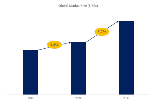
Según el nuevo informe de investigación de mercado “Informe del Mercado Global del Fuentes de luz de tritio 2024-2030”, publicado por QYResearch, se prevé que el tamaño del mercado mundial del Fuentes de luz de tritio alcance 0.03 mil millones de USD en 2030, con una tasa de crecimiento anual constante del 5.7% durante el período de previsión.
Figure 1. Tamaño del mercado de Fuentes de luz de tritio global (US$ Millión), 2019-2030
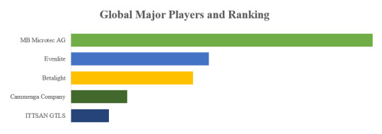
Según QYResearch, los principales fabricantes mundiales de Fuentes de luz de tritio incluyen MB Microtec AG, Evenlite, etc. En 2023, las tres principales entidades mundiales tenían una cuota de aproximadamente 70.0% en términos de ingresos.
Figure 2. Clasificación y cuota de mercado de las 5 principales entidades globales de Fuentes de luz de tritio (la clasificación se basa en los ingresos de 2023, actualizados continuamente)
Sobre QYResearch
QYResearch se fundó en California (EE.UU.) en 2007 y es una empresa líder mundial en consultoría e investigación de mercados. Con más de 17 años de experiencia y un equipo de investigación profesional en varias ciudades del mundo, QY Research se centra en la consultoría de gestión, los servicios de bases de datos y seminarios, la consultoría de OPI, la investigación de la cadena industrial y la investigación personalizada para ayudar a nuestros clientes a proporcionar un modelo de ingresos no lineal y hacer que tengan éxito. Gozamos de reconocimiento mundial por nuestra amplia cartera de servicios, nuestra buena ciudadanía corporativa y nuestro firme compromiso con la sostenibilidad. Hasta ahora, hemos colaborado con más de 60.000 clientes en los cinco continentes. Trabajemos estrechamente con usted y construyamos un futuro audaz y mejor.
QYResearch es una empresa de consultoría a gran escala de renombre mundial. La industria cubre varios segmentos de mercado de la cadena de la industria de alta tecnología, que abarca la cadena de la industria de semiconductores (equipos y piezas de semiconductores, materiales semiconductores, circuitos integrados, fundición, embalaje y pruebas, dispositivos discretos, sensores, dispositivos optoelectrónicos), cadena de la industria fotovoltaica (equipos, células, módulos, soportes de materiales auxiliares, inversores, terminales de centrales eléctricas), nueva cadena de la industria del automóvil de energía (baterías y materiales, piezas de automóviles, baterías, motores, control electrónico, semiconductores de automoción, etc.. ), cadena de la industria de la comunicación (equipos de sistemas de comunicación, equipos terminales, componentes electrónicos, front-end de RF, módulos ópticos, 4G/5G/6G, banda ancha, IoT, economía digital, IA), cadena de la industria de materiales avanzados (materiales metálicos, materiales poliméricos, materiales cerámicos, nanomateriales, etc.), cadena de la industria de fabricación de maquinaria (máquinas herramienta CNC, maquinaria de construcción, maquinaria eléctrica, automatización 3C, robots industriales, láser, control industrial, drones), alimentación, bebidas y productos farmacéuticos, equipos médicos, agricultura, etc.
0 notes
Text
Resistant starch technology supplier Microtec Engineering Group introduces FiberX™, a game-changing ingredient for healthier, fiber-enriched food production.
0 notes
Text
Equipo de unión de obleas, previsión del tamaño del mercado mundial, clasificación y cuota de mercado de las 13 principales empresas
Según el nuevo informe de investigación de mercado “Informe del Mercado Global del Equipo de unión de obleas 2024-2030”, publicado por QYResearch, se prevé que el tamaño del mercado mundial del Equipo de unión de obleas alcance 0.48 mil millones de USD en 2030, con una tasa de crecimiento anual constante del 7.5% durante el período de previsión.
Figure 1. Tamaño del mercado de Equipo de unión de obleas global (US$ Millión), 2019-2030
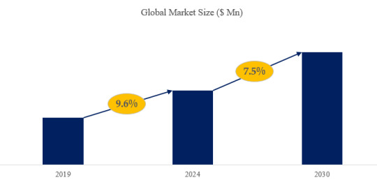
Figure 2. Clasificación y cuota de mercado de las 13 principales entidades globales de Equipo de unión de obleas (la clasificación se basa en los ingresos de 2022, actualizados continuamente)

Según QYResearch, los principales fabricantes mundiales de Equipo de unión de obleas incluyen EV Group, SUSS MicroTec, Tokyo Electron, Applied Microengineering, Nidec Machine Tool, Ayumi Industry, Aimechatec, U-Precision Tech, Shanghai Micro Electronics, Bondtech, etc. En 2022, las cinco principales entidades mundiales tenían una cuota de aproximadamente 84.0% en términos de ingresos.
Sobre QYResearch
QYResearch se fundó en California (EE.UU.) en 2007 y es una empresa líder mundial en consultoría e investigación de mercados. Con más de 17 años de experiencia y un equipo de investigación profesional en varias ciudades del mundo, QY Research se centra en la consultoría de gestión, los servicios de bases de datos y seminarios, la consultoría de OPI, la investigación de la cadena industrial y la investigación personalizada para ayudar a nuestros clientes a proporcionar un modelo de ingresos no lineal y hacer que tengan éxito. Gozamos de reconocimiento mundial por nuestra amplia cartera de servicios, nuestra buena ciudadanía corporativa y nuestro firme compromiso con la sostenibilidad. Hasta ahora, hemos colaborado con más de 60.000 clientes en los cinco continentes. Trabajemos estrechamente con usted y construyamos un futuro audaz y mejor.
QYResearch es una empresa de consultoría a gran escala de renombre mundial. La industria cubre varios segmentos de mercado de la cadena de la industria de alta tecnología, que abarca la cadena de la industria de semiconductores (equipos y piezas de semiconductores, materiales semiconductores, circuitos integrados, fundición, embalaje y pruebas, dispositivos discretos, sensores, dispositivos optoelectrónicos), cadena de la industria fotovoltaica (equipos, células, módulos, soportes de materiales auxiliares, inversores, terminales de centrales eléctricas), nueva cadena de la industria del automóvil de energía (baterías y materiales, piezas de automóviles, baterías, motores, control electrónico, semiconductores de automoción, etc.. ), cadena de la industria de la comunicación (equipos de sistemas de comunicación, equipos terminales, componentes electrónicos, front-end de RF, módulos ópticos, 4G/5G/6G, banda ancha, IoT, economía digital, IA), cadena de la industria de materiales avanzados (materiales metálicos, materiales poliméricos, materiales cerámicos, nanomateriales, etc.), cadena de la industria de fabricación de maquinaria (máquinas herramienta CNC, maquinaria de construcción, maquinaria eléctrica, automatización 3C, robots industriales, láser, control industrial, drones), alimentación, bebidas y productos farmacéuticos, equipos médicos, agricultura, etc.
0 notes
Photo

Lying on the floor [Yashica microtec zoom 70, Kodak Gold 200] @catchthirtysix
0 notes
Text
Surge in Demand for 3D Semiconductor Packaging Anticipated
In a significant development for the semiconductor industry, there is an imminent surge in demand projected for 3D semiconductor packaging. This surge is largely attributed to substantial investments in research and development by major industry players.

The demand for 3D packaged chips is expected to escalate sharply, driven by advancements in semiconductor technology and the need for more efficient and compact electronic devices. Key players in the semiconductor market are intensifying their efforts in R&D to capitalize on this trend and gain a competitive edge in the market.
𝐑𝐞𝐪𝐮𝐞𝐬𝐭 𝐏𝐃𝐅 𝐒𝐚𝐦𝐩𝐥𝐞 𝐂𝐨𝐩𝐲 𝐨𝐟 𝐑𝐞𝐩𝐨𝐫𝐭 (𝐈𝐧𝐜𝐥𝐮𝐝𝐢𝐧𝐠 𝐅𝐮𝐥𝐥 𝐓𝐎𝐂, 𝐋𝐢𝐬𝐭 𝐨𝐟 𝐓𝐚𝐛𝐥𝐞𝐬 & 𝐅𝐢𝐠𝐮𝐫𝐞𝐬, 𝐂𝐡𝐚𝐫𝐭)@ https://www.infinitivedataexpert.com/industry-report/3d-semiconductor-packaging-market#sample
Industry analysts suggest that the investments made by these leading companies are geared towards enhancing the performance, speed, and energy efficiency of semiconductor devices. This strategic focus underscores the growing importance of 3D semiconductor packaging in meeting the evolving demands of various technological applications.
The anticipated surge in demand for 3D packaged chips is not only poised to reshape the semiconductor landscape but also to accelerate innovation across industries reliant on advanced electronic components. As developments continue to unfold, stakeholders are closely monitoring these advancements to leverage the potential benefits offered by 3D semiconductor packaging.
𝐊𝐞𝐲 𝐂𝐨𝐦𝐩𝐚𝐧𝐢𝐞𝐬 𝐏𝐫𝐨𝐟𝐢𝐥𝐞𝐝 - STMicroelectronics , SUSS MicroTec , Amkor Technology, Inc. , IBM , Intel Corporation , QUALCOMM TECHNOLOGIES INTERNATIONAL, LTD. , Jiangsu SHEMAR Electric Co., Ltd. , Siliconware Precision Industries , TSMC , Micron Technology , 3M , AMD , Samsung Electronics , TOKYO ELECTRON LIMITED , Toshiba Corporation , United Microelectronics Corporation (UMC) , Xilinx
𝐑𝐞𝐪𝐮𝐞𝐬𝐭 𝐏𝐃𝐅 𝐒𝐚𝐦𝐩𝐥𝐞 𝐂𝐨𝐩𝐲 𝐨𝐟 𝐑𝐞𝐩𝐨𝐫𝐭 (𝐈𝐧𝐜𝐥𝐮𝐝𝐢𝐧𝐠 𝐅𝐮𝐥𝐥 𝐓𝐎𝐂, 𝐋𝐢𝐬𝐭 𝐨𝐟 𝐓𝐚𝐛𝐥𝐞𝐬 & 𝐅𝐢𝐠𝐮𝐫𝐞𝐬, 𝐂𝐡𝐚𝐫𝐭)@ https://www.infinitivedataexpert.com/industry-report/3d-semiconductor-packaging-market#sample
#3DSemiconductor#SemiconductorPackaging#AdvancedPackaging#ChipStacking#SystemInPackage#HeterogeneousIntegration#MultiChipModule#InterconnectTechnology#Microelectronics#FutureOfSemiconductors
0 notes
Text
Süss MicroTec: Attraktiver Wert in der Halbleiterbranche
Süss MicroTec: Attraktiver Wert in der Halbleiterbranche: https://www.it-boltwise.de/suess-microtec-attraktiver-wert-in-der-halbleiterbranche.html
0 notes
Text
as weird as it may sound, yesterday i went to mestre to have an interview with Microtec. yes the exact same company Filippo works in. in fact it was him who referred me to the company. i was running to the station in padova and then from the station in mestre to the company. fact: this time i liked mestre. more than padova. i like everywhere more than padova. sorry bro.
i'm sorry but life is weird?
It was exciting and also now that i realized I'm getting my period again for the second time in one month, i can tell how stressed i've probably been lately. I have got my defence session date. 8th of july. now it's 14th of june.
I don't wanna be too excited about yesterday cuz they told me it takes two weeks for them to give me a feedback on the interview. i usually don't rate things related to myself as positive, but i think i can vote that one as "no my worst work". it was my first technical and first job interview in presence. i was so socially inept the IT guy almost ran after me to shake hands with me after the interview ended cuz my stupidass was too stupid to remind to herself the social manners.
0 notes
Text
Nanoimprint Lithography System Market 2024 Size, Share and Growth by 2031

Global “Nanoimprint Lithography System Market” Report shows in depth analysis of global market size, share, regional and country-level analysis market segmentation, growth, share, competitive landscape, sales analysis. It is most comprehensive and important additions to industry that provides detailed research and analysis of key aspects of the global Nanoimprint Lithography System market. It provides information on the key growth drivers, constraints, challenges, trends and opportunities of market.
Get a Sample Copy of the Report at - https://www.proficientmarketinsights.com/enquiry/request-sample/1587
The global nanoimprint lithography system market size was USD 110 million in 2024 and the market is projected to touch USD 192.2 million by 2031, exhibiting a CAGR of 8.2% during the forecast period.
The Following Manufacturers Covered in the Nanoimprint Lithography System Market Report:
Obducat (Sweden)
Canon (Molecular Imprints) (U.S.)
Nanonex (U.S.)
SUSS MicroTec (Germany)
Market split by Type, can be divided into:
Hot Embossing (HE)
UV-based Nanoimprint Lithography (UV-NIL)
Micro Contact Printing (µ-CP)
Market split by Application, can be divided into:
Consumer Electronics
Optical Equipment
Others
Regional Analysis:
North America (United States, Canada and Mexico)
Europe (Germany, UK, France, Italy, Russia and Turkey etc.)
Asia-Pacific (China, Japan, Korea, India, Australia, Indonesia, Thailand, Philippines, Malaysia and Vietnam)
South America (Brazil etc.)
Middle East and Africa (Egypt and GCC Countries)
Inquire or Share Your Questions If Any Before the Purchasing This Report - https://www.proficientmarketinsights.com/enquiry/pre-order-enquiry/1587
The Study Objectives of Nanoimprint Lithography System Market are:
To analyze and research the global Nanoimprint Lithography System capacity, production, value, consumption, status and forecast;
To focus on the key Nanoimprint Lithography System manufacturers and study the capacity, production, value, market share and development plans in next few years.
To focuses on the global key manufacturers, to define, describe and analyze the market competition landscape, SWOT analysis.
To define, describe and forecast the market by type, application and region.
To analyze the global and key regions market potential and advantage, opportunity and challenge, restraints and risks.
To identify significant trends and factors driving or inhibiting the market growth.
To analyze the opportunities in the market for stakeholders by identifying the high growth segments.
To strategically analyze each submarket with respect to individual growth trend and their contribution to the market.
To analyze competitive developments such as expansions, agreements, new product launches, and acquisitions in the market.
To strategically profile the key players and comprehensively analyze their growth strategies.
Key Questions Covered in Nanoimprint Lithography System Market Report:
What will be the Nanoimprint Lithography System market growth rate and value in 2031?
What are the Nanoimprint Lithography System market trends during the forecast period?
Who are the Major players in the keyword Industry?
What is driving and Restraining this sector?
What are the conditions to market growth?
What are the opportunities in this industry and segment risks faced by the main vendors?
What are the forces and weaknesses of the main vendors?
Purchase this Report (Price 2900 USD for a Single-User License) - https://proficientmarketinsights.com/purchase/1587
0 notes
Text
0 notes