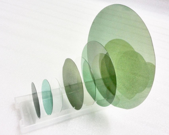
#sic wafer
Text
Global Top 7 Companies Accounted for 29% of total SiC Wafer Processing Industry Chain market (QYResearch, 2021)
SiC single crystal wafers have excellent heat resistance and voltage resistance compared to silicon wafers that are widely used for semiconductors. SiC single crystal wafers can remarkably reduce energy loss during electric power control, significantly contributing to the reduction of energy use and environmental stress. They are highly expected as substrate materials for the next-generation.
According to the new market research report “Global SiC Wafer Processing Industry Chain Market Report 2023-2029”, published by QYResearch, the global SiC Wafer Processing Industry Chain market size is projected to reach USD 1.33 billion by 2029, at a CAGR of 8.7% during the forecast period.
Figure. Global SiC Wafer Processing Industry Chain Market Size (US$ Million), 2018-2029

Figure. Global SiC Wafer Processing Industry Chain Top 7 Players Ranking and Market Share (Ranking is based on the revenue of 2022, continually updated)

The global key manufacturers of SiC Wafer Processing Industry Chain include Wolfspeed, II-VI Advanced Materials, TankeBlue, SiCrystal, Materials Research Furnaces, etc. In 2021, the global top four players had a share approximately 29.0% in terms of revenue.
About QYResearch
QYResearch founded in California, USA in 2007.It is a leading global market research and consulting company. With over 16 years’ experience and professional research team in various cities over the world QY Research focuses on management consulting, database and seminar services, IPO consulting, industry chain research and customized research to help our clients in providing non-linear revenue model and make them successful. We are globally recognized for our expansive portfolio of services, good corporate citizenship, and our strong commitment to sustainability. Up to now, we have cooperated with more than 60,000 clients across five continents. Let’s work closely with you and build a bold and better future.
QYResearch is a world-renowned large-scale consulting company. The industry covers various high-tech industry chain market segments, spanning the semiconductor industry chain (semiconductor equipment and parts, semiconductor materials, ICs, Foundry, packaging and testing, discrete devices, sensors, optoelectronic devices), photovoltaic industry chain (equipment, cells, modules, auxiliary material brackets, inverters, power station terminals), new energy automobile industry chain (batteries and materials, auto parts, batteries, motors, electronic control, automotive semiconductors, etc.), communication industry chain (communication system equipment, terminal equipment, electronic components, RF front-end, optical modules, 4G/5G/6G, broadband, IoT, digital economy, AI), advanced materials industry Chain (metal materials, polymer materials, ceramic materials, nano materials, etc.), machinery manufacturing industry chain (CNC machine tools, construction machinery, electrical machinery, 3C automation, industrial robots, lasers, industrial control, drones), food, beverages and pharmaceuticals, medical equipment, agriculture, etc.
0 notes
Text
Unveiling Growth Dynamics in the SiC Wafer Polishing Market

The SiC wafer polishing market is experiencing a surge, particularly driven by the expanding realm of greenhouse-protected cultivation. This article delves into the key drivers, restraints, opportunities, and challenges shaping the landscape, catering to chemical industry experts seeking a comprehensive understanding of this dynamic market.
Drivers: Increase in the Area for Greenhouse-Protected Cultivation One of the primary drivers propelling the SiC wafer polishing market is the notable increase in the area dedicated to greenhouse-protected cultivation. Chemical industry experts recognize the pivotal role SiC wafers play in optimizing greenhouse technologies, fostering an environment conducive to enhanced crop growth and yield. As the demand for greenhouse-protected cultivation rises, so does the demand for SiC wafer polishing, making it a crucial aspect for experts to monitor closely.
Restraints: High Cost of Installation Despite the evident advantages, the high initial cost of installing SiC wafer polishing systems poses a significant restraint. Chemical industry experts are well aware that the substantial investment required for the setup may deter some businesses from embracing this technology. Addressing this concern and exploring cost-effective solutions becomes imperative to encourage widespread adoption within the chemical industry.
Opportunities: Advancements in Technology The SiC wafer polishing market presents exciting opportunities with continuous advancements in technology. Chemical industry experts keen on staying at the forefront of innovation should monitor the evolving landscape of SiC wafer polishing techniques and technologies. From enhanced polishing methods to the development of more cost-efficient systems, staying informed about these technological advancements is key to unlocking new possibilities within the chemical industry.
Challenges: Lack of Awareness about the Benefits of Greenhouses A significant challenge hindering the widespread adoption of SiC wafer polishing technology is the lack of awareness about the benefits of greenhouse-protected cultivation. Chemical industry experts play a crucial role in disseminating knowledge about how SiC wafers contribute to creating optimal greenhouse environments, resulting in improved crop quality and yield. Overcoming this challenge requires collaborative efforts within the industry to educate stakeholders and drive awareness.
Download PDF Brochure :
Emerging Trends:
Smart Polishing Systems: The integration of smart technologies in SiC wafer polishing systems is gaining momentum. Chemical industry experts should keep an eye on trends involving the use of artificial intelligence and machine learning for precision polishing, resulting in improved efficiency and reduced wastage.
Environmentally Friendly Polishing Techniques: As sustainability becomes a focal point, new trends in SiC wafer polishing focus on environmentally friendly techniques. This includes the use of eco-friendly abrasives and polishing processes, aligning with the growing emphasis on green practices within the chemical industry.
Customization for Diverse Applications: The market is witnessing a trend towards customization to meet the specific needs of different applications. Chemical industry experts should explore how manufacturers are adapting their SiC wafer polishing systems to cater to the unique requirements of various chemical processes.
The SiC wafer polishing market offers a compelling landscape for chemical industry experts. By understanding the driving forces, addressing restraints, seizing opportunities through technological advancements, and tackling challenges related to awareness, experts can navigate this market successfully. As the industry continues to evolve, staying informed and proactive will be key to harnessing the full potential of SiC wafer polishing technology in the chemical sector.
0 notes
Text
[TIME is US Media]
U.S. and European officials are growing increasingly concerned about China’s accelerated push into the production of older-generation semiconductors and are debating new strategies to contain the country’s expansion.
President Joe Biden implemented broad controls over China’s ability to secure the kind of advanced chips that power artificial-intelligence models and military applications. But Beijing responded by pouring billions into factories for the so-called legacy chips that haven’t been banned. Such chips are still essential throughout the global economy, critical components for everything from smartphones and electric vehicles to military hardware.
That’s sparked fresh fears about China’s potential influence and triggered talks of further reining in the Asian nation, according to people familiar with the matter, who asked not to be identified because the deliberations are private. The U.S. is determined to prevent chips from becoming a point of leverage for China, the people said.
Commerce Secretary Gina Raimondo alluded to the problem during a panel discussion last week at the American Enterprise Institute. “The amount of money that China is pouring into subsidizing what will be an excess capacity of mature chips and legacy chips—that’s a problem that we need to be thinking about and working with our allies to get ahead of,” she said.[...]
Legacy chips are typically considered those made with 28-nm equipment or above, technology introduced more than a decade ago.
Senior E.U. and U.S. officials are concerned about Beijing’s drive to dominate this market for both economic and security reasons, the people said. They worry Chinese companies could dump their legacy chips on global markets in the future, driving foreign rivals out of business like in the solar industry, they said.[...]
domestic producers may be reluctant to invest in facilities that will have to compete with heavily subsidized Chinese plants. [...]
“The United States and its partners should be on guard to mitigate nonmarket behavior by China’s emerging semiconductor firms,”
While the U.S. rules introduced last October slowed down China’s development of advanced chipmaking capabilities, they left largely untouched [sic] the country’s ability to use techniques older than 14-nanometers. That has led Chinese firms to construct new plants faster than anywhere else in the world. They are forecast to build 26 fabs through 2026 that use 200-millimeter and 300-mm wafers, according to the trade group SEMI. That compares with 16 fabs for the Americas.
So what's the problem? is it that you suck at manufacturing & want more neoliberalism? That's what it seems like to me [31 Jul 23]
137 notes
·
View notes
Photo

Protons fix a long-standing issue in silicon carbide electronics
Silicon carbide (SiC) is a semiconductor material that outperforms pure silicon-based semiconductors in several applications. Used mostly in power inverters, motor drives, and battery chargers, SiC devices offer benefits such as a high power density and reduced power losses at high frequencies even at high voltages. Although these properties and its relatively low cost make SiC a promising contender in various sectors of the semiconductor market, its poor long-term reliability has been an insurmountable barrier for the past two decades.
One of the most pressing issues with 4H-SiC—a SiC type with superior physical properties—is bipolar degradation. This phenomenon is caused by the expansion of stacking faults in 4H-SiC crystals. Put simply, small dislocations in the crystal structure grow over time into large defects called "single Shockley stacking faults" that progressively degrade performance and cause the device to fail. Although some methods to mitigate this problem exist, they make the device fabrication process more expensive.
Fortunately, a team of researchers from Japan led by Associate Professor Masashi Kato from the Nagoya Institute of Technology, have now found a feasible solution for this issue. In their study published in the journal Scientific Reports, they present a fault suppression technique called "proton implantation" that can prevent bipolar degradation in 4H-SiC semiconductor wafers when applied prior to the device fabrication process.
Read more.
#Materials Science#Science#Silicon carbide#Electronics#Protons#Semiconductors#Defects#Stacking faults
17 notes
·
View notes
Text
System Shock (2023) - Impressions
My first serious game was Myst, and it demanded a very particular peripheral that used to be a mainstay of any serious gamer's arsenal: the double combo of a well-sharpened pencil and a generous Legal pad.
First came a story of Linking Books and filial betrayal. A little grisly in places, sure - thanks, Achenar - but mostly All-Ages stuff. I tore through two pads just to finish Myst because I had the insane idea of charting out the Selenetic Age's subway system organically. I was too dumb to realize the sounds were the same heard for the Mechanical Age's four cardinal points, too stubborn to bother, and armed with a summer's worth of game time and zero responsibilities. I charted out that damn subway for hours and screamed for joy when I lucked onto the exit.
Then came something a little harder on the nerves. A tale of corporate overreach, greed, megalomania pressed onto silicon wafers and a very Nineties vision of Cyberspace. Move over, Johnny Mnemonic, this hacker's even more hapless than you are...
Long story short, we open in a dystopian Cyberpunk future and are, in fact, a well-heeled chairjock. We've got the sick techwear to prove it, complete with glove-mounted ports for plugging portable data drives into your knuckles or socketing map-related proprioceptive enhancements to your wrist - like you do. The problem is, we've gotten a little long in the tooth and opted to steal a military enhancement that's probably omega cool, max nova or fraggin' awesome, depending on your other dystopian setting of choice. Said implant's owners and designers, the obscenely wealthy TriOptimum Corporation, sic their dogs on us. We're caught merely moments after stealing the schematics.
TriOp's Chairman of the Board, however, has some ideas. Ideas that work against the hardcoded ethical protocols of the AI system he both lords over and depends on, the Sentient Hyper-Optimized Data Access Network - or SHODAN. Space stations orbiting Saturn are complex hives of steel and flesh, you see, and designing a dispassionate and meticulous warden for it only made sense.
The problem is that thanks to your actions under duress, SHODAN is now anything but dispassionate and meticulous. She soon comes to see herself as a "living" goddess, and more or less rips a page out of AM-1's usual script. Kill the humans, experiment with their primitive flesh, turn their remains into obedient servants to her newfound magnificience - yadda yadda. On the plus side, SHODAN is once again voiced by Terri Brosius, former vocalist for the band Tribe - and she once again oozes cold and calculating menace. Glitchy cold and calculating menace, that is.
I mean - take five and go look at System Shock 2's now-famous opening CGI movie on YouTube. Look at you, hacker, said in its chilling tone of absolute contempt and utter surety of purpose, is now a bona fide classic Gamer Meme.
I might as well say that this is more or less The Game, as it were. as you spend most of your run trying to correct this very obvious SNAFU while also trying to figure out how you're going to leave a space station located halfway across the solar system when all the doors are locked and most relevant codes were either revoked or stashed away.
Oh, and the insane AI you're stuck with decided it was a good idea to start splicing tiger and gorilla DNA together into brand new cuddly murder machines. You know. For funsies.
Initially designed by Irrational Studios back in 1994 and now spruced up by Night Dive, this is a title that proudly foregoes several modern conveniences and that refuses to hold your hand even at the easiest difficulty settings you can configure. It isn't easily legible, its level design philisophy is intentionally outdated and if it could speak, it would spit in BioShock's direction and claim it was corrupted by the vainglorious promises of the Shooter Celebrity status.
And yes, I say that knowing BioShock is leagues removed from your average Call of Duty entry. Compared to System Shock, Bioshock is a Dudebro Machine designed to slam through brewskis while yelling about your KD ratio in a bad microphone. I'm also saying this as someone who loves Bioshock. System Shock the first in name is not friendly, it does not care for you or your concepts of builds or minmaxing, it almost sadistically throws a useless compass your way - and asks you to figure it out.
No handholding. No tutorials. No easing-into-things. Once you're on Citadel Station, you're on your own.
Honestly, just this is worth the price of admission. We've been coddled for decades, all because we're focused on making sure games recoup their massive budgets. System Shock sits at a lean and mean eight and a half gigabytes (yes! In 2023! It's shocking! Har har, easy puns!), it intentionally looks simple and chunky - and nothing is wasted here. Nothing whatsoever.
It's cramped, oppressive, dingy, menacing, cold, even possibly damp - and still a great showcase of any RTX-capable graphics card, with deep and believable shadows and so much Shader Porn that even the simple voxel textures that adorn the four sides of the playspace at all times feel properly anchored in the fiction. It's a beautiful game, if you're willing to understand that beauty as a concept can include pixels you can count with your naked peepers.
What it isn't, however, is forgiving towards younger gamers or anyone who skews towards more recent releases. The dual UI experience is instantly dated, the "inventory Tetris" concept stopped being fun long before Resident Evil 4 briefly revitalized it, and hitting Tab to click through audio logs and written notes for codes or clues when you can hear mutants wheezing and lumbering towards you is never really fun.
Y'can't pause, here - this is the Dark Souls of vintage PC horror games-
No, come on, that's a dated and cringey assertion, SHODAN's baby deserves better than that. What it is, though, is an encapsulation of a specific era in video game design and in what we once saw as constituting the best the Survival Horror genre could produce on our dated beige towers. The best outside of other classics in the genre, sure, but still one of the oft-cited references.
If you've got fifty or so bucks burning a hole in your pocket and the pressing need to have a skipping Text-to-Speech filter call you a pathetic insect, this is a must-have, quite simply.
6 notes
·
View notes
Text
Daily commenting on Dracula's shenanigans, I'll make this another two-parter because this story is getting dense, yo. 1/2:
Sometime during the evening, Jack is called to talk to Renfield who's very agitated. He takes the entire dude squad including van Hellstoker with him to the cell, and Renfield makes some surprisingly smooth conversation (including bootlicking Lord Godalming and the author's avatar, plus Stoker's eyebrow-raising speculations on the future of the United States) and asks to be released from the asylum immediately. Can only assume that his Master-Slave thingy with Dracula didn't go so well. Hey, not every dom is compatible with very sub. Jack, knowing Renfield's mood swings, doesn't want to rush, and when Renfield won't say why he needs to get the heck outta dodge right now, Jack is all: "Okay, bye!" Causing Renfield to beg frantically, and to warn Ominously(TM) that there's a lot of trouble coming their way. Jack nopes out of there with the dude squad.
Oh, great, Jonathan opens his journal entry by mentioning how strong and healthy Mina looks! *sigh* We all know what that means; Mina is a snack. And just to top it off, he literally says he's glad that she "hold[s] back and let[s] us men do the work". Twat. Pretty sure this particular sexism aspect will hold on for a while. When the dude squad notes some doubts if keeping Renfield in the asylum is the right thing to do, Jack points out that Renfield's connection to Dracula is a risky thing, especially when it comes to mind control. He calls Renfield "a respectable lunatic". I love Jack. Then the dude squad marches over to Dracula's estate where van Hellstoker gives another brief pep talk and hands out guns, knives, lamps (electric lamps, too; how fancy!), Communion wafers, crucifixes and garlic for everyone. As they enter, the fucking doors creak dramatically. Eh, I forget that this probably wasn't a cliché yet when the book was written. Van Hellstoker spits an incomplete Latin phrase into the dark, but their sneaking produces nothing but a lot of dust for now, although Jonathan feels like they are being watched.
Off to the chapel they go, which has some gross stench on it of earth and blood (Jonathan talks of "miasma"; when has everyone gotten thesausrus syndrome?). And only twenty-nine of fifty earth boxes. Also, the Count is watching them from the shadows, but these morons wave it all off as hallucinations because whoops, can't find anyone once we go there with lamplight! But so things won't get boring, Dracula sics the rats of the place on them. Arthur, bless his heretofore unknown brains, opens the next door and blows a dog whistle he brought along, calling a bunch of terriers to them. Pretty neat. Where did he get the doggos? And what does he mean by "lugubrious"? Can I hit Bram Stoker over the head with a dictionary? Arthur sends those good boys after the rats while the dude squad smokes a cigarrette or something similarly productive, and just ere break of day they calmly swagger home because this old spooky house is fascinatingly unfascinating after all. Van Hellstoker for some reason says this was perhaps their most dangerous step...? Counting boxes? Oh, it's Subtle Foreshadowing(TM); he's glad no harm or trouble has come to Mina in the meantime. Right.
Back at the asylum, they are greeted by a madhouse's sweet morning music - Renfield moaning, some other poor soul screaming; who cares. Jonathan finds Mina pale and with faint breath, and concludes it's good to keep her uninformed, since "it is too great a strain for a woman to hear". Brainless sexist asshole. Mina awakes not fully aware, with terror in her eyes, and complaining of still being tired; our Victorian himbo fails to catch on. Two things: Can Dracula use his boxes as teleportation localizations once they are placed elsewhere? Because that would be hella cool. And: Mina and Jonathan are newlyweds. Shouldn't he notice the bite marks sometime when he, you know, wants to take a more harmless nibble himself? Let's see how this goes.
#Dracula Daily#why does van Helsing the Foreigner(TM) know a bunch of fancy words no English person would use in everyday?#but can't get the basics of grammar and proverbs right?
7 notes
·
View notes
Text
0 notes
Text
Power Electronics Market - Forecast(2024–2030)
Switching electronic circuits are used to control the flow of energy in an electronic device. These switches are known as power electronics. Power electronics also helps in the conversion of power through semiconductor devices like diodes, transistors and thyristors. These devices can perform functions such as optimum forward and reverse backing capabilities. The devices are compact and can be used across a number of electronic devices across numerous applications. As of 2015, power electronics has become indispensable for applications related to renewable energy.

As a result of the numerous advancements in technology and R&D in the electronics sector, power electronics is being used across for almost all electronic devise, even more so for those in the industrial sector. The substrate technology used in power electronics plays a significant role in ensuring a more rugged device with a longer life-cycle. Power electronics provide high efficiency, and better electrical properties to withstand numerous life-cycles which is perfectly apt for applications such as aerospace, industrial and power.
Sample Report:
The power electronics market is being fuelled by advancements in the electronics industry and increase R&D spending in the same. As on date, the APAC region contributes the highest to the overall power electronics market with the Americas expected to post the highest growth during the forecast period. The APAC region is fuelled primarily by the number of industrial centers which are located in the region. Further to this, the region is home to almost 80% of all the electronics manufacturing which takes place globally and as such, power electronics are used by the OEMs directly in this region.
Inquiry Before Buying:
The market has been witnessing the onset of a large number of smaller players that are making headway into the market as well as a number of partnerships in terms of technology sharing and application penetration. In spite of the numerous advantages associated with power electronics, there are certain disadvantages which are inhibiting the growth of the market. The first being the high cost f production.
In terms of substrate wafer technology the market has been divided into the following GaN, SiC, and Others. The Power Electronics market has also been segmented by the following devices Power IC, Power Module & Power Discrete, diode rectifiers, ac-dc converters, ac-ac converters, dc-dc converters, dc-ac converters and static switches. The Power electronics market has also been segmented by the following applications Industrial, solar power, wind power, electric cars, aerospace and consumer electronics. The Power electronics market has also been segmented by the following geographies Americas, APAC, Europe and ROW.
Schedule a Call:
Following are just a few of the companies that are operating in the Power Electronics market:
Buy Now:
Fairchild Semiconductor
Hitachi Co
Infineon Technologies AG
Microsemi Corp.
Mitsubishi Electric Corp
For more Electronics related reports, please click here
1 note
·
View note
Text
[News] A 8-Inch SiC Wafer Fab Co-Built by San’an and ST to Start Production Soon | TrendForce Insights
0 notes
Text
All You Need to Know About Semiconductors in 2024

Semiconductors underpin nearly all facets of contemporary technology, from mobile devices and computing platforms to vehicles and automated home systems. Their role is increasingly critical as our world shifts more toward digital integration. In the past decade, the financial output of the global semiconductor industry has shown remarkable consistency, with revenues soaring past 520 billion U.S. dollars in 2023. This sustained growth illuminates the sector's crucial impact on the advancement of modern technology and its ability to swiftly adapt to market shifts. What catalysts are driving this industry growth, and what fresh developments might we see on the horizon? Let’s embark on a detailed exploration of the semiconductor landscape as it stands projected for 2024.

The Basics of Semiconductors
Occupying a middle ground between conductors and insulators, semiconductors are primarily composed of silicon, chosen for its reliable properties and natural prevalence. Their fundamental purpose is to manage electrical currents—this control is indispensable across all forms of electronic apparatus. Semiconductors' capacity to toggle between conductivity and resistance renders them essential for executing processing operations and managing data storage in myriad electronic formats.
Key Trends in the Semiconductor Industry
As we step into 2024, the semiconductor industry is witnessing swift transformations, spurred by the demands for more compact, potent, and energy-efficient chips. These enhancements are critical in accommodating emerging technologies such as artificial intelligence, the Internet of Things, and 5G connectivity. Such advancements not only escalate computing prowess but also advocate for superior energy conservation, underscoring the industry’s dedication to supporting the sophisticated needs of forthcoming technological applications.
Sustainability is now a core focus, prompting manufacturers to reduce energy use and waste in production processes. Amidst these shifts, following the semiconductor industry news is crucial, highlighting advancements like silicon carbide (SiC) and gallium nitride (GaN) semiconductors. These materials are celebrated for their efficiency and lower environmental impacts, aligning with the industry's push toward sustainability and performance. Collaborative efforts between companies and research institutions are also intensifying, accelerating innovation, and adapting to technological and societal needs.
Semiconductor Manufacturing's Technological Progression
The manufacturing processes in the semiconductor industry have been revolutionized by innovative developments this year. Among these is the wider implementation of Extreme Ultraviolet (EUV) lithography which has allowed for intricate and smaller chip designs through extremely fine circuit etching on silicon wafers, adding precision and pushing miniaturization to greater heights.
Architectural advancements such as 3D stacking that enables multiple layers of semiconductors stacked vertically without increasing footprint size, boost chip density alongside unparalleled efficiency features brought about by FinFET technology with its unique "fin" design shaping electrical current controls over transistors resulting in energy efficient chips with reduced leakage issues. This progress contributes significantly towards boosting computing power while improving environmental sustainability—a crucial aspect required for powering up future electronic devices.
Challenges the Semiconductor Industry Faces
The semiconductor industry, despite its significant growth and advancements, faces a range of serious challenges. A major issue is the scarcity of critical materials such as silicon and rare metals essential for chip production. These shortages are compounded by disruptions in supply chains that affect production capabilities and cause delivery delays. Additionally, trade disputes and regulatory issues on a geopolitical scale present considerable hurdles, impacting semiconductor companies worldwide.
These conflicts frequently result in higher costs and added complexity in operations. Furthermore, the industry must address technical hurdles as the physical limits of Moore's Law are approached. With transistor sizes nearing atomic scales, it becomes increasingly challenging to double chip performance every two years, driving the sector to explore new solutions and alternative technologies to maintain progress in semiconductor performance.
The Future of Semiconductors
Looking to the future, the semiconductor industry anticipates a trajectory of robust growth, highlighted by several promising advancements on the near horizon. Researchers are actively exploring innovative materials such as graphene, noted for its exceptional conductivity and versatility.
This material has the potential to redefine the architecture and efficiency of future electronic devices significantly. Simultaneously, the advent of quantum computing heralds a profound shift in computational dynamics. Quantum computers, which operate on the principles of quantum mechanics, are capable of tackling complex calculations that dwarf the capabilities of traditional computing systems, offering potential enhancements in semiconductor operations related to processing and data management.
These technological strides are not just pushing the envelope of existing capabilities; they are laying critical foundations for transformative developments that could redefine sectors from healthcare to cybersecurity, emphasizing the seminal role of semiconductors in the impending technological revolution.

Conclusion
Marked by swift innovation, significant obstacles, and vast potential, the semiconductor industry in 2024 continues to be a critical field. As reliance on technology intensifies across all facets of life, the importance of semiconductors is set to increase, positioning this area as a key one to monitor. Whether for enthusiasts, investors, or the merely curious about tech's future, keeping tabs on semiconductor developments is essential—they fundamentally underpin our digital infrastructure.
Read the full article
0 notes
Text
0 notes
Text
Exploring Nitride Bonded Silicon Carbide: The Super Material for Tough Jobs
Hello here! We are delving into the intriguing realm of Nitride Bonded Silicon Carbide, or NBSC for short today. Thanks to its remarkable qualities, this high-tech ceramic substance is creating waves in several sectors. NBSC could possibly be your new best buddy if you require something that can survive harsh environments. Let's investigate the reasons this substance is so unique, how it's created, where it's used, and why it's a game-changer.
Why Is NBSC so unique?
Mechanical strength
Let me start with strength first. NBSC is really robust. The nitride bonding technique lets it resist a lot of mechanical strain. This makes it ideal for times when things get tough and you want a substance that won't break or wear down readily.
Thermal Stability; Heat Not a hitch. Even at very high temperatures, NBSC performs really brilliantly. You will thus usually find it in locations like kilns and industrial furnaces. It also doesn't expand much when heated, so under thermal stress it is less prone to shatter.
Chemical Oppensity
When it comes to withstand chemical assaults, NBSC is like the materials' super hero. Whether it's molten metal, bases, or acids, this substance can manage it all without corroding. For use in chemical processing facilities and other demanding situations, that makes it perfect.
Resistance in Wear
NBSC is the choice if you require something that can keep on ticking and withstand abuse. It's quite robust and strong, which makes it ideal for mechanical seals and pump components—parts that will be heavily used.
The Making of NBSC:
Original Resources
High-purity silicon carbide (SiC) powder starts the path to produce NBSC. The base material is made from these mixed with silicon nitride (Si3N4).
Changing It Outline
NBSC can be shaped in numerous ways based on your demand. Often utilized are pressing, extrusion, and injection molding. The chosen method relies on the form, size, and complexity of the component.
The Nitide Bonding Mechanism
That's where the magic occurs. High temperature silicon carbide reacts with nitrogen to create silicon nitride. This technique guarantees everything bonds exactly by being conducted in a controlled surroundings. The outcome is a densified, extremely strong ceramic substance.
Smintering
The parts undergo sintering following the bonding procedure. Heating them slightly below their melting point causes the particles to combine into a solid form. Giving the material full strength and durability depends on this stage.
Where You'll Discover NBSC Industrial Kilns and Furnaces
Because NBSC can manage high temperatures and thermal shock, it is the go-to material for kilns and industrial furnaces. Often produced from NBSC are components including kiln furniture, burner nozzles, and furnace linings.
Wear- Resistance Parts
Where abrasion is a major concern, NBSC excels. Because it can resist a lot of wear and tear without degrading, it finds use in mechanical seals, abrasive blasting nozzles, and pump parts.
Chemical Processing Toolset
The resistance of NBSC against corrosion in chemical facilities is quite advantageous. Heat exchangers, reaction vessels, and pipe systems handling strong chemicals and high temperatures find application for it.
Metallurgical Uses:
In metallurgical operations, particularly with regard to molten metal handling, NBSC is also a mainstay. For parts like liners and crucibles, its chemical and heat tolerance makes it perfect.
Semiconductor Production
NBSC supports the manufacturing of high-purity silicon wafers in the semiconductor sector. Maintaining the purity and quality of these wafers depends critically on their chemical inertness and thermal stability.
Why NBSC is a game-changer in longevity and durability?
Long longevity of NBSC is one of its main advantages. Long-term savings of time and money result from its strength, wear resistance, and chemical inertness meaning components last longer and require less maintenance.
Performance Under Extreme Conditions
NBSC functions consistently regardless of extreme heat, corrosive chemicals, or abrasive surroundings. This makes it a flexible material with many possible demanding uses.
Economical Relevance
NBSC can be somewhat reasonably priced even with its sophisticated characteristics. Many businesses find it a wise decision as its great performance and low requirement for regular replacements and maintenance make it desirable.
Personalization
One can customize NBSC components to fit certain requirements. The manufacturing method can be changed to provide exactly what you require whether your needs call for a specific form, size, or feature.
In conclusion
Among materials with special combinations of strength, thermal stability, chemical resistance, and wear resistance is nitride bonded silicon carbide. From chemical processing tools to high-temperature furnaces, its adaptability and dependability make it priceless in many different fields. NBSC is expected to be a major participant driving innovation and efficiency forward as the demand for materials capable of handling ever challenging surroundings rises. Therefore, NBSC is most definitely worth looking at if you search for a substance that can withstand the heat (and much more).

0 notes
Text
Semiconductor manufacturer Nexperia to Invest 200 Million USD in Hamburg

Semiconductor manufacturer Nexperia today announced plans to invest USD 200 million (appx. 184 million Euros) to develop the next generation of wide bandgap semiconductors (WBG) such as silicon carbide (SiC) and gallium nitride (GaN), and to establish production infrastructure at the Hamburg site. At the same time, wafer fab capacity for silicon (Si) diodes and transistors will be increased. The investments are jointly announced with Hamburg’s Minister for Economic Affairs, Dr. Melanie Leonhard, on the occasion of the 100-year anniversary of the production site.
To meet the growing long-term demand for efficient power semiconductors, all three technologies (SiC, GaN, and Si) will be developed and produced in Germany starting in June 2024. This means Nexperia is supporting key technologies in the fields of electrification and digitalization. SiC and GaN semiconductors enable power-hungry applications, such as data centers, to operate with exceptional efficiency and are core building blocks for renewable energy applications and electromobility. These WBG technologies have great potential and are increasingly important for achieving decarbonization goals.
“This investment strengthens our position as a leading supplier of energy-efficient semiconductors and enables us to utilize available electrical energy more responsibly,” comments Achim Kempe, COO and managing director at Nexperia Germany. “In the future, our Hamburg fab will cover the complete range of WBG semiconductors while still being the largest factory for small signal diodes and transistors. We remain committed to our strategy of producing high-quality, cost-efficient semiconductors for standard applications and power-intensive applications, while addressing one of the greatest challenges of our generation: meeting the growing demand for energy and while reducing the environmental footprint."
First production lines for high-voltage GaN D-Mode transistors and SiC diodes started in June 2024. The next milestone will be modern and cost-efficient 200 mm production lines for SiC MOSFETs and GaN HEMTs. These will be established at the Hamburg factory over the next two years. At the same time, the investment will help to further automate the existing infrastructure at the Hamburg site and expand silicon production capacity by systematically converting to 200 mm wafers. Following the expansion of the clean room areas, new R&D laboratories are being built to continue to ensure a seamless transition from research to production in the future.
In addition to advancing technology, the semiconductor supplier expects the initiative to stimulate local economic development. The investments make an important contribution to securing and creating jobs and enhancing the European Union's semiconductor self-sufficiency. Nexperia works closely with universities and research institutes to benefit from each other’s expertise and promote highly qualified employee training. Nexperia relies on a robust research and development ecosystem in Hamburg and throughout Europe. Development partnerships and co-operations, e.g. in the field of GaN technology as part of the Industrial Affiliation Program (IIAP) of the nanoelectronics research center imec, play a crucial role. These and other collaborations ensure continuous innovation and technological excellence in Nexperia’s products.
"The planned investment enables us to bring WBG chip design and production to Hamburg. However, SiC and GaN are by no means new territory for Nexperia. GaN FETs have been part of our portfolio since 2019, and in 2023 we expanded our range of products to include SiC diodes and SiC MOSFETs, the latter in collaboration with Mitsubishi Electric. Nexperia is one of the few suppliers to offer a comprehensive range of semiconductor technologies, including Si, SiC, and GaN in both e-mode and d-mode. This means, we offer our customers a one-stop shop for all their semiconductor needs”, explains Stefan Tilger, CFO and managing director at Nexperia Germany.
The investment is yet another milestone in the 100-year history of Nexperia’s production site in Hamburg-Lokstedt. Since the foundation of Valvo Radioröhrenfabrik in 1924, the site has continuously developed and today supplies around a quarter of the global demand for small signal diodes and transistors. Since its spin-off from NXP in 2017, Nexperia has invested substantial sums in the Hamburg site, increased the workforce from 950 to around 1,600 and brought the technological infrastructure up to the state-of-the-art. This continued expenditure underlines the company's commitment to remaining at the forefront of the industry and providing innovative solutions to its customers worldwide.
Read the full article
0 notes
Text
0 notes
Last Seen Blogs

gaywrits
ICU

hesh3r
Hesh3r


georgiawinstonn
the past will eat you

rutobuka2
behold the fluff, actually