#vlsi physicaldesign
Explore tagged Tumblr posts
Visit Tumblr Blog
Explore Tumblr blogs with no restrictions, modern design and the best experience.
Last Seen Tumblr Blogs


Fun Fact
Users from the US are the majority of Tumblr visitors.
Photo

Get enrolled into one of those VLSI courses at SumedhaIT and let us help you shape your future and realize your dreams.
https://www.sumedhait.com/
https://www.sumedhait.com/physical-design/
https://www.sumedhait.com/custom-layout/
https://www.sumedhait.com/front-end-design-verification/
1 note
·
View note
Text
BEST VLSI Courses In Bangalore-Golden Light Solutions
We are a VLSI training institutes in Bangalore with 100% placement guaranteed VLSI courses in Bangalore Training with Industry Experts
0 notes
Text
What is Unateness in Static Timing Analysis?

Timing Sense corresponds to the functionality of the standard cells. It explains the traversal of a data from the source pin of the gate to its sink pin. Timing sense is also called as unateness of the timing arc.
All the standard cells can be classified based on the unateness they possess. Positive unate, Negative unate and Non-unate are the three types of unateness.
Under the timing section of a standard cell in .lib file, you can find timing sense information.
Positive unate: The rise transition at the source pin causes rise transition or no transition at the sink pin and fall transition at the source pin causes fall transition or no transition at the sink pin.
Standard Cells like AND Gate, OR gate, buffer possess this property.
Consider the truth table of AND Gate:
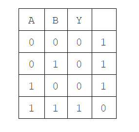
Consider the 1st case of inputs where both A and B are at logic 0 and output is at logic 0. Now consider B is getting transition to logic 1 then the output remains at logic 0 only (no transition). Now let A change to logic 1 then the output also transitions to logic 1.
Negative unate timing arc: The rise transition at the source pin causes fall transition or no transition at the sink pin and fall transition at the source pin causes rise transition or no transition at the sink pin.
Standard Cells like NAND Gate, NOR gate, inverter possess this property.
Consider the truth table of Inverter:
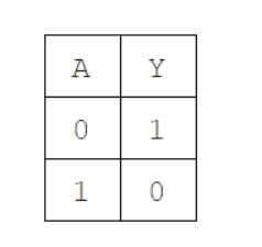
Signal transition on input A makes an opposite transition on the output pin Y.
Non unate: A standard cell which does not possess either of the property is said to be non-unate. XOR and XNOR gates have non-unate timing arcs.
Consider the truth table of XOR Gate :
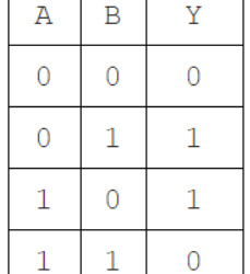
Consider the 1st case of inputs where both A and B are at logic 0 and output is at logic 0. Now consider B is getting transition to logic 1 then the output changes to logic 1. Consider the 3rd row, where output is at logic 1 with A at logic 1 and B at logic 0, now let B change to logic 1 then the output transitions to logic 0. The gate does not possess either of the property. Hence the timing sense of XOR gate is non-unate.
0 notes
Text
Physical design training institutes | Online physical design training institutes
5 Real Reasons Why Progressively More People Are Rushing Our Physical Design Training
In VLSI, physical design is transformation of net list to format in a given chip by meeting parts of region, power, execution (STA), and hence honoring time to showcase. Placement of cells, routing of metals that associate rationale entryways, floor plan, clock building, and meeting the required timing recurrence is the main objective of physical design.
It's among the chip design industry's most basic stages. It's the phase where most calendar delays are recouped to meet the TTM. Master liveliness, top to bottom examination and understating, faultless design, and demonstrated understanding, are the key necessities for getting a chip exactly on schedule and on the primary pass. These key necessities are definitely what we educate with our acclaimed physical design training. There are a few reasons why dynamically more individuals continue rushing to join the training and they include;
1. We Are a PhysicalDesign Training Institute With 100% Placement
As the preeminent of all physical design institutes in Bangalore, our understudies have confidence of 100% placement in the best item or administration based organizations in the wake of completing their physical design course with us. Likewise, we have the best of all physical design training institutes in Hyderabad which does likewise for our teeming understudies. Our 100% placement include has seen a portion of our past understudies building the most amazing vocations in the VLSI industry. That is the reason we are in front of all physical design training institutes in Hyderabad and around the globe.
2. Course Content
Our physical Design Training centers providing a full hands-around understanding of physical design training and physical verification training flow with complete laboratory work on using the most trending tools directly accessible in the industry. This is very not normal for other physical design training institutes in Bangalore or Hyderabad. Certainly, we've proceeded and none can find us.
After you complete this course, you will the flow of physical design from partitioning, power planning, clock tree union, physical verification, floor planning, timing examination, routing of practical unit squares, and close down checks. This likewise makes you a total ace of Physical Design. Things being what they are, which other physical design training institutes in Hyderabad offer substance that dives this deep? We give our understudies RTL to GDSii training so they can work between varying essential record positions.
3. The Best Physical Design Training Institute
Truly, we're certainly the best physical design training institute around but then we're a low cost physical design training institute. On the off chance that you contrast the little we accuse of the nature of our instructors, exercises, and materials, you will comprehend that we certainly offer parcels more an incentive for the cash our understudies pay. This by itself has guaranteed that we are seen by all industry specialists as a standout among st other physical design training institutes in India and around the entire world.
4. We are among the India's Top 10 Physical Design Institutes
Aside from being among the top 10 physical design institutes in India, we're additionally the no 1 physical design training institute in Bangalore. This shows the entire world is beginning to perceive our amazing commitments to the training and placement of the VLSI industry's future chiefs. We are among the top 10 physical design training institutes as a result of our really broad training program for top understudies in the electrical and hardware field.
5. The Course's Features
One of the key purposes behind this current course's continuously rising prominence is its key highlights. The significant ones are;
•
A hands-on introduction to the flow of physical design training with best tools that completely fulfill industry guidelines.
•
24/7 laboratory support with the conveyance of course materials and lab practice freebees by means of the best online physical design courses.
•
The advancement of delicate aptitudes with a total suite of physical design courses online which, are work arranged with 100% placement help after the consummation of the course.
•
Truly profound information on varying advances and systems utilized in physical design including DFT training.
•
Project execution that fulfills all industry guidelines from RTL to GDSii training, to hypothesis just as lab practice meetings that are under the direction of the industry's chief specialists who include over twelve years of VLSI teaching experience.
0 notes
Link
5 Real Reasons Why Progressively More People Are Rushing Our Physical Design Training
In VLSI, physical design is transformation of net list to format in a given chip by meeting parts of region, power, execution (STA), and hence honoring time to showcase. Placement of cells, routing of metals that associate rationale entryways, floor plan, clock building, and meeting the required timing recurrence is the main objective of physical design.
It's among the chip design industry's most basic stages. It's the phase where most calendar delays are recouped to meet the TTM. Master liveliness, top to bottom examination and understating, faultless design, and demonstrated understanding, are the key necessities for getting a chip exactly on schedule and on the primary pass. These key necessities are definitely what we educate with our acclaimed physicaldesign training. There are a few reasons why dynamically more individuals continue rushing to join the training and they include;
1. We Are a PhysicalDesign Training Institute With 100% Placement
As the preeminent of all physical design institutes in Bangalore, our understudies have confidence of 100% placement in the best item or administration based organizations in the wake of completing their physical design course with us. Likewise, we have the best of all physical design training institutes in Hyderabad which does likewise for our teeming understudies. Our 100% placement include has seen a portion of our past understudies building the most amazing vocations in the VLSI industry. That is the reason we are in front of all physical design training institutes in Hyderabad and around the globe.
2. Course Content
Our physical Design Training centers providing a full hands-around understanding of physical design training and physical verification training flow with complete laboratory work on using the most trending tools directly accessible in the industry. This is very not normal for other physicaldesign training institutes in Bangalore or Hyderabad. Certainly, we've proceeded and none can find us.
After you complete this course, you will the flow of physical design from partitioning, power planning, clock tree union, physical verification, floor planning, timing examination, routing of practical unit squares, and close down checks. This likewise makes you a total ace of Physical Design. Things being what they are, which other physical design training institutes in Hyderabad offer substance that dives this deep? We give our understudies RTL to GDSii training so they can work between varying essential record positions.
3. The Best Physical Design Training Institute
Truly, we're certainly the best physical design training institute around but then we're a low cost physical design training institute. On the off chance that you contrast the little we accuse of the nature of our instructors, exercises, and materials, you will comprehend that we certainly offer parcels more an incentive for the cash our understudies pay. This by itself has guaranteed that we are seen by all industry specialists as a standout amongst other physical design training institutes in India and around the entire world.
4. We are among the India's Top 10 Physical Design Institutes
Aside from being among the top 10 physical design institutes in India, we're additionally the no 1 physical design training institute in Bangalore. This shows the entire world is beginning to perceive our amazing commitments to the training and placement of the VLSI industry's future chiefs. We are among the top 10 physical design training institutesas a result of our really broad training program for top understudies in the electrical and hardware field.
5. The Course's Features
One of the key purposes behind this current course's continuously rising prominence is its key highlights. The significant ones are;
• A hands-on introduction to the flow of physicaldesign training with best tools that completely fulfill industry guidelines.
• 24/7 laboratory support with the conveyance of course materials and lab practice freebees by means of the best onlinephysical design courses.
• The advancement of delicate aptitudes with a total suite of physical design courses online which, are work arranged with 100% placement help after the consummation of the course.
• Truly profound information on varying advances and systems utilized in physical design including DFT training.
• Project execution that fulfills all industry guidelines from RTL to GDSii training, to hypothesis just as lab practice meetings that are under the direction of the industry's chief specialists who include over twelve years of VLSI teaching experience.
0 notes
Text

New Batch Announcement:
The enrollment process has already started. To enroll or inquire further, please contact on 9692807808 at any time or help us with your contact no so we can get in touch with you.
Venue: Rigel no 18 and 19 Aswath Nagar Marathahalli ORR Doddanakundi ,opp jeevika hospital (Karthik Nagar bus stop )
Bangalore, India"
Limited Seats Available.
PRE-BOOK YOUR SEATS NOW!!
👇👇👇
Commencement Date for Jan batch: 27th Jan 2020
For more detail: 📞 +91-9692807808
Register Now : http://bit.ly/2FIszh4
#vlsi #job #fresher#training #bengaluru#bangalore #sta #physicaldesign #STA #synthesis #analog #design #DFT #verification #IR #vlsi #job #fresher #training #bengaluru #bangalore#sta #physicaldesign#STA #synthesis#analog #design #DFT
0 notes