
Don't wanna be here? Send us removal request.
Statistics
We looked inside some of the posts by tessolve12 and here's what we found interesting.
Average Info
Notes Per Post
1
Likes Per Post
1
Reblog Per Post
0
Reply Per Post
0
Time Between Posts
13 days
Number of Posts By Type
Text
10
Last Seen Tumblr Blogs


Fun Fact
There were a total of 171.5 billion posts on Tumblr in 2019.
Text
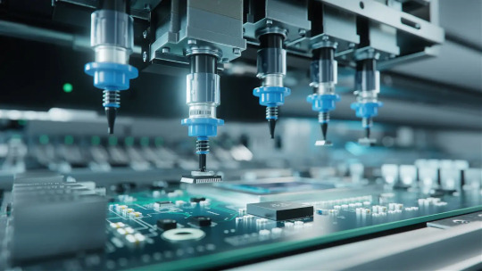
Cybersecurity In Embedded Systems: Securing The Smallest Attack Surfaces

Introduction
From pacemakers and household appliances to industrial control systems and driverless cars, embedded systems quietly operate at the core of vital processes in a world that is becoming more and more automated, intelligent, and connected. Their specialisation and small and sometimes disregarded existence in bigger systems are what make them so vital, but they also make them particularly susceptible. Because embedded systems are designed for specific functions, they present a concealed attack surface that is ready for exploitation, in contrast to traditional computing equipment. There has never been a more pressing need to safeguard these systems as they get increasingly intelligent and networked. The seven key ways cybersecurity is developing to safeguard the tiniest yet most important elements of the contemporary digital environment and embedded system design are listed below.
Cybersecurity in Embedded Systems: Securing the Smallest Attack Surfaces
Understanding that Safety Is Never Associated with Simpleness
The idea that embedded systems are secure because of their simplicity is a common misconception. Many of those devices are simply configured for a few operations, have little reminiscence, and do not have a whole working operating system. However, it is precisely this simplicity that draws attackers to them. Old vulnerabilities are a constant hazard since the majority of embedded devices operate on the same code for years without any changes. Frequently, its inflexible architecture leaves no space for intrusion detection or antivirus software. Attackers exploit this "set it and forget it" mentality by taking control of devices that were never supposed to be able to protect themselves by utilising well-known flaws. Building more robust, secure embedded systems begins with recognising this mistake.
Adopting Security-by-Design Guidelines Right Away
Security cannot be added after a system has been constructed. Since embedded systems have limited resources in terms of power, space, and computing capacity, it is imperative that cybersecurity be integrated from the bottom up. Strict authentication procedures, encrypted firmware, and secure boot procedures must all be included in the design blueprint by developers. Every part, from the communication module to the microcontroller, is assessed with cybersecurity in mind thanks to a secure-by-design methodology. Because embedded systems are increasingly handling real-time activities in national defence, healthcare, and transportation, it is not just good practice but also a must to design for security from the start.
Securing Channels of Communication in Environments with Limited Resources
Embedded systems are not isolated entities. Communication is continuous—and frequently unprotected—whether it's a smart thermostat sending a ping to a mobile app or a distant industrial sensor transmitting information to a cloud platform. A major obstacle, meanwhile, is putting robust encryption into devices with constrained computing capability. Elliptic Curve Cryptography (ECC) and TinySec are two examples of lightweight cryptographic algorithms that are currently being used to balance resource efficiency with security. Authentication layers are another component of secure communication that lowers the possibility of man-in-the-middle attacks by confirming the source and recipient. Making sure that even the tiniest communications are protected from prying eyes is the aim.
Firmware Updates Without Creating New Doors
Remotely updating embedded systems and advanced design solutions has changed everything; patches may now be used to close security flaws, add functionality, and correct issues. However, this power is reciprocal. Attackers may use a poorly secured update mechanism as a point of access. Embedded gadgets ought to confirm the integrity and authenticity of firmware previous to installation, which will prevent enhancements from introducing new vulnerabilities. Updates that are digitally signed and sent over encrypted channels are increasingly common. Additionally, putting rollback protection in place makes sure that malicious reinstallation of previous, possibly vulnerable versions is impossible. The goal of secure updates is to uphold confidence not only at launch but also during the device's lifespan.
Giving Unattended Device Physical Security First Priority
Embedded systems are frequently used in unprotected areas, including within consumer goods, automobiles, and factory floors. They are susceptible to manipulation because of this physical exposure. By getting direct access to the hardware, attackers can change firmware, obtain encryption keys, or intercept data. Physical incursion is being made more difficult by anti-tamper technology such as secure enclosures, epoxy encasements, and mesh sensors. Even if the primary device is hacked, more sophisticated methods like Trusted Execution Environments (TEEs) and Secure Elements (SEs) can safeguard private information. Physical security is equally as important as digital defence in a world where gadgets are left unattended yet are still supposed to remain safe.
Maintaining Supply Chain Stability in a Disjointed Environment
Chip makers, firmware developers, module suppliers, and integrators are some of the vendors that make up the embedded systems ecosystem, and all contribute to the finished product. Because of this fragmentation, the supply chain becomes complicated, and a single party's susceptibility might have an impact on the system as a whole. Verifying the integrity of hardware and code at every level, validating every component, and implementing safe handoff procedures are all necessary to ensure supply chain security. In high-risk businesses, tools like secure provenance monitoring and Software Bills of Materials (SBOMs) are becoming commonplace. The emphasis is now more on comprehending the origins of each component and how it was handled rather than merely creating safe systems.
Developing Resilience via Threat Detection and Monitoring
Historically, embedded systems were thought of as "set and forget" components that were only deployed once and hardly checked. That is rapidly changing. These days, even low-power devices are including anomaly monitoring and real-time threat detection. Smart warnings and actions are becoming crucial, whether the issue is anomalous network traffic, illegal access attempts, or changed memory behaviour. Even restrained systems can now analyse primary safety analytics locally to improvements in edge computing, identifying issues earlier than they turn out to be extra extreme. Long-term resilience is being able to swiftly detect, react, and recover from threats in addition to protecting against them. Passive embedded systems are outdated; they now need to actively defend themselves.
Conclusion
It is now a top priority to secure embedded systems and pcb design in usa as they are becoming more and more integral to our physical and digital infrastructure. These technologies' particular limitations necessitate equally particular security measures that combine creativity and accuracy. Every layer counts, from supply chain vigilance and real-time monitoring to safe design and communication protocols. The potential is as great as the challenge: we can safeguard the core basis of contemporary technology by considering embedded systems as first-class citizens in the cybersecurity discourse. It's time to turn every gate into a castle in a world where even the tiniest gadget may serve as an entryway.
0 notes
Text
How Test Engineering Ensures Quality In High-Volume Manufacturing
Test engineering is the vital link between production procedures and customer satisfaction in the intricate environment of contemporary manufacturing. Maintaining constant quality becomes considerably more challenging as manufacturing quantities rise to satisfy global demand. This field develops methodical techniques for finding flaws, confirming functioning, and guaranteeing dependability before items being delivered to customers by fusing technical know-how, statistical analysis, and process design. The Engineering Testing Services establishes the trust necessary for firms to increase production while upholding the quality standards that establish and safeguard brand name in cutthroat marketplaces, whether they are producing consumer electronics or automobile components.
Comprehensive Test Strategy Development
In high-volume production, careful test procedures that approach products holistically rather than as collections of discrete parts are the first step towards effective quality assurance. By examining possible failure modes, determining crucial performance metrics, and comprehending actual use situations that products would face after deployment, test engineers create these techniques. The resulting frameworks strike a balance between realistic limitations such as equipment investments, cycle time requirements, and production costs, and completeness. Functional verification, stress testing, environmental simulation, and statistical sampling are some of the testing approaches that are stacked correctly throughout the manufacturing process in well-designed strategies. By minimizing duplicate or low-value verification activities that would needlessly limit production throughput or raise costs without corresponding quality advantages, this strategic approach guarantees that testing resources focus on the most significant quality issues.
Automated Test Equipment Implementation
In high-volume manufacturing settings, automated test equipment that combines high-speed operation and precise measurement capabilities forms the foundation of quality assurance. These systems can be as basic as go/no-go verification stations or as sophisticated as integrated platforms that include environmental chambers, vision systems, and other test procedures. Successful implementations combine flexible software structures that allow for quick adaptation as products change with specially designed hardware interfaces tailored to the product. Advanced data collecting, statistical analysis, and closed-loop feedback to manufacturing equipment are all included in the automation, which goes beyond simple measurement. In contrast to traditional inspection methods that only detect issues after they arise, this integration establishes manufacturing ecosystems where test findings instantly drive process improvements before fault patterns can evolve, significantly lowering scrap rates.
Statistical Process Control Methodologies
The quality of high-volume production is largely dependent on statistical techniques that convert individual test results into useful process information. Instead of analyzing each product separately, statistical process control looks at measurement trends over time to differentiate between typical variation and notable changes that call for action. In order to determine when measurements show possible issues even when they fall within absolute specification limits, engineering test services develop quantitative frameworks and set control limits based on process capacity assessments. Multivariate analysis techniques are used in advanced implementations to find subtle interactions between parameters that would go undetected in conventional single-variable monitoring methods. By concentrating on process stability instead of trying to thoroughly check every aspect of the product, these statistical approaches allow producers to retain constant quality even as production quantities increase.
Design for Testability Integration
The best test engineers work closely with product development teams to integrate design for testability concepts even before production begins. This method acknowledges that the costs and efficacy of testing during mass manufacturing are directly impacted by product architecture. Test engineers collaborate with designers to include features that are expressly meant to make verification easier, such as modular architectures that enable independent subassembly verification, self-test routines that may rapidly check fundamental functionalities, and test points that give access to internal signals. These partnerships frequently entail trade-off evaluations that balance significant improvements in manufacturing quality against small design changes. When properly used, design for testability lowers capital equipment needs, increases fault coverage, and shortens test cycle times, resulting in significant competitive advantages through improved quality and lower manufacturing costs.
Failure Analysis and Corrective Action Systems
Test engineering involves more than just identifying faulty components; it also involves complex systems for determining the underlying reasons and putting long-term remedial measures in place. Instead of only treating symptoms, specialist engineering teams employ cutting-edge techniques like thermal imaging, chemical analysis, and scanning electron microscopy to carry out in-depth examinations into fault patterns found by test stations. These studies employ systematic approaches that take into account a number of possible variables, such as design robustness, environmental effects, process control, and component quality. The ensuing realizations propel methodical enhancements executed using official change management frameworks that confirm efficacy prior to complete implementation. Testing is transformed from a filtering function that only distinguishes between excellent and bad products into a continuous improvement engine that progressively improves overall production capabilities thanks to this methodical methodology.
Environmental Stress Screening Protocols
Environmental stress screening procedures are commonly included in high-volume production quality systems. These procedures expose items to controlled stress conditions, which hasten any breakdowns. These methods find latent flaws that would normally only become apparent after customers took ownership, in contrast to conventional functional testing that confirms present functioning. Common procedures include power cycling, vibration exposure, humidity change, and thermal cycling between temperature extremes; each is precisely calibrated to identify flaws without endangering devices that have been constructed correctly. By examining field failure data, calculating acceleration factors, and carrying out thorough reliability modeling, test engineers create these methods. When properly used, these screening techniques significantly boost long-term dependability by removing "infant mortality" failures, which may otherwise harm a brand's reputation and raise warranty expenses even when items pass common functional testing during production.
Measurement System Analysis and Calibration
Thorough measurement system analysis and calibration processes are necessary for ongoing assurance of the integrity of production test systems themselves. By measuring measurement variance, detecting possible bias, and confirming that test equipment can consistently differentiate between acceptable and unsatisfactory items, these activities guarantee that quality judgments are based on correct data. Gage repeatability and reproducibility studies, correlation analyses between several test stations, and routine verification using certified reference standards that may be traced back to national measurement institutes are examples of standard methods. Formal calibration intervals are set by test engineering teams in accordance with industry-specific regulations, stability studies, and criticality evaluations.
Conclusion
Through the establishment of methodical techniques to verification, analysis, and improvement, test engineering or vlsi chips serves as the vital cornerstone for quality in high-volume production. These methods change quality from a subjective objective to a quantifiable result by using well thought-out plans, automated execution, and ongoing improvement. Advanced test engineering becomes not only beneficial but also necessary for long-term manufacturing success as production volumes and product complexity rise.
0 notes
Text
Test Engineering For Ai And Edge Devices: Power, Performance, And Precision

The rise of AI and edge computing has caused major changes in the technology sector. With AI being used in edge devices, a new area of challenges has appeared in engineering. Today’s edge equipment such as robots, smartphones and devices used across industry, has to do demanding AI tasks using as little energy, keeping them cool and ensuring real-time performance as ideal as possible. The switch to intelligent edge devices means that quality engineering services must be highly capable to support their operations in many different environments and scenarios.
To test AI-enabled edge devices, specialists must understand hardware design, software validation, power improvement and AI algorithm checks. When companies focus on innovative products, strong product engineering services must address the issues in testing those products to ensure success. The article looks at the main aspects, rules and best practices in testing AI and edge applications, concentrating on saving power, achieving optimal performance and checking precision.
The Unique Testing Challenges of AI Edge Devices
Test methods for edge AI devices cannot be replaced with approaches used in earlier AI systems. In contrast to regular embedded systems, devices with AI at the edge use neural networks and machine learning and must function properly within the limited features of hardware. Most of the time, these devices call for particular quality engineering to verify how they function under different scenarios.
It is important to effectively test the AI software as well as the overall structure of the hardware it uses at the same time. Given how AI accelerators, memory and power management systems work together, proper testing methods should be used. PCB design service providers and test engineers ought to collaborate to make sure that the platforms are fully tested and easy to mass-produce.
Moreover, edge AI devices are often used in places where the connection is uncertain, power is unstable and the work they do can vary greatly. The role of test engineering includes testing devices for proper function under all the varieties of dynamic situations in which they may be used. For this reason, it is important to check how the software update functions, the security system and what happens during recovery when the device is at the network edges.
Power Efficiency Testing for AI Edge Devices
The amount of power consumed is very important for edge AI devices, especially in situations where energy is in short supply or devices rely on batteries. When testing these products, it is important to design power profiling methods that review energy consumption in different modes and while running varied programs.
Dynamic Power Profiling
Dynamic power profiling techniques are used by advanced quality engineering services to analyze how power is used during the inference process of AI. It requires performing high-resolution power measurements on different AI tasks being processed by the device so that engineers can locate excessive power use and find ways to improve performance. New test systems use precise instruments to monitor power in various domains, revealing the role that each part of the system plays in using power.
Thermal Management Validation
The better an edge AI device can manage heat, the more efficient it is with power. Product engineering services ought to verify that continuous usage of a device does not cause damage from overheating. Here, we must test the options available to dissipate heat, observe how the device cools itself down and see that the thermals never influence performance too much. The trend of making devices smaller and giving them more powerful processors makes it necessary to conduct thermal testing.
Battery Life Certification
Battery-powered AI edge devices have to be checked to ensure the battery can satisfy the set usage patterns. To do this, there should be automated tests that cover various situations and track power use, helping to estimate the battery life. By simulating a lot of usage in less time, specialized test frameworks allow the battery to be saved without harming key elements of AI in the system.
Performance Validation for Edge AI Systems
Edge AI systems should be tested to ensure their computational abilities and ability to respond instantly under all possible operating situations. The importance of performance means it’s essential to validate this when using effective quality engineering services.
Benchmarking AI Inference Speed
They rely on standard checks to determine how fast different AI models process different types of inputs. Such benchmarks should represent tasks that are usually found in the real world and deliver the same results whenever you run them. It is possible for advanced test automation frameworks to carry out hundreds of benchmarks and provide heatmaps showing where optimizations should be made and confirming the benefits of changes made after every project phase.
Latency and Responsiveness Testing
In edge AI applications, it is necessary that the work is performed quickly and predictably. It is important to measure latency from acquiring input all the way to taking some action by the robot. This calls for identical devices that measure the system’s reactions at high accuracy, with the difference down to a microsecond. Special test points and circuits designed into PCBs by experts can permit testing of the device without interrupting its regular operation.
Testing Edge AI Devices as a System
While testing components is helpful, the whole device should be tested as part of an entire system in actual usage settings. Using this method, all systems are able to function effectively in real-life situations.
Testing the entirety of the software
It is important for product engineering services to build thorough test cases that run the system from its sensors to its AI and outputs. During end-to-end testing, data travels through every section of the system and timing is ensured at each step of processing. Automated testing allows devs to regularly check their work and let them know, fast, when an error occurs.
Conclusion
As more AI becomes implemented in edge devices, engineers’ test methods should improve as well. Recent advancements in quality engineering involve solving the unique problems of ensuring how much power is used, the system’s overall performance and accuracy in modern technologies. If a company relies on wider product engineering services and advanced PCB design, it will have an edge over other companies in providing reliable AI edge devices that the market requires.
0 notes
Text
The Future Of Test Engineering In Chiplet And 3d Ic Architectures

Traditional monolithic designs are giving way to modular chiplet and 3D IC architectures in the semiconductor industry. This change opens the door to further integration and performance opportunities while addressing the escalating problems caused by Moore's Law. These sophisticated systems do, however, present special test engineering difficulties that traditional approaches are ill-equipped to handle. In order to guarantee reliability and performance in these next-generation semiconductor designs, test methodologies must change, as this article examines crucial Quality Engineering Services features for chiplet and 3D IC architectures.
Pre-Bond Testing: The Foundation of Reliable Integration
The crucial initial stage of quality control for chiplet designs is pre-bond testing. Each component needs to be thoroughly inspected to find any possible flaws before the separate chiplets are physically linked. By stopping defective parts from entering the integration process, this step avoids the expensive waste of perfectly good chiplets. In order to handle ever thinner silicon wafers, testing engineers must use specialized probe techniques that can reach smaller test pads. Effective pre-bond testing techniques must be implemented by striking a balance between thoroughness and pragmatism, as too much testing might increase expenses while too little testing could result in dependability problems with the finished product.
Die-to-Die Interface Testing: Ensuring Seamless Communication
Die-to-die interface testing is crucial because the communication channels between chiplets serve as the framework for multi-die systems. Across physical boundaries, these interfaces must consistently transport massive volumes of data at lightning-fast rates while preserving signal integrity. Verifying these interfaces presents special difficulties for test engineers, such as the necessity to replicate real-world operational circumstances and the scarcity of physical access points. Built-in self-test circuits are becoming more and more important, and new ways that combine structural and functional testing approaches are emerging. Test product engineering solutions must constantly modify their methods when die-to-die communication standards change in order to guarantee that these vital interfaces continue to function flawlessly under a variety of circumstances.
Through-Silicon Via Inspection: Navigating the Vertical Dimension
Reliability is crucial to system performance because Through-Silicon Vias (TSVs) act as the vertical highways that connect various layers in 3D IC layouts. These tiny holes drilled into silicon need meticulous production accuracy as well as equally stringent post-manufacturing inspection methods. To find tiny flaws like microvoids, fractures, or misalignments that can jeopardize electrical connection, test engineers use specialized equipment that uses ultrasonic, infrared, and X-ray technology. As TSV dimensions decrease and densities rise, the testing problem becomes more difficult and calls for increasingly advanced detection techniques. Engineers may now confirm TSV integrity during the production process without jeopardizing the structural integrity of these sensitive channels thanks to the ongoing development of innovative non-destructive testing techniques.
Thermal Management Verification: Controlling the Heat Factor
Since heat produced by lower layers is retained by upper layers, the stacked architecture of 3D integrated circuits poses previously unheard-of thermal problems that might result in performance loss or even irreversible damage. Advanced thermal testing techniques that can precisely detect and forecast the temperature distribution throughout the stack while it is operating must be developed by test engineers. Using infrared imaging methods, sophisticated thermal simulation models, and integrated thermal sensors are all part of this. Worst-case power consumption patterns are among the many operational situations that must be taken into consideration throughout the verification process. The validation of dynamic thermal management systems that can modify chip performance in real-time to maintain ideal operating temperatures throughout the whole integrated structure is becoming more and more important to test engineers as chiplet designs get more intricate.
Known-Good-Die Strategies: Maximizing Assembly Yield
The basis for producing chiplets in an economically feasible manner is the known-good-die (KGD) method. The idea is simple but difficult to put into practice: to optimize final assembly yield, thoroughly test and validate each individual die before integrating them. To obtain near-perfect defect detection rates without significantly increasing production costs, test engineers must create specialized wafer-level and die-level test procedures. This entails finding a careful balance between test economics and test coverage. This method is optimized by the use of adaptive test flows, in which test parameters change in response to trends in production data. KGD tactics continue to change as chiplet topologies become more varied, with a growing focus on standardized test procedures that preserve uniformity across different chiplet designs from different manufacturers.
Power Integrity Testing: Ensuring Stable Operation Under Load
The intricate problem of preserving a steady voltage and current distribution across multi-die systems under a range of operating loads is addressed by power integrity testing. There are many possible sites of failure because of the various power needs of distinct chiplets and the intricate power delivery systems required to sustain them. Even during periods of high processing demand, test engineers must confirm that power rails retain the proper voltages without making excessive noise or drooping. This calls for specialized testing apparatus that can concurrently monitor several power domains and replicate real-world power consumption patterns. Test procedures must change when chiplet designs include more complex power management features in order to confirm dynamic voltage and frequency scaling across die borders and guarantee that power-saving measures operate as intended without endangering system stability.
System-Level Testing: Verifying End-to-End Functionality
The final stage of verification is system-level testing, where engineers make sure the integrated chiplet assembly works as intended as a whole. All functional requirements, performance measurements, and reliability indicators of the finished product must be confirmed by this thorough testing process. The difficulty for test engineers is to create test plans that are both economical and comprehensive enough to handle the intricate relationships between many chiplets working together. This frequently calls for specialized test tools and advanced software that can put the system through a variety of operational situations. System-level testing is increasingly using artificial intelligence approaches to detect small performance irregularities and anticipate possible failure causes before they materialize in field circumstances as chiplet-based systems get more complicated.
Conclusion
An interesting intersection of innovation and difficulty exists in test engineering for chiplet and 3D IC pcb board design. Test procedures must keep developing as these cutting-edge designs become more widely used in order to guarantee dependability without causing delays in time to market. The rate of acceptance and eventual success of these ground-breaking semiconductor designs will be greatly impacted by the industry's capacity to work together to create efficient test solutions. The upcoming generation of high-performance computing systems will be made possible by more advanced, automated, and standardized test methodologies.
0 notes
Text
Digital Twin Technology in Test Engineering: Simulating Real-World Scenarios

Digital twin technology is transforming how companies test equipment, tools, and systems. In cities where precision and speed matter most, companies are using digital twins to carry out tests in a way that mimics reality. This saves teams time, reducing errors, and enabling them to make better decisions. Test engineering is one field where tremendous progress is being made. In this industry, several businesses are now dependent on smart tools like digital twins as part of digital transformation. Engineering Testing Services is one of the principal support systems in this area, which ensures this transition becomes smooth and streamlined.
Understanding Digital Twin Technology in Simple Terms: A digital twin is a virtual replica of something real. It might be a machine, a device, or even a whole system. The virtual replica is made with data and software. It acts just like the original, showing how it acts, moves, or reacts. If something happens to the real object, the digital twin is also affected. With this, one can learn how things will behave without working with the actual product. In engineering, digital twins enable testing to be safely and easily done. This comes in useful when manufacturing products like cars, machinery, or electronic parts. Engineers can use this twin to experiment if a machine will malfunction, overheat, or act weirdly.
Why Digital Twins Matter in Testing: Under normal testing, teams usually have to create a real model and test it repeatedly. This consumes time, resources, and real estate. Digital twins do away with all of these. With a virtual model, tests may be tested in several different environments without building anything. It also makes it possible for one to test dangerous ideas that are not safe to test in life. Engineers can now spot weak areas in advance. This avoids businesses having to make amends once the product is built. For engineering testing service-providing businesses, this technology offers a great deal of value. It helps in delivering faster, smarter, and cheaper results. With digital twins, tests can be conducted faster and repeated many times to be sure of the result.
Simulating Real-World Conditions: One of the strongest uses of digital twins in test engineering is the ability to simulate real-world conditions. Whether it's a car on a bumpy road or a piece of machinery under stress, digital twins can recreate the same event in software. This helps engineers understand how to behave their product. It also helps them predict unusual situations, like excess heat, rain, or pressure. These are very hard to achieve in the real world but easy to perform on a computer platform. The virtual model gives information, predictions, and suggestions to improve the product. This authority allows companies to avoid massive problems after they sell the product. This instills confidence in consumers and lowers returns and failures.
Assisting in Quick Prototyping: Constructing the initial form of any product, which is referred to as a prototype, can be costly. It usually requires revisions and redesigns. With digital twins, it is possible to create a virtual prototype and test it initially. This accelerates the design process. There is time to work out what does and doesn't work before any actual models can be created. Time from concept to functional product decreases by an enormous amount. Rapid changes are possible in the virtual environment. Components do not have to be manufactured and machines built. This also enables small businesses to test out extreme ideas without costing a fortune. In short, digital twins are making way for faster, smarter innovation.
Reducing Human Errors in Testing: In conventional testing, much depends on human effort. This can lead to errors, omissions, or faulty readings. Digital twin test systems reduce these errors. Since everything is software and data-driven, results are more accurate and replicable. Even if two teams run the same test, the digital twin will return the same result. This helps ensure high quality for every test. It also allows teams to see test results over time. Trends can be found and problems detected early. Human employees are still present, but the computer program does most of the work. This union of humans and software is making testing more accurate and trustworthy.
Improving Maintenance and Safety: Digital twins are not only useful during the stage of building and testing. They are also useful when the product is operational. For example, equipment can be monitored through their digital twins. If something goes wrong, the digital one can show what went wrong. This makes it simpler to fix issues. It also prevents issues from arising. If a part is deteriorating, the digital twin will show it. This is predictive maintenance. This is fixing something before it breaks. It also makes things safer. If a machine is broken, it can be stopped before it is dangerous. So, digital twins help to make machines safe and properly maintained in the long run.
Integration with Modern Technology: Digital twins also integrate easily with other modern technologies. They use sensors to collect data and artificial intelligence to process the data. This makes them intelligent and aware. They can learn from the last tests and offer improved directions the next time. They also fit perfectly into the tools that modern engineering teams use. These solutions include cloud platforms, remote controllers, and software for data analysis. Thus, irrespective of where the team members are located, they can have the same digital twin and test in parallel. This allows for collaboration and speeds up the process. As more tools become digital, digital twins will be even more useful. Their use in product engineering solutions will grow more in the future.
In conclusion, digital twin technology is turning out to be one of the most useful tools in engineering today. It allows teams to safely, rapidly, and accurately test products. It saves time, lowers costs, and improves quality. With the help of smart systems and data, it is helping teams get improved products to market. It is part of intelligent Engineering Test Services and helps businesses with each stage of product development. From conceptualization to finished product, digital twins are gaining prominence. And as this trend grows, so will the call for smart tools like digital twins. It is here too that areas like pcb board design will experience the most benefits, with testing and optimization being faster and more accurate.
0 notes
Text
TinyML: Bringing Machine Learning to Low-Power Embedded Systems

TinyML is changing the way technology is used by allowing machine learning to execute on very low-power and limited devices. This is quite helpful in the field of embedded system design where size, power, and memory are generally limited. Intelligent decisions can be made locally at devices such as microcontrollers and sensors with TinyML without having to transmit data to a big computer or the cloud. Not only does this save time, but it also enhances privacy and decreases energy consumption. With increasing businesses seeking intelligent and instant responses from their machinery, TinyML appears as a new mechanism to provide intelligence exactly at the point of need.
How TinyML Works: TinyML employs new tools and techniques to reduce the size of machine-learning models. The models are trained on large computers but are modified such that they can run on small chips. The models are trimmed down so that they will fit in devices with low memory, usually some kilobytes. TinyML also employs methods such as quantization and pruning, which reduce the model's size and accelerate its performance. Once the model is small enough, it can be incorporated into a tiny microcontroller that resides within a normal device, where it can begin making autonomous decisions.
Why TinyML is Important: One of the greatest advantages of TinyML is that it can add intelligence to the edge of a system. Rather than forwarding data from a device to a cloud server and then back again, all that occurs on the device itself. That is quicker and more secure. For instance, in an industry, a machine can detect and identify when there is something amiss and fix itself before failing. At home, a light bulb may learn your patterns and ignite automatically as required. A simple adjustment can result in significant energy and time efficiency, making the systems more efficient.
Real-World Applications: TinyML is now implemented in numerous locations. In agriculture, soil sensors employ it to know when the plants should be watered. In medicine, wearable sensors employ it to detect heartbeats and warn physicians of any hazard. Urban streetlights employ it to attain when to turn on, saving energy. Motors and machines in manufacturing employ it to detect any wear and tear, which saves money on repairs. These everyday applications demonstrate the extent to which TinyML can impact when properly utilized. It provides computers with the power of being smarter without needing massive computers.
Challenges of TinyML: Despite numerous advantages, there are a few challenges regarding TinyML. One of the largest issues is that the devices it executes take up very little space and use minimal power. It is challenging to deploy the complicated models and models with complexities because of this. It also takes expertise to confirm the models are fast and correct. Because the area of TinyML is new, the tools and experts are not available yet. Updating and testing the models may also be difficult because the devices will not always have internet access. Despite this, researchers and engineers are busy trying to address the challenges.
Tools and Frameworks: To assist developers in utilizing TinyML, some tools and software frameworks already exist. These tools assist in translating large models to small models and ease the ability to run on extremely small devices. Some of the tools specialize in reducing the size of the models, while others assist with testing and executing the models on certain chips. Some of these frameworks also support multiple microcontrollers, making them more flexible to design with. It is becoming easier for engineers to incorporate machine learning into everyday products because of these tools.
Data Privacy and Security: TinyML also assists in maintaining personal data security. Because the machine learning is occurring locally on the device, there is no need for sending sensitive information online. This makes the system secure and more personal. A good example can be a fitness tracker monitoring your health but not uploading your details to a cloud server. In production plants, personal data regarding operations is maintained inside the factory. This increases the level of security among users and gives trust to intelligent devices. One of the greatest reasons businesses are considering TinyML is data privacy.
Future of Intelligent Devices: The future of intelligent devices is being transformed using TinyML. With technology being smaller, things will be more able to think and make their own decisions. Smart devices in homes, cities, farms, and hospitals will all be included. It could mean that we have smart fridges that plan meals, smart roads that manage traffic, and smart clothes that monitor our health. They all become possible with the inclusion of machine learning into devices previously basic. The more popular TinyML becomes, the more places it will show up.
TinyML as a Smart Design Solution: TinyML is not only a tool but a smart design solution for modern challenges. It allows engineers to build systems that reason quickly and respond locally. With its appropriate usage, TinyML will make the product better designed and give manufacturers and consumers more value. Rather than having additional features, firms can build smarter features. It is soon becoming an important component of the process of developing the next set of intelligent, lightweight, and power-efficient products. Increasingly, industries today consider it to be an advanced design solution for getting ahead.
Education and Training: With TinyML being in increased demand, training on it also increases. Training schools and centers are now beginning to offer courses on how to design and deploy TinyML systems. Engineers and developers are learning new things to make smart systems with less power usage. Students even begin trying to deploy TinyML on small boards and kits. It assists in developing the field further and enabling anyone to participate more easily. Educating the masses is important to ensure that the new technology goes mainstream and is utilized correctly.
In conclusion, TinyML is quickly changing our perception of smart devices, especially in low-power and constrained space areas. With its ability to make devices smarter, faster, and safer, it is also efficiently driving industries. As engineers focus more on designing embedded systems and the market for smart, networked products keeps growing, TinyML is a new technology that stands out. In homes, hospitals, farms, and factories, the promise of TinyML is taking hold. With even greater innovation, TinyML will be a part of how we design new systems and products sooner than later, particularly in areas such as pcb design in usa where hardware and intelligence must function together in harmony.
0 notes
Text
The Rise Of Flexible And Foldable Pcbs In Consumer Electronics

The technological transition occurring inside electronic devices matches the fast pace of changing devices themselves in modern times. The evolution of consumer electronics receives transformative power through the development of flexible , foldable custom PCB board. Flexible circuit boards break traditional electronic design rules when they are produced for sleek modern electronics that become easily integrated into everyday use. Flexible PCBs serve as the core elements that allow smartphones to open and close while wearable fitness trackers match the human wrist shape.
1. The Evolution from Rigid to Flexible
Device designs were constrained to boxy shapes by the inflexible, flat nature of traditional PCBs. The requirement for electronics to fit into increasingly small and unusually shaped goods marked the beginning of the road toward flexibility. In order to allow circuits to bend without breaking connections, engineers created materials and manufacturing processes. It took years of development into conductive materials that could sustain repetitive flexing without losing their electrical integrity for this evolution to occur.
2. Space-Saving Advantages in Modern Devices
Electronic gadgets' use of space has been transformed by the capacity to fold and bend circuitry. Every millimeter matters in the cutthroat world of consumer electronics. Flexible PCBs can be curved to fit asymmetrical spaces that would otherwise go unused, folded into small configurations, or stacked in three dimensions. Manufacturers may either reduce the overall size of devices or fit more functions into the same footprint thanks to this space efficiency. Modern smartphones, for instance, can have more cameras, bigger batteries, and more features while still having thin profiles because flexible circuit designs save space.
3. Enabling New Form Factors and Designs
The rise of whole new device categories is arguably the most obvious effect of flexible PCBs. Without circuitry that can repeatedly bend at the hinge without degrading, foldable cell phones that open into tablet-sized screens would not be feasible. Circuit boards that can take on non-flat designs are also necessary for electronic fabrics, wraparound displays, and curved-screen televisions. Because the electronics may now adapt to the ideal product shape, product designers are no longer compelled to construct devices around inflexible rectangular boards. This paradigm change promotes industrial design innovation by enabling businesses to investigate organic shapes that are more conducive to human interaction.
4. Enhanced Durability and Reliability
Contrary to popular belief, flexible PCBs frequently perform better in durability testing than their rigid counterparts. When exposed to physical shock or vibration, traditional rigid boards might crack, leading to connection failures and irreversible damage. Flexible circuits, on the other hand, can withstand shocks by gradually deforming and then reverting to their initial state. They are perfect for portable gadgets that are subjected to drops or bumps on a regular basis because of their natural shock resistance. Furthermore, because flexible PCBs may be produced as a single continuous circuit, numerous solder joints that serve as failure spots in traditional designs are eliminated, resulting in fewer interconnection points overall.
5. The Role in Wearable Technology Growth
The wearable technology industry has expanded during the past years to make smartwatches and fitness trackers together with health monitors commonplace consumer items. The evolution of flexible printed circuit boards that could conform to human body contours would have limited the growth in this field. Devices used for prolonged wear require flexible features which rigid electronics technology cannot reproduce. The flexible nature of these circuits allows devices to match human body movements and maintain stable contact with the skin for accurate biometric monitoring and prevent any unwanted pressure on the skin. Flexible PCB technology enables wearable devices to stay discreet in daily life because their low weight reduces overall device mass.
6. Manufacturing Challenges and Innovations
Manufacturing processes experienced crucial developments due to the specific difficulties in producing flexible PCBs. Certain raw materials with particular manufacturing methods must be utilized to produce bendable conductive components. Manufacturers use modern printing technologies to establish new methods of tracing conductive tracks on flexible surfaces instead of using traditional etching methods. Traditional fiberglass boards resist heat damage better than flexible materials therefore maintaining proper assembly temperature remains essential. The production of flexible circuits has produced both specialized tools and procedures because of these technical obstacles. Flex PCB engineering technology that was previously reserved for high-end products because of manufacturing costs now reaches reasonable prices for consumer electronics through ongoing advancements and market scalability factors thus driving manufacturers to replace rigid circuitry.
7. Environmental and Sustainability Benefits
Compared to conventional rigid boards, flexible PCBs have a number of environmental benefits. Their decreased volume and weight result in less material being used, and their compact size frequently enables more effective shipping and smaller product packaging. Further lowering the amount of material needed, flexible circuits usually need fewer layers to accomplish the same functionality as multilayer rigid boards. The total amount of electronic waste produced is also reduced by doing away with large connectors. Compared to conventional rigid boards made of fiberglass, certain flexible PCB materials are also easier to recycle.
8. Future Prospects and Emerging Applications
The evolution of flexible and foldable PCB technology shows no signs of slowing. Current research focuses on stretchy electronics that can expand and contract while maintaining functionality, imagine devices that can be stretched to twice their size without damage. Other innovations include biodegradable flexible circuits for temporary electronic applications and self-healing conductors that can repair minor damages autonomously. These advancements will enable entirely new product categories, from rollable displays that unfurl from compact tubes to smart clothing with seamlessly integrated electronics. Medical applications are particularly promising, with flexible electronics enabling conformable sensors for continuous health monitoring and even implantable devices that match the contours of internal organs.
Conclusion
A significant change in the philosophy of electronic design may be seen in the emergence of flexible and foldable PCBs. With vlsi physical design manufacturers can produce gadgets that better meet human requirements through increased durability, greater ergonomics, and creative form factors by escaping the constraints of inflexible circuits. Flexible circuit technology will continue to grow in consumer electronics, opening up product categories we haven't yet thought of, despite ongoing difficulties with production scalability and cost reduction.
0 notes
Text
Test Engineering in Industry 4.0: The Shift Towards Smart Manufacturing

Manufacturing has been revolutionized by Industry 4.0, where digital innovations seamlessly unite with traditional processes, resulting in a world where automation, precision, and data-driven decision making prevail. In this article, we will see how test engineering has progressed to meet the modern production challenges, leveraging the emerging advanced testing methods, stringent quality assurance, and smart automation practices that are propelling production systems worldwide for reliable, efficient, and innovative manufacturing today.
Evolution of test engineering
The field of test engineering has transformed over the past decades as industries embraced digital innovations. Sophisticated techniques have replaced traditional methods to maintain efficiency and reliability. Adapting to increasing product complexity and dynamic market requirements has been driven by the evolution in test engineering and management. In manufacturing systems where sensors, data analytics, and automation are integrated, rigorous testing has become critical to operational success. This shift not only improves product quality but also optimizes processes by pinpointing problems early in the production cycle. Today, engineers use integrated software tools to monitor performance, simulate, and validate results in real time. The industry has been committed to innovation and quality control, resulting in the continuous improvement of testing protocols that have led to safer, more reliable products. With a focus on modern test engineering practices, they are a cornerstone in the transition to a data driven manufacturing ecosystem. The legacy they left behind continues to inspire future advancements across sectors worldwide.
Digital transformation in manufacturing
Manufacturing has been transformed by digital transformation, which has combined advanced computational methods and conventional industrial practices. Automation and real time data analytics have made operational workflows faster, smoother and error free. A robust engineering design testing process is essential to ensure that digital systems meet high quality and performance requirements. Engineers leverage digital twins alongside simulation models and cloud computing to forecast system behavior across different operational scenarios before starting production. The proactive nature of this approach shortens equipment downtime while enhancing total operational efficiency. Digital transformation allows companies to optimize resources, monitor system integrity continuously, and be able to adapt to market fluctuations at high speed. The convergence of digital technologies in manufacturing not only speeds up the process of innovation but also improves quality assurance protocols, making manufacturing processes more efficient and sustainable. If we want to achieve operational excellence and be successful over the long term in a competitive landscape, modern testing methodologies need to be integrated. It underscores the revolutionary impact of technology in manufacturing efficiency and product integrity.
Integration of automation systems
Modern manufacturing has achieved unprecedented efficiency and consistency through the implementation of automation systems. Modern manufacturing relies on automated processes to manage complex operations previously handled by humans which leads to faster production cycles and reduced errors. A thoughtfully designed PCB design board becomes crucial when multiple automation components need to communicate because it enables smooth data exchange between sensors, actuators and controllers. The combination of hardware and software creates real-time monitoring capabilities that enable adaptive control systems which sustain optimal performance levels. Automation technologies enhance both workflow optimization and data-driven decision support systems. Smart manufacturing development continues to rely on intelligent machinery integration with robust control systems to enhance operational efficiency. The integration of these elements establishes a fundamental base for developing flexible production environments that offer scalable capabilities and resilience to market changes. The PCB design board will remain central to future automation progress as new innovative approaches improve system interoperability and operational efficiency.
Advancements in quality assurance
Recent advances in quality assurance have changed the manufacturing landscape, emphasizing precision and reliability. Modern testing methodologies are strategically integrated to consistently meet rigorous industry standards. This framework of test engineering and management stands as a cornerstone to this evolution, balancing process control with technological innovation. Quality assurance protocols are constantly refined through the application of advanced analytics and machine learning to detect anomalies and mitigate risks. The result has been dramatic reductions in production defects and increased overall production efficiency. Automated inspection systems and predictive maintenance are now used in quality control to forecast potential failures before they occur, guaranteeing sustained performance. This makes manufacturers better positioned to provide superior products at less waste and greater resource utilization in a competitive marketplace. Additionally, continuous improvement practices promote process transparency and reliability, which in turn creates an environment where test engineering and management principles enable decision making and innovation. This systematic approach leads to production operations with enduring quality and sustainability.
Innovations in engineering design
Catalyzed by innovative approaches in engineering design, manufacturing methodologies have evolved into an era of precision and adaptability. The importance of the engineering design testing process has been emphasized on structured frameworks to evaluate each prototype thoroughly. This paradigm allows engineers to simulate real world conditions, assess structural integrity, and optimize design parameters before production. In this dynamic landscape, collaboration among multidisciplinary teams is essential to leverage insights from different areas to uplift the overall product performance. Design innovations are not only functional but also allow for increased cost efficiency and environmental sustainability. Advanced software tools and simulation platforms further strengthen the reliability of design outcomes in modern manufacturing facilities. Thus, companies are able to manufacture innovative and robust products that meet market demands and raise the bar for industry standards through continuous improvement and rigorous testing protocols. The engineering design testing process is further reinforced with continuous feedback loops and iterative refinements to provide reliability and optimum product performance.
Future prospects and challenges
The upcoming era of smart manufacturing shows promise but simultaneously presents multiple obstacles to overcome. Technology advancements transform production processes while driving new problem-solving methods. The growing complexity of modern systems demands better integration between digital tools and automation frameworks. The success of modern systems depends heavily on well-engineered PCB design boards that maintain both operational reliability and effective connectivity. The future of manufacturing will benefit from artificial intelligence alongside augmented reality and predictive analytics to drive advanced process optimization. However, issues such as cybersecurity, data integrity, and scalability present ongoing hurdles. The industry needs to overcome these obstacles while sustaining dedication to quality standards and innovation. Strategic partnerships combined with ongoing research will shape the next manufacturing era through adaptable production systems and resilient manufacturing environments. Research and development investments will continue to resolve emerging issues while strengthening the PCB design board's role in connecting technological advancements to dependable manufacturing processes.
The convergence of technology, rigorous testing, and innovative design defines smart manufacturing. Test engineering has evolved to change production with efficiency and quality. Digital solutions and robust automation are still being embraced by industry professionals. Continuous progress and focused improvements assure the future of manufacturing, securing reliability and excellence in the production process in every phase, worldwide today.
0 notes
Text
Test Engineering For 5g And Beyond: Ensuring Performance And Compliance

Introduction
Test engineering for 5G and beyond is a critical discipline that ensures that emerging communication systems meet stringent performance and compliance standards. Advanced methodologies are used by experts to validate network robustness, interoperability and security. Key testing approaches, integration strategies, and regulatory adherence to achieve effective performance in next generation wireless technologies are examined in this article. It specifies systematic practices for reliable operational excellence.
Evolving test methodologies for 5G networks
The acceleration in 5G technology necessitates new test methodologies to cope with increased complexity and varying use cases. In developing integrated frameworks to simulate real-world scenarios and capture critical performance metrics, engineers. Latency, throughput, error rates, and alignment with emerging standards are covered by comprehensive analysis. In this context, product engineering solutions are used to bridge the gap between design and operational requirements. The testing procedures include dynamic signal evaluation, protocol verification and environmental stress testing to enhance network resilience. It provides interoperability between different network elements and devices by providing systematic validation. These methodologies are based on detailed simulation and field trials and provide quantitative insights into system performance. Continuous improvement and rapid response to potential issues are enabled by rigorous analytical techniques and state-of-the-art instrumentation, which support efficient rollout of 5G infrastructure and beyond. These advanced methodologies not only improve reliability but also expedite time to market, creating robust communication networks that meet technical and regulatory requirements. They drive continuous innovation in network testing.
Integration of hardware and software systems
For accurate test engineering, the integration of hardware and software systems is critical. Modern test strategies focus on combining digital signal processing with physical layer hardware. In system architectures, engineers focus on modularity and scalability. The embedded system design is important as it ensures that hardware and firmware functions cohesively under diverse operational conditions. Diagnostic precision is enhanced by collaborative simulation tools and real-time monitoring techniques for fault isolation. The convergence of system components facilitates efficient troubleshooting and optimization. Circuit integrity, power distribution, and communication protocols are assessed using analytical methods. This approach gives you the ability to systematically test from the component level to end-to-end system performance. Iterative improvements, guided by detailed evaluations, lead to reliable systems that support high network demands and changing technological landscape. This rigorous integration process enables validation workflows to be streamlined, development cycles to be reduced, and complex infrastructures to achieve the high reliability and efficiency demanded by advanced wireless networks. Innovation drives continuous system improvement.
Performance verification and stress analysis
Ensuring that 5G networks work optimally, performance verification and stress analysis are key. Network behavior is tested under peak loads, variable signal strengths, and various environmental influences, using rigorous testing procedures. To confirm system reliability, metrics like data throughput, latency and error frequency are scrutinized. Component endurance is assessed using quality control engineering methodologies and circuit design weaknesses are identified. Empirical testing, supplemented by simulation, enables mapping of performance trends and prediction of failure modes. Stress tests are run systematically to validate design robustness under adverse conditions. Targeted diagnostics and advanced instrumentation are used by engineering teams to measure performance accurately. These tests provide insights that support iterative refinement to improve system performance and enhance service quality. Quantifiable benchmarks are provided via analytical models and statistical analyses, facilitating a structured approach to network optimization and long-term sustainability. Stress analysis is robust, system resilience is reinforced, and improvements in performance metrics and operational stability are guided.
Ensuring regulatory compliance and standards
Adherence to regulatory compliance and industry standards remains imperative in test engineering for 5G and future networks. System conformity to safety, security, and performance regulations is evaluated through structured testing protocols. Test results are detailed, documented and support transparency and verification processes for meeting mandatory certifications. Analytical models are employed to benchmark compliance levels and accommodate new requirements. Feedback from regulatory assessments is integrated into iterative testing phases to improve methodologies and overall system integrity. The testing process is rigorous, involving thorough audits and simulation of real-world operational scenarios to verify international standards. Evolution of network architectures is continually reviewed and validated against legislative frameworks and technical guidelines. They lower risks of non compliance and give users confidence in system performance. Central to achieving certification milestones across diverse regulatory environments are methodical evaluation and detailed reporting. Continuous improvement is driven by stringent compliance assessment that ensures networks operate within established regulatory boundaries, facilitating innovation and future growth.
Automation and data-driven test strategies
Automation and data-driven strategies change the test engineering game by improving efficiency and reducing human error. Real-time data acquisition and comprehensive performance tracking are enabled through advanced analytical tools. Structured validation processes can be easily integrated with test automation to rapidly identify anomalies. Statistical methods and machine learning algorithms are used by engineers to derive actionable insights from large amounts of data.These strategies help make the testing lifecycle more streamlined and support proactive maintenance. Iterative automation facilitates continuous adaptation to changing network demands and operational conditions. Decision-making and system functionality improvements are guided by meticulous data analysis that informs decision-making. This methodical approach decreases time to market and improves overall reliability. Automated test framework integration offers a scalable solution to complex architectures and varying network topologies, while maintaining consistent system performance in different conditions, and improving operational productivity and engineering innovation. Data-driven automation not only optimizes testing efficiency but also enables scalable growth and continuous improvement across comprehensive network deployments.
Future perspectives in test engineering
Future directions in the field of test engineering include adaptability to technological evolution and the complexity of network systems. Current approaches involve the use of artificial intelligence and predictive analytics to predict system failures before they even happen. Key to aligning testing strategies with rapid innovation cycles is advanced simulation techniques and iterative validation. The development of robust frameworks that accommodate evolving performance metrics and regulatory shifts is driven by research initiatives. Sustained improvements in network reliability result from continuous feedback loops and adaptive testing protocols. Next-generation testing standards are formulated through collaborative research efforts. Automated diagnostics and remote monitoring integrated progressively improve operational efficiency and facilitate scalable network expansion. A forward-looking approach positions test engineering as a critical enabler of technological progress in communication infrastructures, where performance and compliance remain key drivers for development. Next-generation networks are being formed by innovative research and strategic investments which continue to shape future testing paradigms, improving accuracy, efficiency, and reliability.
Conclusion
Test engineering for 5G and beyond continues to be a cornerstone for advancing next-generation communication systems. Testing is effective in optimizing performance, security, and compliance while accommodating the changing technological landscape. The systematic approaches presented herein provide clear frameworks for future innovations and operational excellence. Global connectivity and network reliability will continue to advance, driven by rigorous test engineering practices.
0 notes
Text
From Concept to Reality: How Mechanical Design Drives PCB Innovation
Today the US is the largest provider of printed circuit board design services and electronics manufacturing. Businesses and individuals alike may feel overloaded with options when looking for pcb design in USA. This post will help you identify the best partner for your electronic product development requirements and learn what distinguishes a PCB design service provider.
Knowing What Qualitative PCB Design Services Are
PCB design services are essential to launching cutting-edge goods in the quickly changing electronics sector. American design companies provide sophisticated design solutions by fusing decades of industry knowledge with state-of-the-art technology. These service providers have qualified engineers on staff who are knowledgeable about circuit board design theory and practice.
Essential Components of Excellent PCB Design Services
Several key competencies set the top PCB design services in the USA apart. They keep up-to-date design tools and software, guaranteeing accurate and effective design procedures. Their engineering teams provide clients with ideas that are both creative and feasible by staying abreast of the most recent manufacturing processes and industry standards.
These service providers usually provide thorough support from the beginning of the design process until the finished product. They know how crucial it is to maintain open communication with customers and give them daily updates on the status of their initiatives. This degree of involvement guarantees that the finished design satisfies all demands and criteria.
Advanced Design Capabilities and Solutions
Prominent PCB design companies in the US offer advanced design solution services to address challenging engineering problems. These companies excel in creating mixed-signal boards, analog circuitry, and high-speed digital designs. Their expertise extends to signal integrity analysis, impedance control, and managing complex layer stacks, ensuring reliable and efficient electronic designs for a variety of applications.
Modern PCB design requires sophisticated temperature management techniques and electromagnetic compatibility (EMC) considerations. Leading service providers reduce the need for expensive revisions by using sophisticated simulation tools to validate designs before manufacture. Additionally, they guarantee that designs adhere to industry norms and laws.
A Look at Manufacturing Considerations
The top PCB design services in the USA have a deep understanding of the manufacturing process. They produce designs that are both production-optimized and have good functionality. This entails taking into account elements like component positioning, assembly specifications, and testing accessibility. Their knowledge lowers production costs while preserving standards of quality.
These suppliers frequently keep up connections with different manufacturers, which enables them to suggest the best fabrication partners for particular projects. They make sure that designs are compatible with the intended production process by understanding various manufacturing capabilities and restrictions.
Documentation and Quality Assurance
An essential component of PCB design services is quality assurance. Prominent suppliers use stringent review procedures to identify possible problems early in the design stage. They keep thorough records of all design choices and specifications, which helps customers maintain and upgrade their products over time.
Knowledge and Proficiency
The most trustworthy PCB design companies in the US usually have a wealth of industry experience. They are able to contribute insightful opinions and best practices to every project because of their extensive exposure. They are able to offer tailored solutions for various applications since they comprehend the demands and difficulties unique to the business.
Customer Service and Interaction
Top PCB design companies stand out for their outstanding customer service. They give frequent updates on the status of the project and keep the lines of communication open throughout its duration. These companies recognize the value of efficiently managing project costs and meeting deadlines.
Innovation and Technology
Top PCB design services remain on the cutting edge of innovation. To improve their design skills, they keep spending money on new equipment and training. Customers benefit from improved product performance, dependability, and affordability thanks to their dedication to innovation.
Financial Aspects
The top PCB design services in the USA prioritize value over competitive pricing, even though cost is a significant consideration. They assist customers in realizing the long-term advantages of high-quality design work, such as lower production costs and increased product dependability. Usually, their pricing policies are open and honest, providing thorough justifications for every fee.
Excellence in Project Management
Effective project management is necessary for PCB design projects to be successful. Leading service providers manage projects from start to finish using organized procedures. They effectively manage resources, establish reasonable deadlines, and update clients on the progress of their projects and any obstacles that may arise.
Create for Upcoming Requirements
Future maintenance and upgrading requirements are taken into account by PCB design services while creating their designs. They design adaptable systems that can take into account future advancements or changes. Customers benefit from this strategy by saving time and money on subsequent product versions.
Accountability for the Environment
Environmental responsibility is also a top priority for PCB design services in the US. They adhere to environmental rules and use sustainable design techniques. This entails choosing parts and materials that preserve product functionality while adhering to environmental regulations.
Assistance for Research and Development
Research and development assistance is provided by numerous leading PCB design companies to assist customers in investigating novel technologies and advancements. They can aid with prototype design and proof-of-concept creation, which can help innovative ideas get to market more quickly.
Conclusion
To produce outstanding outcomes, the top PCB design services in the USA integrate technical know-how, cutting-edge design solutions, and first-rate client support. Take into account a service provider's expertise, skills, and dedication to excellence before choosing one. Seek out suppliers who can show a history of completed projects successfully and who are aware of your unique requirements.
In addition to designing circuit boards, the ideal PCB design partner will help your product succeed by offering creative solutions and dependable assistance. In order to ensure that designs are optimal for manufacturing and long-term durability, they will assist in navigating technical hurdles. Given how quickly technology is developing, picking a supplier who keeps up with market trends and upholds high standards of quality is essential for success in the cutthroat market of today.
Recall that effective PCB design involves a thorough comprehension of the complete product development process and extends beyond technical standards. This comprehensive bundle is provided by the top US providers, who assist customers reach their objectives while upholding strict quality and dependability criteria. You may invest in the future success of your product and lay the groundwork for future innovation and expansion by selecting the best PCB design service provider.
1 note
·
View note