#PCB Layout Experts
Explore tagged Tumblr posts
Visit Tumblr Blog
Explore Tumblr blogs with no restrictions, modern design and the best experience.
Last Seen Tumblr Blogs


Fun Fact
The Tumblr office adopted Tommy, an 11-year-old Pomeranian.
Text
PCB Designing Company in Gujarat
Innovative PCB solutions in Gujarat! Leading design company, expert in precision layouts for optimal performance. Elevate your electronics with us.Get more info and contact details in India.
#PCB Designing Company#Printed Circuit Board Design Services#PCB Layout Experts#Electronic Design and Manufacturing#Custom PCB Design Solutions#High-Quality PCB Prototyping#Gujarat PCB Fabrication
0 notes
Text
AC PCB Repairing Training Institute
AC PCB Repairing Training Institute: Skill Development
With the increasing demand for ventilation in homes, offices, and workplaces, maintenance planning and maintenance are essential.AC PCB Repairing Training Institute The most important part of an AC system is the circuit board or PCB, which controls the operation of the AC system. Teaching is a great profession where you have to study and get good grades. That’s where the AC PCB Knee Repair Academy comes into play.

Why choose AC PCB Repairing Training Institute?
Enrollment in a professional training school offers the person structured, practical training that cannot be obtained by self-study.AC PCB Repairing Training Institute Professional training teaches students technical skills in AC PCB systems, provides them with practical sessions, and prepares them for actual repair situations. Training schools also give students up-to-date information on the latest trends and tools utilized in the trade.
Major Benefits of Training
An efficiently structured training course covering theoretical and practical topics of PCB repairing.
Practical training in equipment and techniques used in the electronics repairing business
Practice exposure in actual AC PCB faults under the guidance of experienced trainers.
Certification to improve trainees' credibility and marketability.
Training in safety procedures, customer service, and service reporting.
Course Content and Learning Outcomes
A successful AC PCB Repairing Course includes the following:
Introduction to AC components and their uses
PCB design and layout concepts
Understanding the working principle of air conditioners
Decision and diagnosis of common faults in AC PCB
Soldering and desoldering techniques
Use of measurement devices such as multimeters and oscilloscopes
Step by step process of repairing and replacing faulty components
Precautions while repairing
Upon successful completion of this course, students can repair and diagnose various types of AC PCB-related faults independently.
Who should take the course?
This course is suitable for all types of individuals, such as:
School passouts or ITI students interested in technical and job-fit skills
Technicians and electricians who want to offer extension services
Those interested to start small AC or electronics repair shop businesses
Hobbyists interested in repairing circuits and electronics
The course is able to handle fresh entrants with no technical background as well as experienced candidates with experience in electronics.
Choosing the Right Training Institute
While choosing an AC PCB Repairing Training Institute, the following should be kept in mind:
A well-designed syllabus with theory and practical training
Trained faculty with hands-on industry experience
Availability of recent tools and test equipment for training
Good ratings and feedback by students
Employer- and service center-approved certification
Job placement facilities or internship exposure
Choosing a local institute can also provide greater convenience and accessibility.
Career Opportunities After Course Completion
Completing a professional course in AC PCB Repairing makes one conscious of numerous job opportunities, such as:
AC repair specialist with specialized PCB services
Brand service center air conditioner engineer
Independent PCB repair specialist
Home AC repairing and maintaining business owner
Technical support experts in appliance companies
After experience and training, a person can be a good professional in a growing field.
Last Words
Professional training facility AC PCB Repairing Training Institute is a smart investment for any individual who desires to start an electronics repair business. It not only provides real, job-oriented skills but also introduces opportunities for self-employment and professional growth. Choosing an appropriate training facility ensures that you are getting quality training, proper certification, and guidance to be successful in the business.
Begin your career path today by joining a reliable AC PCB Repairing Training Institute and become proficient and confident enough to be a professional electronics repair technician.
2 notes
·
View notes
Text
Mastering Circuit Board Design: The Backbone of Modern Electronics
In the ever-evolving world of electronics, Circuit Board Design plays a critical role in shaping the functionality and performance of devices we rely on daily—from smartphones and laptops to IoT devices and automotive systems. As the demand for compact, efficient, and high-performance electronics grows, so does the importance of well-executed circuit board design.
🧠 What is Circuit Board Design?
Circuit Board Design, also known as PCB (Printed Circuit Board) design, is the process of creating the layout of electrical circuits that connect components such as resistors, capacitors, and microchips on a non-conductive board. The objective is to ensure optimal performance, durability, and manufacturability of the electronic device.
🔍 Key Steps in Circuit Board Design
Schematic Capture The first step is designing a schematic—a symbolic representation of the electronic circuit. This blueprint outlines how each component connects and interacts.
Component Placement Components are placed on the board considering signal integrity, heat management, and physical constraints.
Routing the Traces Routing connects the components using copper traces. This step demands precision to avoid interference and ensure electrical performance.
Design Rule Checks (DRC) Tools are used to verify that the design meets specific electrical and manufacturing requirements.
Prototyping & Testing Before mass production, a prototype is developed and tested to identify and resolve any functional issues.
⚙️ Tools Used in PCB Design
Some popular tools that aid in circuit board design include:
Altium Designer
EAGLE
KiCad
OrCAD
Proteus
These tools allow engineers to simulate, design, and test circuit boards efficiently.
🚀 Emerging Trends in Circuit Board Design
High-Density Interconnect (HDI) PCBs for compact designs
Flexible and Rigid-Flex PCBs for wearable tech and medical devices
AI-Driven PCB Design Tools for faster and error-free layouts
Thermal Management Innovations for heat-sensitive components
💡 Why Circuit Board Design Matters
A well-designed PCB:
Enhances device reliability and longevity
Reduces signal interference and noise
Simplifies manufacturing and testing
Supports compact, lightweight, and modern designs
Whether you’re a hobbyist or a professional engineer, mastering PCB design is essential for developing innovative and efficient electronics.
��� Final Thoughts
Circuit board design isn’t just a technical requirement—it’s an art form that blends logic, creativity, and precision. The demand for expert PCB designers will only grow as industries lean more into automation, AI, and miniaturized electronics.
If you’re diving into the electronics space, learning the ins and outs of circuit board design can open doors to exciting opportunities in tech.
1 note
·
View note
Text
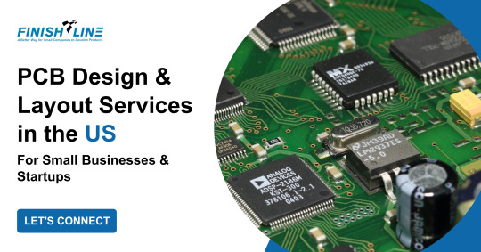
FinishLinePDS is a US based Product Development firm. We go beyond layout by complementing your team with experts, process, and reference designs that improve quality and decrease cost.
First, we do a complete review of the schematic and BOM. Independent reviews have been shown to decrease the number of “spins” substantially. This reduction in spins not only saves cost but decreases time to market.
For more information, visit: PCB Design and Layout Services
#PCB#PCBLayout#PCBDesign#ProductDevelopment#ProductDesign#EngineeringHelp#TechnologySolutions#Startups#BusinessStartups#TechStartups#SmallBusiness#SmallBusinesses#SmallBusinesstips#Startup#ProductDesigns#Innovation#InnovationDesign#Innovations#Entrepreneur#Entrepreneurs#Entrepreneurship#FinishLinePDS
2 notes
·
View notes
Text
Thermal Simulation Tools Are Evolving—Is Your Workflow Keeping Up?
Simulation Is No Longer Optional
Designing electronics without thermal simulation today is like racing without a dashboard, you might keep moving, but you’ll miss the warning signs. With tighter enclosures, higher power densities, and diverse operating environments, thermal challenges aren’t just probable—they’re inevitable.
Modern Mechanical & Thermal Design workflows are evolving fast. Simulation tools have become more intelligent, more accessible, and more essential. The real question is: has your workflow kept up with the change?
Why Thermal Simulation Is Getting Smarter
A few years ago, thermal simulations were mostly post-layout activities. Now, they’re integrated earlier in the design phase, sometimes even during concept development.
What’s driving the change:
Compact form factors with high power loads
Multi-board systems generating localized heat
Demands for silent (fanless) cooling
More design teams working remotely and asynchronously
These pressures make it critical to simulate heat flow, temperature gradients, and component interactions early in the process. That’s where Mechanical & Thermal Design takes center stage.
What Modern Tools Bring to the Table
Today’s simulation platforms aren’t just about running heat maps. They’re smarter, faster, and often integrated with your PCB and CAD tools.
Here’s what’s new:
Intuitive interfaces for 3D airflow modeling
Real-time co-simulation with mechanical CAD
Faster meshing algorithms that don’t need expert tweaking
Cloud-based options for collaborative work
With these features, Mechanical & Thermal Design is no longer siloed—it becomes a fluid part of the product design journey.
The Cost of Outdated Workflows
Still relying on spreadsheets, ballpark guesses, or legacy simulation methods? You’re likely leaving performance and time on the table.
Outdated approaches can lead to:
Over-engineered cooling systems (cost and space waste)
Missed hot spots that cause long-term failures
Design delays due to thermal issues in late-stage testing
Modern Mechanical & Thermal Design practices use simulation not just to fix problems but to prevent them from happening in the first place.
Early Simulation = Fewer Surprises
Integrating thermal simulation during early mechanical concepting avoids cascading design changes later. Whether you're using passive cooling, forced airflow, or heat sinks, the earlier you simulate, the better your decisions.
Benefits of early-stage thermal simulation:
Faster time-to-market
Smaller, more efficient enclosures
Fewer physical prototypes
Tighter collaboration between electrical and mechanical teams
Thermal modeling is now a strategic step in the Mechanical & Thermal Design process—not just a safety check.
Real-World Integration Tips
If your team is moving toward integrated simulation, here are a few quick tips:
Model real-world conditions: Include surrounding components, airflow paths, and mounting orientations.
Use 3D board models: Import IDF/STEP files to ensure geometry is accurate.
Validate against extremes: Simulate worst-case power and ambient temperature scenarios.
Involve mechanical engineers early: They understand enclosure constraints that affect cooling.
These strategies help you get the most from your Mechanical & Thermal Design simulations.
Why It Matters More Than Ever
Products are getting smaller, hotter, and expected to last longer. Your mechanical and thermal considerations need to evolve just as fast.
It’s no longer about just surviving temperature—it’s about:
Meeting performance targets
Achieving compliance
Extending product lifespan
Delivering consistency in every unit shipped
All of which are tied to one core capability: how strong your Mechanical & Thermal Design workflow really is.
Final Thoughts
Thermal simulation tools are not only evolving, they’re becoming essential allies in creating better products. If you’re still waiting until the end of a project to think about cooling, you're already behind.
It’s time to treat Mechanical & Thermal Design not as a checklist item, but as a dynamic, simulation-driven pillar of your product development process.
FAQs
Q1: Do I need thermal simulation if my design isn’t high-power?A: Yes. Even low-power devices in enclosed spaces can overheat. Thermal simulation helps avoid risk early.
Q2: Can mechanical and thermal simulations be done in the same tool?A: Many modern platforms offer co-simulation, streamlining Mechanical & Thermal Design into a single environment.
Q3: How often should thermal simulations be run during a project?A: Ideally at multiple stages—during initial layout, after major component shifts, and before prototyping.
0 notes
Text
How to Get BIS Certification in Delhi NCR: A Local Manufacturer’s Guide
Compliance with Indian safety and quality standards is non‑negotiable for manufacturers operating in and around Delhi NCR. Securing a BIS License in India is therefore one of the most critical regulatory steps—whether you produce electronics, home appliances, LED lights, or IT accessories. This guide explains what BIS certification in Delhi NCR entails, outlines the end‑to‑end application process, lists the documents you’ll need, and suggests ways to streamline your compliance journey.
What Is BIS Certification and Why Does It Matter?
The Bureau of Indian Standards (BIS) is the national body responsible for maintaining product quality and safety standards across multiple sectors. BIS issues licences and registrations under three key schemes:
ISI Mark Scheme – for domestic manufacturers
CRS (Compulsory Registration Scheme) – for electronics and IT goods
FMCS (Foreign Manufacturers Certification Scheme) – for overseas producers
If your product falls under CRS or any other compulsory category, obtaining a BIS License in India is mandatory. Failure to secure the licence can result in fines, legal action, or even confiscation of goods.
Why Focus on BIS Certification in Delhi NCR?
Delhi NCR—comprising Delhi, Noida, Ghaziabad, Gurgaon, and Faridabad—is one of India’s largest manufacturing and trade hubs. Producers here often deal in goods covered by BIS standards, including:
LED lights and drivers
Power banks and mobile phones
Cables, switches, and household appliances
Smartwatches and other IT devices
Proximity to BIS headquarters, BIS‑recognised testing labs, and a deep network of compliance consultants allows local manufacturers to accelerate BIS certification in Delhi NCR by reducing logistics time and simplifying coordination.
Step‑by‑Step Procedure to Obtain BIS Certification
1. Identify the Applicable BIS Standard
Confirm whether your product is listed under the Compulsory Registration Scheme or another BIS licensing requirement.
2. Prepare Technical Documentation
Collect all necessary technical papers, such as:
Product specifications and user manual
PCB layout and circuit diagram (for electronics)
Critical Component List
Proof of factory address and business licence
ISO 9001 certificate or equivalent QA documents
3. Select a BIS‑Recognised Testing Lab
Send product samples to a BIS‑approved laboratory in Delhi NCR for testing; the lab will issue a report based on relevant Indian standards.
4. Register and Apply on the BIS Portal
Create an account on the BIS portal, complete the application form, and upload the test report alongside supporting documents.
5. Pay Fees and Courier the Affidavit
Submit the application fee online, then courier the signed affidavit and undertaking to BIS.
6. Receive the Certificate
If all paperwork is in order, BIS will grant a licence and unique registration number—typically within four to six weeks.
Benefits for Local Manufacturers
Because Delhi NCR hosts a dense cluster of BIS‑accredited labs, documentation services, and expert consultants, obtaining BIS certification in Delhi NCR generally involves shorter turnaround times. Local professionals can pre‑screen documents, reduce the risk of rejection, and guide applicants through each portal step.
Professional Assistance for BIS License in India
The BIS application process can be time‑consuming—especially for first‑time applicants or small businesses. Partnering with an experienced consultancy removes complexity and minimises delays.
Fusion Compliance Services offers comprehensive support for securing a BIS License in India, including:
Coordinating product testing with local BIS‑recognised labs
Reviewing and uploading documentation
Managing BIS portal registration and compliance follow‑ups
Handling legal representation and affidavit submissions
Contact Us
For expert help with BIS certification in Delhi NCR or any other compliance need, reach out to:
Fusion Compliance Services Phone: +91‑9311456789 Email: [email protected] Website: www.fusioncomplianceservices.com
Let us help you obtain your BIS License in India quickly and efficiently, so your products reach the market without delay.
#BISLicenseInIndia#BISCertificationInDelhiNCR#BISCompliance#ProductCertificationIndia#CRSCertification#ISIMark#BISApproval#ManufacturingCompliance#DelhiNCRManufacturers#FusionComplianceServices
0 notes
Text
Best BIS Certificate Agent in Delhi — Complete Guide 2025 by Standphill India

If you’re a manufacturer or importer planning to sell products in India, getting BIS Certification isn’t optional — it’s a legal mandate and a symbol of quality assurance. The certification process involves strict standards, product testing, and regulatory approvals. That’s where Standphill India, your trusted BIS consultant in Delhi, comes in to make the journey smooth, quick, and hassle-free.
✅ What is BIS Certification and Why Is It Mandatory in India?
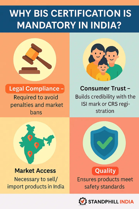
BIS (Bureau of Indian Standards) is the national body responsible for establishing product quality and safety standards in India. Under the BIS Act, 2016, products that fall under specific categories must be certified before they can be manufactured, imported, or sold in the Indian market.
Key Reasons for Mandatory Certification:
Legal Requirement: As of 2025, more than 679 product categories require BIS certification. Non-compliance can lead to product seizure, heavy penalties, or legal action.
Consumer Protection: BIS ensures that Indian consumers are not exposed to unsafe, substandard, or poor-quality products.
Customs Clearance: Without BIS certification, your shipment may be rejected at ports, delaying your business operations.
For the latest list of mandatory products: BIS Product List
✅ Benefits of BIS Certification
📌 1. Legal Compliance
Without BIS certification, selling listed products in India is illegal. This can lead to:
Heavy government penalties
Confiscation of goods
Even imprisonment under severe violations
📌 2. Consumer Trust
Products with the ISI Mark or CRS Registration Number earn greater credibility and trust in the Indian market. It signals to buyers that the product is tested and safe to use.
📌 3. Nationwide Market Access
Certified products can be distributed and sold across India without any legal hurdles, expanding your market reach.
📌 4. Quality Verification
BIS certification guarantees that your product has been tested in BIS-approved labs and complies with Indian standards for safety, durability, and performance.
✅ Why Choose Standphill India as Your BIS Consultant?
With over 20 years of experience and 400+ successful clients, Standphill India offers expert consultancy for all BIS schemes. Here’s why we are the preferred BIS certificate agent in Delhi:
🔹 1. Expertise in All BIS Schemes
We provide end-to-end support in:
CRS Certification (for electronics and IT products)
ISI Mark Certification (for Indian manufacturers)
FMCS Certification (for foreign manufacturers)
Hallmark Registration (for gold/silver jewelry)
LED Product Registration under IS 16103 & IS 10322
🔹 2. Faster Turnaround
Standard BIS approval takes 30–45 working days, but with our streamlined process:
We pre-verify documents
Coordinate with BIS-approved labs
Handle follow-ups with BIS authorities
This reduces delays and increases your chances of first-time approval.
🔹 3. Transparent Pricing
No hidden fees. Our packages start from ₹1.1 lakh for CRS certification and cover:
Documentation
Testing
BIS fees
Consultancy
🔹 4. Dedicated Project Support
You get a single point of contact who provides:
Real-time updates
Status tracking
Personal guidance throughout the process
✅ Step-by-Step BIS Certification Process
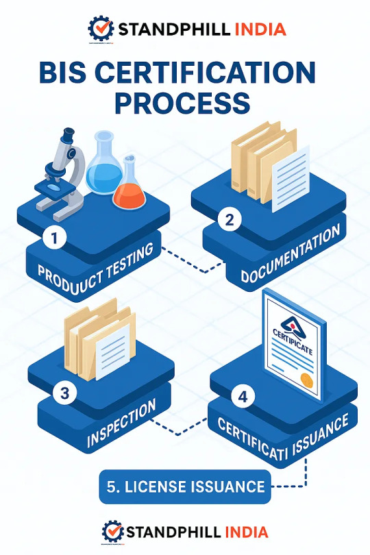
Step 1: Product Evaluation
We analyze your product type and identify the applicable Indian Standards (IS) and appropriate BIS scheme — CRS, ISI, or FMCS.
Step 2: Product Testing
Samples are tested in BIS-recognized NABL-accredited laboratories as per the required IS codes. Pre-testing is done to ensure the product doesn’t fail during official testing.
Step 3: Documentation
Our team prepares and files:
Factory license
Technical layout (e.g., PCB design, circuit details)
Authorized Indian Representative (AIR) documents for foreign clients
Application on the BIS portal
Step 4: BIS Inspection
For schemes like ISI and FMCS, BIS officials visit the manufacturing site for inspection. We assist during audits and handle queries from the BIS authorities.
✅ Step 5: Certification Issuance
Once testing and inspection are successful, BIS issues the license/registration number, which allows you to legally sell the product in India.
✅ BIS Certification for Specific Products
💡 LED Lights
Covered under CRS Scheme
Requires compliance with IS 16103 (Self-ballasted LED lamps) or IS 10322 (Luminaries)
We fast-track testing and ensure correct documentation to avoid rejection
💻 Electronics & IT Goods
Products like laptops, mobile phones, adapters must comply with IS 13252
We help obtain the R-number (CRS Registration Number) for each model
🏗️ Construction Materials
Cement, steel bars, pipes fall under ISI Scheme
BIS approval is mandatory for B2G tenders, exports, and safety assurance
✅ Industries We Serve
Industry | Sample Products |BIS Scheme
Electronics & IT |Mobiles, laptops, chargers |CRS
LED Lighting |LED lamps, luminaires |CRS
Construction |Cement, steel rods, pipes |ISI
Automotive |Helmets, tires, glass | ISI
Jewelry |Gold and silver items |Hallmarking
Household Items |Heaters, kitchen appliances | CRS / ISI
✅ Frequently Asked Questions (FAQs)
❓ How long does BIS certification take?
Typically 20–45 working days, depending on documentation accuracy and product category.
❓ How long is the certificate valid?
Most BIS certificates are valid for 2 years and are renewable without retesting, provided there are no product changes.
❓ Can traders apply for BIS certification?
No. Only manufacturers (domestic or foreign) can apply. Foreign companies must appoint an Authorized Indian Representative (AIR).
❓ What happens if my product fails in BIS testing?
We assist in identifying the failure points, recommend technical corrections, and reinitiate testing to ensure compliance.
📞 Contact the Top BIS Certificate Agent in Delhi — Standphill India
Let our experts take care of the paperwork, testing, and approvals while you focus on your business.
✅ 20+ Years of Experience
✅ Trusted by 400+ Clients Globally
✅ Quick Turnaround Time
✅ No Hidden Fees
📞 Call Now: +91–85279 30453 📧 Email: [email protected] 🌐 Website: www.standphillindia.in
#BISCertificate#BISAgent#BestBISAgent#DelhiBISAgent#StandphillIndia#CompleteGuide2025#CertificationProcess#BISCertification#DelhiIndia#BusinessGrowth#ComplianceGuide#CertificationExperts#QualityStandards#ISO#RegulatoryCompliance#BISStandards#CentralIndia#CertificationAgency#BusinessSolutions#2025Guide
0 notes
Text

Developing electronic products in-house can be resource-intensive, requiring specialized skills, tools, and infrastructure. Outsourcing electronic design services offers a smarter alternative, delivering efficiency and cost savings. By partnering with experts, companies gain access to seasoned engineers who bring deep knowledge of circuit design, PCB layout, and system integration. This eliminates the need to hire and train an in-house team, saving significant time and expense.
#electronic design services#electronics product design#wearable medical device#medical device development company#product design electronics#electronic product design
0 notes
Text
0 notes
Text
Top Signal Integrity Testing Tools by BitWise Laboratories

For high-speed electronic designs, BitWise Laboratories offers industry-leading signal integrity testing tools that ensure clean, accurate data transmission. Their advanced equipment—like TDRs, VNAs, and high-bandwidth oscilloscopes—helps engineers detect issues like jitter, crosstalk, and impedance mismatches. With intuitive software and expert support, it enables faster debugging and optimized PCB layouts. Trusted across industries, their tools are essential for maintaining performance in modern digital systems. Choose BitWise Laboratories for reliable, next-gen signal integrity solutions.
For more information
Visit us : https://bitwiselabs.com/
0 notes
Text

Professional PCB Design Services – Fast, Reliable, Affordable! Expert PCB Design Services – Custom, high-quality PCB layouts for all your electronic projects. From schematic to Gerber files, we deliver fast, accurate, and affordable solutions. Contact us for a quote today!
#pcb assembly#iotdevelopment#businessautomation#smartsolutions#softwaredevelopment#techinnovation#iot#pcb#iotsolutions#iot platform
0 notes
Text
Streamlining PCB Layouts with Bay Area Circuits
Bay Area Circuits, a leading PCB company, specializes in delivering high-quality pcb layouts tailored to meet diverse industry needs. With a commitment to precision and innovation, they offer comprehensive pcb layout design services, ensuring optimal performance and reliability for every project. Their expertise extends to utilizing advanced printed circuit board design software, facilitating efficient and accurate design processes. Whether you're developing prototypes or large-scale productions, Bay Area Circuits provides the tools and support necessary for success. Visit Bay Area Circuits today to elevate your PCB design projects with expert solutions!
0 notes
Text
Explore the High-Performance KIA SIP KIA6299H – A Reliable Audio Power Amplifier
When it comes to dependable audio amplification solutions, the KIA SIP KIA6299H stands out as a trusted choice among professionals and electronics enthusiasts alike. Offered in a convenient lot of 2 on Nikkoe.com, this integrated circuit is designed to deliver strong and clear audio signals, making it ideal for a variety of sound-related applications.

What is the KIA SIP KIA6299H?
The KIA6299H is a Single In-line Package (SIP) audio power amplifier developed by KEC. SIP modules like the KIA SIP are known for their compact form factor and efficient pin layout, making them easy to install on PCBs with limited space. The KIA6299H is specifically designed for use in stereo audio amplification, offering high output power with minimal external components.
This IC supports dual-channel output and is commonly used in stereo systems, radios, televisions, and small audio systems. With its built-in thermal shutdown and overvoltage protection, the KIA SIP provides enhanced durability and long-term reliability in electronic circuits.
Key Features of the KIA SIP KIA6299H
Dual Channel Audio Output – Supports stereo output with clear, powerful sound.
Compact SIP Design – The single in-line package allows for easy PCB integration.
Built-in Protections – Includes overvoltage, short circuit, and thermal shutdown features.
High Efficiency – Delivers high output with low distortion and minimal heat generation.
Low Component Requirement – Simplifies circuit design and assembly.
Why Choose the KIA SIP from Nikkoe.com?
When sourcing electronic components, quality and authenticity matter. Nikkoe.com offers a genuine KIA SIP KIA6299H IC in a lot of 2, ensuring you get not only a great price but also reliable performance. Whether you're repairing existing audio systems or designing new ones, this IC provides the trusted performance that engineers have relied on for years.
Additionally, Nikkoe.com offers fast shipping, competitive pricing, and excellent customer service. Buying from a reputable supplier reduces the risk of counterfeit components and ensures your project meets both functional and safety standards.
Applications of the KIA6299H SIP
Thanks to its robust design and efficient performance, the KIA SIP is used in:
Home stereo systems
Portable audio equipment
Television audio output stages
DIY audio amplifier projects
Educational electronics kits
Final Thoughts
If you’re looking for a compact, durable, and efficient audio amplifier IC, the KIA SIP KIA6299H is a top-tier choice. With features that support high-quality audio performance and protection mechanisms for longevity, this IC is perfect for any audio project.
Order your KIA SIP today from Nikkoe.com and experience quality electronics backed by expert service.
0 notes
Text
ASC: The Ultimate Destination for High-Performance Digital PCB and PCB Digital Solutions
In the digital age, the backbone of every advanced electronic device is a reliable and efficient digital PCB. At American Standard Circuits (ASC), we specialize in delivering world-class PCB digital solutions that cater to the needs of innovators across a spectrum of industries. From aerospace and automotive to medical, telecommunications, and green energy, ASC’s commitment to quality, speed, and technical expertise makes us the preferred partner for digital PCB manufacturing and design.

Unmatched Expertise in Digital PCB Manufacturing
ASC’s reputation as a leader in digital PCB manufacturing is built on decades of experience, state-of-the-art facilities, and a relentless pursuit of innovation. We offer a comprehensive range of PCB digital services, from the simplest single-sided boards to intricate multilayer and HDI (high-density interconnect) designs. Our advanced capabilities allow us to support even the most complex digital PCB requirements, ensuring your products are equipped for maximum performance and reliability.
Our digital PCB manufacturing capabilities include:
Multilayer and HDI digital PCB fabrication: Up to 40+ layers for sophisticated electronic systems.
Controlled impedance and high-speed signal management: Critical for data-intensive and high-frequency digital applications.
Blind, buried, and microvias: Enabling compact, space-saving PCB digital layouts.
Conductive and non-conductive via filling: Supporting advanced circuit design and reliability.
Edge plating, castellations, and custom finishes: For specialized connectivity and enhanced durability.
Lead-free and RoHS-compliant processes: Meeting global environmental and safety standards.
We partner with top-tier material suppliers such as Isola, Nelco, Panasonic, Shengyi, and Taconic, ensuring every digital PCB we produce meets the highest industry standards.
Rapid Turnaround and Certified Quality
At ASC, we understand that speed is essential in bringing your innovations to market. That’s why we offer quick-turn digital PCB services, with some projects completed in as little as 24 hours. Our robust quality assurance program is backed by Class III and MIL certifications, making us a trusted supplier for mission-critical applications where failure is not an option.
Every PCB digital solution undergoes rigorous inspection and testing, guaranteeing reliability, performance, and consistency. Our commitment to quality means you can trust ASC to deliver digital PCBs that exceed your expectations.
End-to-End Support and Engineering Excellence
From initial concept to final delivery, ASC’s team of digital PCB experts is dedicated to your success. We provide comprehensive engineering support, including design-for-manufacturability (DFM) reviews, material selection guidance, and rapid prototyping. Our responsive customer service ensures that most technical questions are answered immediately, helping you avoid costly delays and keep your project on track.
Serving a Wide Range of Industries
ASC’s digital PCB and PCB digital solutions are integral to the success of companies in:
Aerospace & Defense: Certified, rugged digital PCBs for high-reliability environments.
Automotive: Advanced PCB digital systems for next-generation vehicles.
Medical: Precision digital PCBs for diagnostic, imaging, and monitoring equipment.
Telecommunications: High-frequency, high-speed digital PCB solutions for modern networks.
Industrial & Green Energy: Durable and efficient digital PCBs for automation and sustainable energy systems.
Choose ASC for Your Digital PCB Needs
When you choose ASC, you’re partnering with a leader in digital PCB and PCB digital innovation. Our advanced manufacturing capabilities, certified processes, and experienced team ensure your digital PCB projects are completed on time, within budget, and to your exact specifications.
0 notes
Text
A Comprehensive Guide to Circuit Board Manufacturing: From Design to Production
Circuit board manufacturing is the backbone of modern electronics. Whether it's your smartphone, car dashboard, or industrial machine—every electronic device begins with a printed circuit board (PCB). In this guide, we’ll walk through the complete journey of pcb manufacturing, from design to final production, in a simple and easy-to-understand way.
Step 1: PCB Design and Layout
The process begins with a schematic diagram, which is turned into a layout using CAD software.
Engineers choose materials, layer stack-ups, and routing paths based on the product's function.
Design for manufacturability (DFM) checks are done to ensure the design can be produced efficiently using standard Electronics Manufacturing Services.
Step 2: Preparing the Raw Materials
Copper-clad laminates are the base materials used in pcb manufacturing.
These are cleaned and prepped to ensure they bond well with photoresist and other layers.
Step 3: Imaging and Etching
A light-sensitive film (photoresist) is applied to the copper surface.
UV light is used to expose the circuit pattern onto the board.
Unwanted copper is removed using a chemical etching process, leaving behind the desired tracks for circuit board manufacturing.
Step 4: Drilling and Plating
Precise holes are drilled for component leads and inter-layer connections (vias).
These holes are then plated with copper to create electrical pathways between layers.
Need reliable Electronics Manufacturing Services that deliver precision in every layer? Partner with experts who follow global production standards.
Step 5: Solder Mask and Surface Finish
A protective solder mask is applied over the board to prevent oxidation and short circuits.
Finishes like HASL, ENIG, or OSP are added to the pads to improve solderability.
Step 6: Silkscreen and Final Fabrication
Labels, part numbers, and symbols are printed using silkscreen to assist during component assembly.
The boards are then cut into their final shape using CNC routers or V-cut machines.
Step 7: Electrical Testing and Quality Inspection
Each PCB goes through electrical testing to ensure there are no open or short circuits.
Visual inspections and automated tools are used to check for any surface defects or misalignments.
Quality control is critical at every stage of circuit board manufacturing to ensure high performance.
Conclusion
Understanding the full process of pcb manufacturing helps you make better decisions when choosing the right Electronics Manufacturing Services. From detailed design to strict quality checks, every step matters in ensuring the reliability and function of your electronics. High-quality circuit board manufacturing is key to a successful end product.
Upgrade your electronics with trusted Electronics Manufacturing Services for flawless circuit board production.
Also read:-
Top Trends Shaping the Future of Electronics Manufacturing Services in 2025
0 notes
Text
How to Overcome Common Challenges in PCB Assembly for ESDM Projects

In the dynamic world of Electronics System Design and Manufacturing (ESDM), success hinges not just on innovation, but also on precise execution—especially during PCB (Printed Circuit Board) assembly. As projects become more complex, so do the challenges faced during this critical phase. At Aimtron, we’ve seen firsthand how addressing these challenges early leads to smoother project flows, faster time-to-market, and higher quality products.
In this blog, we’ll dive into the most common PCB assembly challenges for ESDM projects and share proven strategies to overcome them.
1. Component Sourcing and Availability
The Challenge: Global supply chain disruptions, component shortages, and long lead times can delay PCB assembly, jeopardizing project timelines.
The Solution:
Early BOM Finalization: Lock your Bill of Materials (BOM) early and validate components for availability.
Multiple Sourcing Strategies: Partner with trusted suppliers and maintain alternate part options.
Inventory Management: Use just-in-time (JIT) inventory systems while keeping a buffer for critical components.
Leverage Aimtron’s Global Network: Our established supplier partnerships help mitigate shortages and ensure timely procurement.
2. Design for Manufacturability (DFM) Issues
The Challenge: PCBs designed without considering manufacturing capabilities often lead to rework, delays, and higher costs.
The Solution:
Early DFM Review: Engage manufacturing experts during the design phase for feedback on layout, spacing, and assembly feasibility.
Simulation and Validation: Use advanced tools to simulate manufacturing processes.
Collaboration with Aimtron's Engineering Team: Our design-for-assembly (DFA) and DFM services ensure your PCB designs are optimized for production from day one.
3. Soldering Defects
The Challenge: Soldering errors like cold joints, bridging, and voids can compromise the reliability of PCBs.
The Solution:
Precision Process Control: Strictly monitor solder paste application, reflow profiles, and hand-soldering techniques.
Quality Training: Continuous training of assembly staff in IPC standards.
Automated Optical Inspection (AOI): Aimtron uses AOI and X-ray inspection systems to detect and correct soldering issues in real-time.
4. Electrostatic Discharge (ESD) Damage
The Challenge: ESD can silently destroy sensitive electronic components during handling and assembly.
The Solution:
Strict ESD Protocols: Implement ESD-safe workstations, grounding systems, and employee training.
Continuous Monitoring: Use ESD monitoring devices to ensure protection throughout the facility.
Certified ESD-Safe Facilities: At Aimtron, our facilities meet global ESD standards to protect your PCBs during every step of assembly.
5. Maintaining Quality in High-Mix, Low-Volume Production
The Challenge: ESDM often requires the assembly of many different PCBs in small batches, making consistency a challenge.
The Solution:
Flexible Manufacturing Systems: Deploy agile production lines capable of quick changeovers.
Strong Documentation Practices: Use detailed work instructions and traceability systems.
Continuous Improvement Programs: Aimtron’s commitment to Kaizen ensures quality is never compromised, no matter the batch size.
6. Thermal Management During Assembly
The Challenge: Components that generate significant heat or require special handling (e.g., BGAs, high-power ICs) can complicate the assembly process.
The Solution:
Proper Heat Profiling: Develop accurate reflow oven profiles tailored to PCB thermal characteristics.
Use of Thermal Reliefs: Design PCBs with thermal relief pads to assist in proper soldering.
Thermal Simulation: At Aimtron, we utilize advanced modeling to predict and manage thermal challenges during assembly.
Conclusion
Navigating the complexities of PCB assembly in ESDM projects requires more than technical know-how—it demands a strategic, proactive approach. From sourcing components to ensuring ESD protection and optimizing for manufacturability, every step is critical.
At Aimtron, we don’t just assemble PCBs—we partner with you to engineer success at every stage of your ESDM journey. By combining cutting-edge technology, global resources, and a deep commitment to quality, we help you overcome challenges and deliver products that meet and exceed market expectations.
Need support for your next ESDM project? Contact Aimtron today and experience the difference that expertise makes.
#PCB Assembly#ESDM#Electronics System Design and Manufacturing#PCB Assembly Services#PCB Assembly Solutions#PCB Design
0 notes