#diode principle
Explore tagged Tumblr posts
Visit Tumblr Blog
Explore Tumblr blogs with no restrictions, modern design and the best experience.
Last Seen Tumblr Blogs


Fun Fact
25% of US internet users with an annual income of $80-100K use Tumblr.
Text
Diode Working....
#diodeworking #diodeworkingprinciple #diodeworkinginhindi #zenerdiodeworkingandconstruction #diodetypesandworking #pnjunctiondiodeworkingandvicharacteristics #whatisdiodeandworking #phonereparing #phonerepairingvideo #phonerepairing #phonerepairingcourse #phonerepairingbusiness #phonerepairingtools #phonerepairingshortvideo #phonerepairingcourseinhindi
#diodeworking #diodeworkingprinciple #diodeworkinginhindi #zenerdiodeworkingandconstruction #diodetypesandworking #pnjunctiondiodeworkingandvicharacteristics #whatisdiodeandworking #phonereparing #phonerepairingvideo #phonerepairing #phonerepairingcourse #phonerepairingbusiness #phonerepairingtools #phonerepairingshortvideo #phonerepairingcourseinhindi
#diode working#diode#pn junction diode#zener diode#schottky diode working#diodes#how does a diode work#diodes explained#diode types#pn junction diode working#working of a diode#schottky diode#zener diode working principle#working of pn junction diode#diode bridge#working principle of varactor diode#varactor diode construction and working#how do diodes work#diode principle#what is a diode#how diodes work
0 notes
Text

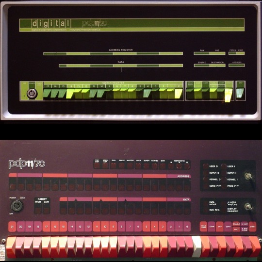


🎄💾🗓️ Day 4: Retrocomputing Advent Calendar - The DEC PDP-11! 🎄💾🗓️
Released by Digital Equipment Corporation in 1970, the PDP-11 was a 16-bit minicomputer known for its orthogonal instruction set, allowing flexible and efficient programming. It introduced a Unibus architecture, which streamlined data communication and helped revolutionize computer design, making hardware design more modular and scalable. The PDP-11 was important in developing operating systems, including the early versions of UNIX. The PDP-11 was the hardware foundation for developing the C programming language and early UNIX systems. It supported multiple operating systems like RT-11, RSX-11, and UNIX, which directly shaped modern OS design principles. With over 600,000 units sold, the PDP-11 is celebrated as one of its era's most versatile and influential "minicomputers".
Check out the wikipedia page for some great history, photos (pictured here), and more -
And here's a story from Adafruit team member, Bill!
The DEC PDP-11 was the one of the first computers I ever programmed. That program was 'written' with a soldering iron.
I was an art student at the time, but spending most of my time in the engineering labs. There was a PDP-11-34 in the automation lab connected to an X-ray spectroscopy machine. Starting up the machine required toggling in a bootstrap loader via the front panel. This was a tedious process. So we ordered a diode-array boot ROM which had enough space to program 32 sixteen bit instructions.
Each instruction in the boot sequence needed to be broken down into binary (very straightforward with the PDP-11 instruction set). For each binary '1', a diode needed to be soldered into the array. The space was left empty for each '0'. 32 sixteen bit instructions was more than sufficient to load a secondary bootstrap from the floppy disk to launch the RT-11 operating system. So now it was possible to boot the system with just the push of a button.
I worked with a number DEC PDP-11/LSI-11 systems over the years. I still keep an LSI-11-23 system around for sentimental reasons.
Have first computer memories? Post’em up in the comments, or post yours on socialz’ and tag them #firstcomputer #retrocomputing – See you back here tomorrow!
#dec#pdp11#retrocomputing#adventcalendar#minicomputer#unixhistory#cprogramming#computinghistory#vintagecomputers#modulardesign#scalablehardware#digitalcorporation#engineeringlabs#programmingroots#oldschooltech#diodearray#bootstraploader#firstcomputer#retrotech#nerdlife
291 notes
·
View notes
Text
Tesla’s Genius: Direct Current Without a Commutator!

In 1888, Tesla made waves by patenting his alternating current (AC) system, which proved far superior to Thomas Edison’s direct current (DC) for long-distance power transmission. The real kicker? He did it without a commutator. This clunky mechanical device was used to reverse the current direction to make DC flow in one direction, but it was notoriously unreliable, prone to wear, and inefficient. Tesla sidestepped this by using high-frequency AC and a rotating magnetic field to generate a more reliable current without the mechanical hassle. After revolutionizing AC with his commutator-free approach, Nikola Tesla wasn’t ready to rest on his laurels. He turned his attention to a new challenge that many physicists of his day thought was impossible: creating direct current (DC) without using a commutator. As always, Tesla wasn’t concerned with traditional boundaries; he was determined to push the limits of what was thought possible.
Tesla’s Ingenious Method
In 1889, Tesla took things even further with a groundbreaking idea. He proposed a method to produce DC without using a commutator. He described how he “sifted” the alternating current into different branches of the circuit. Here’s how he did it:
1. Sifting the Current: Tesla used the concept of directing the AC waves so that the positive and negative halves of the wave were separated. He set up the circuit so that AC waves of one sign (positive or negative) would pass through one branch, while the waves of the opposite sign would go through another. This separation allowed him to create smooth, continuous DC from the AC input.
2. Electrical and Electromagnetic Methods: Tesla proposed two main methods for achieving this. One involved using electrical devices like batteries to create a counteracting electromotive force, which would oppose the AC waves and help separate them. The other method used electromagnetic fields to create active opposition within the circuit, guiding the AC waves into different branches.
3. Magnetic Method: Another method Tesla described used strong permanent magnets and soft iron or steel laminations. By carefully calculating the amount of magnetic metal, Tesla created a setup where the magnetic field interacted with the AC in such a way that allowed continuous currents to be extracted.
Historical Context
Here’s an important note: While Tesla did indeed demonstrate a method for converting AC to DC without a commutator, it’s crucial to understand the broader historical context. Rectification methods—both mechanical and electronic—developed independently over time and were not solely based on Tesla’s innovations. It wasn’t until more than a decade later that practical AC-to-DC conversion technologies, such as vacuum tubes and silicon diodes, became mainstream.
Tesla’s approach did, however, lay the groundwork for modern power electronics by eliminating the need for mechanical parts, making DC conversion more efficient and durable. The principles he introduced continue to influence technologies we use today, from phone chargers to large-scale industrial power systems.
So, the next time you plug in your phone or marvel at the sleek electronics in your home, remember that Tesla’s 1889 breakthrough was a significant step forward. It’s just another example of how Nikola Tesla was light-years ahead of his time!
44 notes
·
View notes
Text
Let me start with the following principle: “Energy is the only universal currency: One of its many forms must be transformed to get anything done.” Economies are just intricate systems set up to do those transformations, and all economically significant energy conversions have (often highly undesirable) environmental impacts. Consequently, as far as the biosphere is concerned, the best anthropogenic energy conversions are those that never take place: No emissions of gases (be they greenhouse or acidifying), no generation of solid or liquid wastes, no destruction of ecosystems. The best way to do this has been to convert energies with higher efficiencies: Without their widespread adoption (be it in large diesel- and jet-engines, combined-cycle gas turbines, light-emitting diodes, smelting of steel, or synthesis of ammonia) we would need to convert significantly more primary energy with all attendant environmental impacts.
Conversely, what then could be more wasteful, more undesirable, and more irrational than negating a large share of these conversion gains by wasting them? Yet precisely this keeps on happening—and to indefensibly high degrees—with all final energy uses. Buildings consume about a fifth of all global energy, but because of inadequate wall and ceiling insulation, single-pane windows and poor ventilation, they waste at least between a fifth to a third of it, as compared with well-designed indoor spaces. A typical SUV is now twice as massive as a common pre-SUV vehicle, and it needs at least a third more energy to perform the same task.
The most offensive of these wasteful practices is our food production. The modern food system (from energies embedded in breeding new varieties, synthesizing fertilizers and other agrochemicals, and making field machinery to energy used in harvesting, transporting, processing, storing, retailing, and cooking) claims close to 20 percent of the world’s fuels and primary electricity—and we waste as much as 40 percent of all produced food. Some food waste is inevitable. The prevailing food waste, however, is more than indefensible. It is, in many ways, criminal.
Combating it is difficult for many reasons. First, there are many ways to waste food: from field losses to spoilage in storage, from perishable seasonal surpluses to keeping “perfect” displays in stores, from oversize portions when eating outside of the home to the decline of home cooking.
Second, food now travels very far before reaching consumers: The average distance a typical food item travels is 1,500 to 2,500 miles before being bought.
Third, it remains too cheap in relation to other expenses. Despite recent food-price increases, families now spend only about 11 percent of their disposable income on food (in 1960 it was about 20 percent). Food-away-from-home spending (typically more wasteful than eating at home) is now more than half of that total. And finally, as consumers, we have an excessive food choice available to us: Just consider that the average American supermarket now carries more than 30,000 food products.
Our society is apparently quite content with wasting 40 percent of the nearly 20 percent of all energy it spends on food. In 2025, unfortunately, this shocking level of waste will not receive more attention. In fact, the situation will only get worse. While we keep pouring billions into the quest for energy “solutions”—ranging from new nuclear reactors (even fusion!) to green hydrogen, all of them carrying their own environmental burdens—in 2025, we will continue to fail addressing the huge waste of food that took so much fuel and electricity to produce.
20 notes
·
View notes
Text
Ratthi shone like a diode in a hotel wall display—bright and irritating. G53U had sealed it on the first day at the hotel with wound sealant from his medkit. But you couldn’t seal Ratthi that easily. He crackled with an aura of condescension, reminding G53U that he could now do whatever he wanted and that his augmentation wasn’t a problem; they still considered him human. G53U was used to reading what lay behind the words. You couldn't survive without it. If people were honest about everything, they’d get into trouble, so they developed their own language, hiding the truth behind enthusiastic phrases. And they knew how to hear the truth when necessary. You couldn't live without it either; you needed to know where trouble was coming from. There had been an incident at the factory, a minor equipment failure = some shit has spiraled out of control, resulting in casualties. An investigation is underway = everyone needed to keep a low profile; random executives would be blamed. The best course of action in that case was to get damaged and visit the medical center with a sick leave slip from yesterday. The situation is under control = run! And now, he was hearing something completely different from what Ratthi was saying. “Augmentation is a major issue. We have no idea what we're going to do with you or who we think you are. You’ll be given options, and you'd better take them. You'll probably end up maintaining bots. There aren’t many, but some haven’t done maintenance in 50 years. You’re almost a bot yourself, so you’ll fit right in.” G53U agreed with all of this in principle. He squinted sleepily at the sun, dead tired of feigning enthusiasm. “What if I choose science? What will they do to me?” “Probably give you a chair? Or a whole department?” Ratthi’s sarcasm was murderous. Okay, G53U was willing to communicate with bots. They tell the truth right off the bat. It must hurt less
9 notes
·
View notes
Text
How a Computer Works - Part 3 (Miniaturization and Standardization)
For anyone just joining in, I'm writing a series of posts explaining perhaps haphazardly all there is to know about how a computer works, from the most basic fundamental circuitry components to whatever level of higher functionality I eventually get to. As explained in the first post on this subject, I am doing this just in pure text, so that if you are inclined you can straight up print these posts out or narrate them onto some audio tape or whatever and have full access to them should every computer in the world suddenly collapse into a pile of dust or something. Part 1 mainly covered the basic mechanical principles of circuitry and how to physically construct a logic gate. Part 2 covered logic gates in detail and how to use them to create a basic working architecture for a general purpose computer. Today we're going to be talking more about what you're looking at when you crack a machine open so you can make sense of all the important fiddly bits and have maybe a starting point on how to troubleshoot things with a multimeter or something.
Before getting into it though, I do have to shake my little donation can again and remind you that I do not know how I am going to get through the winter without becoming homeless, so if this is valuable to you, I'd appreciate some help.
Boards of Bread and Printed Circuits
With the things I've explained so far, you could totally build a computer right now, but it'd be a bit messy. You can totally buy resistors, transistors, capacitors, and diodes by the bagful for basically nothing, and cheap rolls of insulated wire, but there's all these long exposed pins to cut short and soldering things in mid-air is a messy nightmare and you'd just have this big tangle of wires in a bag or something that would almost certainly short out on you. So let's look into ways to organize stuff a little.
If you start playing around with electronics on your own, one of the first things you want to hook yourself up with besides raw components and wires is a breadboard or 12. And if you're watching people explain these things with visual aids, you'll also see a lot of them, so it's good to know exactly what they are and how they work. Your standard breadboard is a brick of plastic with a bunch of little holes in it. Incidentally, the name comes from how the first ones were literally just named after the wooden cutting boards for slicing bread people recycled to make them. Inside these holes there's some pinching bits of conductive metal which connect to each other in a particular way (pretty sure you can just see the strips that connect one if you pry the bottom off), so you can just jam a thing wire or prong into a hole, have it held in place, and make a connection to every other hole its connected to on the other side.
There is a ton of standardization to all of this. The holes should always be 0.1 inches apart () and split into two big grids. Everyone I've ever seen has 63 rows, each with 5 holes labeled A-E, a shallow channel through the middle of the board, and then another 5, F-J, and we generally have numbers printed every 5 rows. Down underneath, for any given row, the set of 5 pins on each side of the channel are connected. So, holes 1A, 1B, 1C, 1D, and 1E are all connected to each other, and nothing else. Holes 1F, 1G, 1H, 1I, and 1J are also connected to each other. There's no connection though between 1E and 1F, or 1A and 2A.
Most breadboards will also have a couple of "power rails" along the sides. These are just going to be labeled with a long red line and +, and a long blue or black line and -, and have holes in 2x5 blocks staggered out. With these, all 25 or 50 or whatever holes near the red + line connect with each other, and all the ones near the black line connect with each other. The gaps every 5 holes don't serve any purpose beyond looking different enough from the big grid so you hopefully don't mix it up and forget that these ones all connect down the length, and not in in little clumps across the width like everything else. The idea, for the sake of convention, is you plug a wire connected directly to the positive side of your battery or DC adapter or whatever into any red line hole, the negative side to any blue/black hole, and then tada, you can make a circuit just by plugging a wire in from red to a normal grid line, whatever bits you want span from that grid line to another, and eventually you connect the far end back anywhere on the black/blue line.
With a nice circuit board, there's also little snap-together pegs along the sides, and the power rails are just snapped on with those. So you can just kinda cut through the backing with a knife or some scissors, snap those off, connect multiple boards together without redundant power rails in the middle, and then just have these nice spare long lines of linked sockets. In the computer I'm building on these, I'm just using spare power rails for the bus. Oh and the big grooved channel down the middle also has a purpose. Bigger electronic components, like our good good friend the integrated circuit, are generally designed to be exactly wide enough (or more, but by a multiple of 0.1 inches) to straddle that groove as you plug their legs into the wires on either side, so they nicely fit into a breadboard, and there's a handy gap to slide something under and pry them off later on.
Typically though, you don't see breadboards inside a computer, or anything else. They're super handy for tinkering around and designing stuff, but for final builds, you want something more permanent. Usually, that's a printed circuit board, or PCB. This is pretty much what everyone's going to picture when they think about the guts of a computer. A big hard (usually) green board with a bunch of intricate lines, or "traces" running all over made of (usually) copper. And maybe with some metal ringed holes punched all the way through (they call those vias). These tend to look really complicated and maybe even a little magical, but they're honestly they're just pre-placed wires with a sense of style.
Most of the material of the board is insulated. The copper traces conduct real well, and manufacturers have done the math on just how close together they can be run without connecting to each other in places you don't want. The holes that go all the way through are for either plugging other bits in that tend to come with long legs you maybe want to keep intact, or just ways to run a trace through to the other side, where we often have traces on the back too to maximize our space. Most of what makes them look all cool and magical is how the traces run as close packed as possible to conserve space, and tend to only turn at 45 degree angles, which is just an artifact of how the machinery used to etch them out sued to be iffy about anything else.
So tada, you have all your wires pre-stuck to a nice sturdy board, and maybe even have labels printed right on there for where you solder all the various components to finish the thing. Oh and when you hear people talk about like, motherboards and daughterboards? The big main board you have for everything is a motherboard. Sometimes you need more than that, so you make smaller ones, and connect them up ether with some soldering or cartridge style with end-pins sliding snugly into sockets, and those we call daughterboards.
Integrated Circuits, or as they're also known, "chips"
The last thing you're likely to find if you crack open a computer, or just about any other electronic device that isn't super old or super super simple, are integrated circuits. Generally these are think black plastic bars that look like you'd maybe try to awkardly use them to spread cheese or peanutbutter on crackers in a prepacked snack or something, with rows of tiny little legs that running along either side. Kinda makes them look like little toy bugs or something. Sometimes they're square with pins along every edge, because sometimes you need a lot of pins. These are integrated circuits, or microchips, or just chips, and wow are they handy.
Sometime back in the 60s when people were really getting their heads around just how ridiculously small they could make electronic components and still have them work, we started to quite rapidly move towards a point where the big concern was no longer "can we shrink all this stuff down to a manageable size" and more "we are shrinking everything down to such an absurdly tiny size that we need to pack it all up in some kind of basically indestructible package, while still being able to interact with it."
So, yeah, we worked out a really solid standard there. I kinda wish I could find more on how it was set or what sort of plastic was used, but you take your absurdly shrunken down complex circuit for doing whatever. You run the teensiest tiniest wires you can out from it that thicken up at the ends into standard toothy prongs you can sink into a breadboard or a PCB with that standardized pin spacing, and you coat it all in this black plastic so firmly enveloping it that nothing can move around inside or get broken, hopefully.
And honestly, in my opinion, this is all TOO standardized. The only real visible difference between any two given integrated circuits is how many legs they have, and even those tend to come to some pretty standard numbers. They're always the same size shape and color, they all have the same convention of having a little indented notch on one side so you know which end is which, and they all seem to use just the worst ink in the world to print a block of numbers on the back with their manufacturer, date of assembly, a catalog number, and some other random stuff.
For real if there's any real comprehensive standard for what's printing on these, I can't for the life of me find it. All I know is, SOMEWHERE, you've got a 2 or 3 letter code for every manufacturer, a number for the chip, and a 4 digit date code with the last 2 digits of the year, and which week of that year it was. These three things can be in any order, other things can also be on there, probably with zero spacing, and usually printed in ink that wipes away like immediately or at least is only readable under really direct light, it sucks.
Once you know what a chip is though and look up the datasheet for it, you should have all sorts of handy info on what's inside, and just need to know what every leg is for. For that, you find which end has a notch in it, that's the left side, sometimes there's also a little dot in the lower left corner, and hopefully the label is printed in alignment with that. From there, the bottom left leg is pin 1, and then you count counterclockwise around the whole chip. You're basically always going to have positive and negative power pins, past that anything goes. You can cram a whole computer into a single chip, yo can have someone just put like 4 NAND gates on a chip for convenience, whatever.
OK, but how do they make them so small?
OK, so, mostly a circuit we're going to want to shrink down and put on a chip is just gonna be a big pile of logic gates, we can make our logic gates just using transistors, and we can make transistors just by chemically treating some silicon. So we just need SUPER flat sheets of treated silicon, along with some little strands of capacitive/resistive/insulating material here and there, and a few vertically oriented bits of conductive metal to pass signals up and down as we layer these together. Then we just need to etch them out, real real small and tight.
And we can do that etching at like, basically infinite resolution it turns out. It just so happens we have access to special acids that eat through the materials we need them to eat through, but that only work when they're being directly hit with fairly intense UV light. And a thing about light is when you have say, a big cut out pattern that you hold between a light and a surface, it casts a shadow on it... and the scaling of that shadow depends entirely on the distances between the light, the pattern, and the surface. So if you're super careful calibrating everything, you can etch a pattern into something at a scale where the main limiting factors become stuff like how many molecules thick things have to be to hold their shape. Seriously, they use electron microscopes to inspect builds because that's the level of tininess we have achieved.
So yeah, you etch your layers of various materials out with shadow masks and UV acid, you stack them up, you somehow align microscopic pins to hold them together and then you coat the whole mess in plastic forever. Tada. Anything you want in a little chip.
ROMs, maybe with various letters in front
So there's a bunch of standard generally useful things people put into ICs, but also with a computer you generally want some real bespoke stored values with a lookup table where you'll keep, say, a program to be run by feeding whatever's inside out to the bus line by line. For that we use a chip we call Read Only Memory, or ROM. Nothing super special there, just... hard wire in the values you need when you manufacture it. Manufacturing these chips though is kind of a lot, with the exacting calibrations and the acid and the clean rooms and all. Can't we have some sort of Programmable ROM? Well sure, just like build it so that all the values are 1, and build a special little thing that feeds more voltage through than it can handle and physically destroy the fuse for everything you don't want to be a 1.
OK that's still kind of a serious commitment. What if I want to reuse this later? Oh, so you want some sort of Erasable PROM? OK someone came up with a funky setting where you overload and blow out the fuses but then if you expose the guts of the chip to direct UV light through this little window, everything should reform back to 1. Just like, throw a sticker on there when you don't want to erase it. Well great, but can we maybe not have me desolder it and take it out to put under a lamp? Oh la de da! You need Electronically Erasable PROMs? EEPROMs? I guess we can make THAT work, somehow. They're still gonna be slow to write to though, can't have anything. I mean, not unless we invented like, flash memory. Which somehow does all this at speeds where you can use it for long term storage without it being a pain. So that's just kinda the thing we have now. Sorry I don't quite get the principles behind it enough to summarize. Something about floating components and needing less voltage or whatever. Apparently you sacrifice some read speed next to older options but hey, usable rewritable long term storage you just plug in, no jumping through extra hoops.
So OK. I think that's everything I can explain without biting the bullet and explaining ALUs and such. Well, there's keyboards (they're just buttons connecting input lines), monitors (these days, LEDs wired up in big grids), and mice (there's spokes in wheels that click X times or cameras checking the offset values of dust on your desk or whatnot).
Maybe throw me some money before we move on ?
CONTINUED IN PART 4
#computers#computer science#pcb#printed circuit board#integrated circuits#microchip#breadboards#education#electronics
56 notes
·
View notes
Text

Sustainable, manganese-based phosphors show promise for white-light LEDs
Virtually all light-emitting diodes used today require phosphors based on so-called rare-earth elements, which are expensive and challenging to obtain. In a collaborative research project between Heinrich Heine University Düsseldorf (HHU) and the University of Innsbruck, chemists have now demonstrated that the element manganese is in principle also suitable for such applications. In their study published in the journal Angewandte Chemie International Edition, they show that this approach enables white light to be generated from a single manganese-based phosphor. Light-emitting diodes (LEDs) are energy-efficient and flexible, making them a key technology for sustainable lighting. Current white-light LEDs typically comprise a blue semiconductor LED, the light of which is then converted by two layers of photoactive materials into green light and red light. Combining these light colors creates the desired white light.
Read more.
2 notes
·
View notes
Text
How do BMW's new laser headlights work and what advantage do they have over other headlight technologies?
BMW's laser headlights represent a groundbreaking leap in automotive lighting technology, combining advanced physics with intelligent safety systems. Here's a detailed breakdown of their working principles and key advantages over traditional lighting technologies:
1. Core Technology & Working Principle BMW's Laserlight system does not directly project laser beams onto the road but uses lasers to generate intense white light through a multi-stage process:
Laser Activation: Three blue laser diodes (wavelength ~450nm) emit high-intensity beams.
Mirror Reflection: The laser beams are directed through a series of mirrors within the headlamp assembly.
Phosphor Conversion: The blue lasers strike a lens filled with yellow phosphorus, triggering a chemical reaction that converts the light into bright white light (5,500–6,000K color temperature).
Diffusion & Projection: The white light is diffused to reduce glare and projected via a reflector bowl, achieving a focused beam.
This method produces 10x brighter light than LEDs while maintaining safety for human eyes and animals.
2. Key Advantages Over Traditional Technologies Feature Laserlight LED/Other Tech Brightness 600m max range (vs. 300m for LED) Limited by lower lumen density Energy Efficiency 30% less energy than LEDs Higher power consumption Beam Precision Laser-guided adaptive focus Fixed or less dynamic patterns Component Size Diodes 1/100th LED size (10μm) Bulky heat sinks required Lifespan 50,000–100,000 hours 30,000–50,000 hours (LED)
3. Intelligent Safety & Adaptive Features
Anti-Dazzle Control: Infrared cameras detect oncoming traffic and automatically dim/redirect beams.
Dynamic Light Spot: Focuses on obstacles (e.g., pedestrians, animals) up to 300ft (92m) ahead.
GPS-Enabled Steering: Syncs with navigation to pre-illuminate turns.
Speed-Activated Logic: Only activates at >60 km/h to avoid urban glare.
4. Design & Sustainability Benefits
Compact Housing: Smaller components allow sleeker headlight designs (e.g., BMW i8's slim profile).
Heat Management: Minimal heat output reduces cooling demands vs. LED/Xenon.
Material Innovation: Uses 0.7mm hardened glass layers for 50% weight reduction.
5. Limitations & Future Outlook
High Cost: Currently limited to premium models (e.g., X7, 8 Series).
Regulatory Hurdles: Required 7+ years for U.S. road approval.
Emerging Competitors: Audi's DML matrix lights challenge with pixel-level control.
BMW continues refining this technology, with plans to expand it to motorcycles and mid-tier vehicles by 2026. While not replacing LEDs entirely, laserlights redefine nighttime driving safety and efficiency for high-performance applications.

#led lights#car lights#led car light#youtube#led auto light#led headlights#led light#led headlight bulbs#ledlighting#young artist#car culture#cars#race cars#classic cars#car#suv#vehicle#automobile#muscle car#car light#yellow headlights#headlamp#headlight#car lamp#lamp#laser headlights#other headlight#bmw#bmw cars#vintage car
4 notes
·
View notes
Text
Understanding the Functionality of Samsung Refrigerator PCB Main Assembly

Samsung refrigerators have become essential appliances in modern households, offering innovative features and advanced technologies to ensure food preservation and convenience. The (Printed Circuit Board) PCB Main Assembly serves as the brain of the refrigerator, coordinating various functions and ensuring optimal performance.
Components of the Refrigerator PCB Main Assembly
The Refrigerator PCB Main Assembly consists of several essential components, each playing a crucial role in the refrigerator's operation.
Microcontroller: It is the central processing unit (CPU) and the computer performs programmed instructions to coordinate communication between the components.
Sensors: The ambient parameters (temperature, humidity, door status) supply critical information for regulation.
Relays: You control the flow of electricity to the compressor, fan motors, and defrost heater.
Capacitors: It will help you store the electrical energy and help to regulate voltage, and guarantee that the PCB is operating reliably.
Resistors: Protect sensitive components from harm by limiting the flow of electricity across certain circuits.
Diodes: Allow current to flow exclusively in one direction to avoid reverse polarity and safeguard components from damage.
Connectors: Facilitate electrical connections between the PCB and other refrigerator components to ensure seamless integration.
Working Principle PCB Main Assembly
The PCB Main Assembly operates on a set of programmed instructions that determine its behavior depending on sensor input and user command. The micro controller continuously monitors sensor input such as the reading of the temperature from the refrigerator compartment, and freezer. The microcontroller controls the transition of the compressor on, or off or the speed of the fan and also the defrost cycles based on the sensor data as to how to keep the temperature and humidity at the optimal level. In addition to the other refrigerator components, for example, display panel and user interface, the PCB Main Assembly provides feedback and enables users’’ interaction. The PCB Main Assembly incorporates safety features of overload protection and temperature sensors to protect the refrigerator from damage and to protect the user.
Communication Protocols
Data can be communicated to other components through microcontrollers by communication protocols like UART (Universal Asynchronous Receiver Transmitter), SPI (Serial Peripheral Interface), and I2C (Inter Integrated Circuit).
UART is used to transfer real-time data from a microcontroller to external devices like display panels and temperature sensors.
There is a power of communication SPI and I2C for the communication of integrated circuits associated with the PCB Main Assembly for efficient data transfer and synchronization between components.
Troubleshooting and Maintenance
Common issues with the Samsung Refrigerator PCB Main Assembly include sensor failures, relay malfunctions, and power supply issues, which can affect the refrigerator's performance.
To solve PCB Main Assembly problems, we can use diagnostic methods, like running self-tests and checking the error code.
The assembly can stay longer depending on the main, such as cleaning dust and debris from the PCB and securing appropriate ventilation.
The PCB Main Assembly is an important component of the Samsung refrigerator systems since it organizes several functions to contribute to the overall efficiency of the refrigerator and food preservation. Fore-knowledge of the PCB Main Assembly and the way it is constructed can assist users in likely managing problems in their fridges.
2 notes
·
View notes
Text
Notes on Class 12 Physics Semiconductor Electronics: Materials, Devices and Simple Circuits
Introduction to Semiconductor Electronics: Materials, Devices, and Simple Circuits
Semiconductor electronics forms the backbone of modern technology, revolutionizing communication, computing, and countless other fields. This branch of physics deals with the study of semiconductor materials, devices, and their applications in electronic circuits. Semiconductors, such as silicon and germanium, play a pivotal role due to their unique properties, which lie between those of conductors and insulators.
In this study, we explore the intricate workings of semiconductor devices like diodes, transistors, and integrated circuits. These devices enable the manipulation, amplification, and regulation of electronic signals, essential for powering electronic gadgets, processing information, and controlling machinery.
Through understanding semiconductor physics, device operation principles, and circuit design techniques, we embark on a journey to comprehend the intricate world of semiconductor electronics. This knowledge not only forms the foundation for advanced studies in electronics but also empowers us to innovate and contribute to the ever-evolving landscape of modern technology.
Here are some notes on Class 12 Physics Semiconductor Electronics: Materials, Devices, and Simple Circuits:
Introduction to Semiconductor Physics:
Semiconductors are materials with electrical conductivity between that of conductors and insulators. Examples include silicon (Si) and germanium (Ge).
Intrinsic semiconductors are pure semiconductors with equal numbers of electrons and holes.
2. Extrinsic Semiconductors:
Doping introduces impurities into semiconductor crystals to modify their conductivity.
N-type semiconductors are doped with materials that increase the number of free electrons.
P-type semiconductors are doped with materials that create electron-deficient holes.
3. PN Junction Diode:
A PN junction diode is formed by joining a P-type semiconductor with an N-type semiconductor.
It allows current to flow in one direction (forward-biased) and blocks it in the other direction (reverse-biased).
Characteristics include forward and reverse biasing, breakdown voltage, and diode equation.
4. Diode Applications:
Rectification: Converting AC to DC using diodes in half-wave or full-wave rectifier circuits.
Clipping and Clamping: Limiting voltage levels in electronic circuits using diodes.
Voltage Regulation: Stabilizing voltage levels using Zener diodes.
5. Transistors:
Bipolar Junction Transistor (BJT) and Field Effect Transistor (FET) are common types.
Transistors amplify or switch electronic signals and can be used as amplifiers, switches, or oscillators.
6. Transistor Configurations:
Common emitter, common base, and common collector configurations for BJTs.
Common source, common gate, and common drain configurations for FETs.
7. Transistor Amplifiers:
Amplifier circuits use transistors to increase the amplitude of electrical signals.
Common emitter and common collector configurations are commonly used for amplification.
8. Logic Gates:
Basic building blocks of digital circuits that perform logical operations (AND, OR, NOT, etc.).
Implemented using transistors to process binary inputs and produce binary outputs.
9. Integrated Circuits (ICs):
ICs are miniaturized electronic circuits fabricated on a single semiconductor chip.
Types include analog ICs (op-amps, voltage regulators) and digital ICs (microprocessors, memory chips).
10. Simple Circuits:
Basic electronic circuits incorporating semiconductor devices like diodes, transistors, and ICs.
Examples include amplifiers, oscillators, timers, and voltage regulators.
Understanding semiconductor electronics is essential for various applications in modern technology, including computers, telecommunications, and consumer electronics. These notes provide a foundational understanding of semiconductor materials, devices, and circuits, laying the groundwork for further exploration in the field of electronics.
1 note
·
View note
Text
This post has enough notes that someone else already sais this, but something really fascinating i find about electrical components is how a bunch of them are jist pairs of the same thing, but with the input and outputs switched
For example, an electric turbine and an electric motor are basically the same thing. Sure, they are each optimised for their use, but they use the exact same principle. One uses mechanical energy to produce electrical energy, and the other one electrical for mechanical.
Then we have solar panels and LEDs. If you shine light into an LED, you can actually measure a current that it produces. And a solar panel can produce *some* light if yoy power it. Theyre both diodes
And again, microphones and speakers. You open them up and theyre basically the same thing
And i juat think that's pretty neat

lil tidbit about Solar
Not a funni comic and a bit nerdy, but i wanted to write about something that i find cool lol.
4K notes
·
View notes
Text
Robot's Nose- Electrochemical Gas Sensor ESD and Surge Protection Solution
Electrochemical gas sensors are devices that measure gas concentration by detecting the current signal generated from oxidation or reduction reactions of target gases on the electrode surface. They play a crucial role in industrial safety, environmental monitoring, indoor air quality assessment, and portable gas detection equipment.
Core Principle
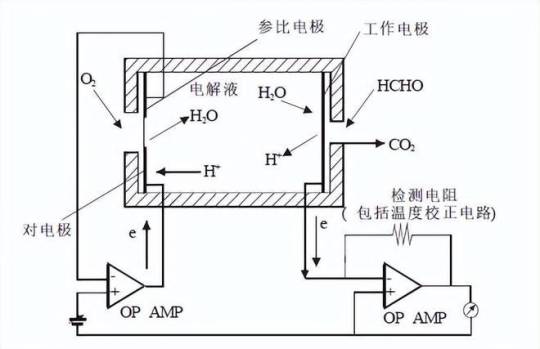

Leiditech’s ESD and Surge Protection Guidelines for Electrochemical Sensor Circuits
1. Sensor Interfaces (WE/CE/RE)
A low-capacitance ESD device (Leiditech SD05C) is connected in parallel. Its bidirectional protection characteristic is compatible with the signal range of the three electrodes, and its low capacitance of 11pF minimizes attenuation of nanoampere-level weak current signals. It ensures that under IEC 61000–4–2 Level 4 tests (±8kV contact discharge, ±15kV air discharge), the clamping voltage remains within 13V, which is lower than the power supply voltage withstand limit of the downstream ADA4505–2 operational amplifier.
2. Potentiostatic Control Module and Transimpedance Amplifier
It is recommended to connect an ESDA05CC (SOD-523 package) in parallel across the feedback network (100kΩ resistor) of the transimpedance amplifier. Its 39pF capacitance matches the circuit’s capacitive reactance characteristics, and its 20A current handling capacity copes with sudden surges, protecting the high-impedance feedback node from ESD breakdown.
3. Signal Output and MCU Interfaces
l On the path where the sensor signal, after amplification, is transmitted to the MCU (e.g., AIN1± pin of AD7798), an RC filter network (1kΩ+100pF) is connected in series. The cutoff frequency of 1.6MHz is compatible with the sensor’s signal bandwidth (≤10Hz). Meanwhile, an ESDA33CP30 (3.3V) or SMDA05CCN (5V) is connected in parallel, both meeting IEC 61000–4–2 Level 4 protection requirements.

4. Power Module

For 3.3V VCC: Leiditech uses ESD0321CW (DFN0603 package, 30pF capacitance, 21A discharge current).

Leiditech Electronics is committed to becoming a leading brand in electromagnetic compatibility (EMC) solutions and component supply. We offer a wide range of products, including ESD, TVS, TSS, GDT, MOV, MOSFET, Zener diodes, and inductors. With an experienced R&D team, we provide personalized customization services to deliver the highest quality EMC solutions tailored to our customers’ needs.
If you’d like to learn more or have any questions, don’t hesitate to reach out:
Visit us at [en.leiditech.com]
#GasSensorProtection #ElectrochemicalSensors #ESDProtection #SurgeProtection #Leiditech #CircuitDesign #IndustrialSafety #EMCsolutions #TechBlog #SensorDesign #IoTDesign #SmartSensors #EmbeddedEngineering #PCBDesignTips
0 notes
Text
Understanding Generator Excitation: A Complete Technical Guide

1. Introduction to Generator Excitation Generator excitation is a fundamental aspect of power generation systems, playing a critical role in regulating voltage and ensuring system stability. Whether in hydroelectric, thermal, or renewable energy plants, excitation systems are essential for the efficient and reliable operation of synchronous generators. This technical guide offers a comprehensive overview of generator excitation, focusing on its principles, components, types, and applications.
2. The Purpose of Generator Excitation Generator excitation refers to the process of supplying a controlled DC current to the rotor winding of a synchronous generator. This excitation current produces the magnetic field necessary for generating electricity. The strength of this magnetic field directly influences the terminal voltage of the generator. By adjusting the excitation current, operators can regulate the output voltage and reactive power flow, which is vital for grid stability and load balancing.
3. Basic Components of Excitation Systems A typical excitation system comprises several core components including the exciter, voltage regulator, and power source. The exciter provides the DC supply to the rotor winding, while the automatic voltage regulator (AVR) continuously monitors and adjusts the excitation current to maintain the desired generator voltage. The power source for the exciter may come from an external DC supply or be derived from the generator itself, depending on the excitation system design.
4. Types of Generator Excitation Systems Generator excitation systems are broadly classified into three main types: static excitation, brushless excitation, and DC excitation.
In static excitation systems, power for the field winding is taken from the generator terminals through a transformer and rectifier setup. This type offers fast response and precise control, making it ideal for modern power plants.
Brushless excitation systems use a small AC generator mounted on the same shaft as the main generator. This exciter produces AC power which is then rectified by rotating diodes and supplied to the rotor winding. The brushless design eliminates the need for slip rings and brushes, thereby reducing maintenance and increasing reliability.
DC excitation systems, although less common in modern setups, use a separate DC generator to supply excitation current. These systems are typically found in older power stations or in applications where simplicity and independence from the main generator are prioritized.
5. Automatic Voltage Regulation and Control The automatic voltage regulator (AVR) is a crucial element of the generator excitation system. It maintains the output voltage within specified limits by adjusting the excitation current in real time. The AVR receives feedback from the generator output and modulates the excitation accordingly to respond to load changes, ensuring consistent voltage supply.
In advanced excitation systems, the AVR is integrated with other control mechanisms such as power system stabilizers (PSS) and protective relays, enhancing the overall stability and performance of the generator under dynamic grid conditions.
6. Importance of Proper Excitation in Power Systems Proper generator excitation is vital for maintaining voltage stability, controlling reactive power, and preventing system disturbances. An inadequately excited generator can lead to voltage fluctuations, increased losses, and even generator damage. In contrast, over-excitation can cause excessive reactive power generation, leading to overvoltage and potential grid instability. Hence, well-designed and precisely controlled excitation systems are indispensable in power plant operations.
7. Applications and Industry Relevance Generator excitation systems are used across various industries, including electric utilities, industrial manufacturing, and renewable energy sectors. Their application spans from small-scale backup generators to large-scale utility power generation units. As grid demands grow and power systems become more dynamic, the role of efficient generator excitation continues to expand, making it a crucial area of focus for engineers and operators.
8. Conclusion In summary, generator excitation is a key technical process that underpins the operation of synchronous generators. From regulating voltage to ensuring system stability, the importance of an effective excitation system cannot be overstated. As power generation technology continues to evolve, the demand for reliable and efficient excitation systems will remain central to the success of modern energy infrastructure. Understanding generator excitation, its types, and its operational significance is essential for anyone involved in the field of power systems and electrical engineering.
Contact Info
2500 State Highway 160, Warrior, AL 35180
Phone: 205-590-3505
Email
Map
https://maps.app.goo.gl/c7y7BLamTPvecBqWA
0 notes
Text
Explosion-Proof Electrical Safety Barrier Market: Technological Innovations and Future Roadmap 2025–2032
Explosion-Proof Electrical Safety Barrier Market, Trends, Business Strategies 2025-2032
Explosion-Proof Electrical Safety Barrier Market size was valued at US$ 187.6 million in 2024 and is projected to reach US$ 267.8 million by 2032, at a CAGR of 4.6% during the forecast period 2025-2032
Our comprehensive Market report is ready with the latest trends, growth opportunities, and strategic analysis https://semiconductorinsight.com/download-sample-report/?product_id=103398
MARKET INSIGHTS
The global Explosion-Proof Electrical Safety Barrier Market size was valued at US$ 187.6 million in 2024 and is projected to reach US$ 267.8 million by 2032, at a CAGR of 4.6% during the forecast period 2025-2032.
Explosion-proof electrical safety barriers are critical components designed to prevent ignition of flammable gases, vapors, or dust in hazardous industrial environments. These devices limit electrical energy to safe levels through intrinsic safety principles, using either Zener diode barriers or galvanic isolation techniques. They find primary application in Zone 0, 1, and 2 hazardous areas as classified by IEC 60079 standards.
The market growth is driven by stringent industrial safety regulations such as ATEX in Europe and NEC in North America, coupled with increasing automation in oil & gas facilities. However, the emergence of alternative protection methods like explosion-proof enclosures presents competitive challenges. Recent technological advancements include smart barriers with IoT-enabled condition monitoring, with companies like Pepperl+Fuchs and Eaton Corporation leading innovation in this space.
List of Key Explosion-Proof Safety Barrier Companies
Pepperl+Fuchs (Germany)
Eaton Corporation (Ireland)
R. STAHL (Germany)
Phoenix Contact (Germany)
PR ELECTRONICS (Denmark)
DATEXEL SRL (Italy)
TURCK (Germany)
Panasonic Eco Solutions (Japan)
FineTek (Taiwan)
Adalet Inc. (U.S.)
Recent competitive dynamics reveal three strategic patterns: established players are divesting non-core safety businesses to focus on explosion-proof technologies, mid-market competitors are forming consortiums to pool R&D resources, and regional specialists are expanding certification portfolios to meet multinational client demands. The market’s technical complexity creates high barriers to entry, but also rewards companies that continuously advance their safety and connectivity features.
Segment Analysis:
By Type
Multi-Channel Segment Leads Due to High Demand in Complex Industrial Setups
The market is segmented based on type into:
Single Channel
Subtypes: Basic, Smart-connected, and others
Multi-Channel
Subtypes: Dual-channel, Four-channel, and others
By Application
Oil and Gas Industry Dominates Due to Stringent Safety Requirements in Hazardous Environments
The market is segmented based on application into:
Oil and Gas
Chemical Processing
Mining
Pharmaceutical
Others
By Technology
Smart Barriers Gain Traction With IoT Integration for Remote Monitoring Capabilities
The market is segmented based on technology into:
Conventional Barriers
Smart Barriers
Subtypes: Wireless-enabled, IoT-connected, and others
By Certification
ATEX-Certified Barriers Lead Due to European Market Dominance
The market is segmented based on certification standards into:
ATEX
IECEx
NEC
Others
Regional Analysis: Explosion-Proof Electrical Safety Barrier Market
North America North America dominates the explosion-proof electrical safety barrier market due to stringent safety regulations, particularly in high-risk industries like oil & gas, chemical processing, and mining. The region’s well-established regulatory framework, including standards set by OSHA (Occupational Safety and Health Administration) and NEC (National Electrical Code), drives the adoption of advanced safety solutions. The United States remains the largest market, accounting for approximately 65% of the regional revenue, with Canada following due to its expanding industrial sector. Investments in digital transformation and industrial automation further stimulate demand for IoT-enabled safety barriers that offer real-time monitoring capabilities. Leading manufacturers like Eaton Corporation and Cooper Crouse-Hinds continue to innovate, focusing on energy efficiency and compliance with ATEX directives.
Europe Europe’s market is characterized by strict compliance requirements under ATEX and IECEx regulations, ensuring high safety standards across hazardous environments. Countries like Germany, France, and the UK lead in adoption due to advanced manufacturing and energy sectors. The EU’s emphasis on Industry 4.0 has accelerated the integration of smart safety barriers capable of predictive maintenance and remote diagnostics. While Western Europe remains the largest consumer, Eastern Europe shows gradual growth, driven by industrial modernization in nations like Poland. Pepperl+Fuchs and R. STAHL are key players, leveraging their expertise to cater to specialized applications such as offshore wind farms and pharmaceutical manufacturing. However, high costs associated with certification and installation pose challenges for SMEs.
Asia-Pacific Asia-Pacific is the fastest-growing market, propelled by rapid industrialization in China, India, and Southeast Asia. China alone contributes over 40% of regional demand, supported by its booming oil & gas and chemical industries. Governments across the region are enforcing stricter workplace safety regulations, spurring the need for explosion-proof solutions. However, price sensitivity leads to a preference for cost-effective, single-channel barriers, particularly in developing markets. Japan and South Korea focus on high-end, multi-channel barriers for precision manufacturing and semiconductor industries. Leading suppliers include Panasonic Eco Solutions and FineTek, who are expanding their distribution networks. The rise of automotive electrification and smart factories further fuels long-term growth prospects.
South America South America presents moderate but steady demand, primarily driven by Brazil’s oil & gas and mining sectors. The region struggles with economic volatility, which limits investments in high-cost safety infrastructure. Local manufacturers often prioritize basic explosion-proof solutions due to budget constraints, while multinational corporations opt for certified ATEX barriers in critical facilities. Argentina and Colombia show nascent growth, supported by small-scale industrial expansions. The lack of uniform safety regulations across countries remains a hurdle, though initiatives like MERCOSUR safety standards aim to harmonize requirements. Partnerships with global players such as TURCK and Phoenix Contact are helping bridge the technology gap.
Middle East & Africa The Middle East’s market is fueled by oil-rich GCC nations (Saudi Arabia, UAE), where stringent safety norms in refineries and petrochemical plants drive adoption. Israel and Turkey are emerging markets due to growing electronics and automotive sectors. Africa faces slower adoption due to limited industrial development, though mining operations in South Africa and Nigeria create localized demand. Infrastructure gaps and lack of skilled labor for installation remain barriers, but foreign investments in energy projects could unlock potential. Companies like Adalet Inc. and DATEXEL SRL are targeting niche applications in desalination plants and LNG facilities, leveraging the region’s energy diversification efforts.
MARKET DYNAMICS
The lack of harmonization between regional certification requirements poses significant hurdles for manufacturers and end-users alike. While ATEX dominates in Europe and NEC in North America, emerging markets often develop their own evolving standards. A single product might require separate certifications for Brazil (INMETRO), Russia (EAC), and China (CCC), each with different testing protocols. This regulatory fragmentation forces manufacturers to maintain multiple product versions, increasing inventory costs by an estimated 15-20%. The challenge intensifies with recent geopolitical shifts, as trade restrictions alter certification reciprocity agreements between regions. Multinational corporations must navigate this complex landscape while ensuring all facilities maintain equivalent safety standards.
Retrofitting Legacy Systems Many industrial facilities operate aging infrastructure where integrating modern safety barriers proves technically challenging and cost-prohibitive. Retrofitting often requires complete electrical system overhauls rather than simple component replacements.
Material Compatibility Issues Certain industrial environments contain corrosive chemicals that degrade standard enclosure materials. Finding safety barriers that withstand both explosion risks and chemical exposure remains an ongoing engineering challenge.
The development of modular, scalable safety solutions creates opportunities in previously underserved markets. Compact barriers designed for confined spaces are gaining traction in pharmaceutical clean rooms and semiconductor fabrication plants. Plug-and-play systems now allow facilities to incrementally upgrade protection as operations expand. This flexibility makes explosion-proof technology accessible to smaller specialty chemical producers and research laboratories handling volatile compounds. The modular approach reduces total cost of ownership by enabling selective rather than complete system replacements during facility upgrades.
Advanced diagnostics embedded in modern safety barriers create new revenue streams for manufacturers through value-added services. Cloud-connected systems can predict component failures before they occur, transforming the traditional break-fix model into proactive maintenance programs. Early adopters report these services improve system uptime by over 95% while reducing emergency service calls. The data collected also helps manufacturers optimize future designs, creating a feedback loop that continually enhances product reliability. This shift toward service-based offerings represents a strategic opportunity to deepen customer relationships beyond equipment sales.
The market is highly fragmented, with a mix of global and regional players competing for market share. To Learn More About the Global Trends Impacting the Future of Top 10 Companies https://semiconductorinsight.com/download-sample-report/?product_id=103398
FREQUENTLY ASKED QUESTIONS:
What is the current market size of Global Explosion-Proof Electrical Safety Barrier Market?
Which key companies operate in this market?
What are the key growth drivers?
Which region dominates the market?
What are the emerging trends?
Related Reports:
https://semiconductorblogs21.blogspot.com/2025/07/gas-scrubbers-for-semiconductor-market_14.htmlhttps://semiconductorblogs21.blogspot.com/2025/07/sequential-linker-market-economic.htmlhttps://semiconductorblogs21.blogspot.com/2025/07/lever-actuator-market-swot-analysis-and.htmlhttps://semiconductorblogs21.blogspot.com/2025/07/probe-station-micropositioners-market.htmlhttps://semiconductorblogs21.blogspot.com/2025/07/gesture-recognition-sensors-market.htmlhttps://semiconductorblogs21.blogspot.com/2025/07/multi-channel-piezo-driver-market.htmlhttps://semiconductorblogs21.blogspot.com/2025/07/video-sync-separator-market-market.htmlhttps://semiconductorblogs21.blogspot.com/2025/07/tv-tuner-ic-market-investment-analysis.htmlhttps://semiconductorblogs21.blogspot.com/2025/07/single-channel-video-encoder-market.htmlhttps://semiconductorblogs21.blogspot.com/2025/07/sic-ion-implanters-market-revenue.htmlhttps://semiconductorblogs21.blogspot.com/2025/07/quad-flat-no-lead-packaging-qfn-market.htmlhttps://semiconductorblogs21.blogspot.com/2025/07/ntc-thermistor-chip-market-industry.htmlhttps://semiconductorblogs21.blogspot.com/2025/07/low-dropout-ldo-linear-voltage.htmlhttps://semiconductorblogs21.blogspot.com/2025/07/logic-test-probe-card-market-strategic.htmlhttps://semiconductorblogs21.blogspot.com/2025/07/led-display-module-market-size-share.htmlhttps://semiconductorblogs21.blogspot.com/2025/07/industrial-led-lighting-market-trends.html
CONTACT US: City vista, 203A, Fountain Road, Ashoka Nagar, Kharadi, Pune, Maharashtra 411014 [+91 8087992013] [email protected]
0 notes
Text
How does an LED display work and what are its principles?
LED displays, which stand for Light Emitting Diode Displays, are a widely used display technology in the modern world, renowned for their high brightness, low energy consumption, and long lifespan. This article will delve into the principles of how LED displays work, why LED displays are chosen, and how to select the right LED display for your needs. Principles of Operation The operation of LED…
#Fixed LED screens#Indoor LED displays#led display#led screen#Outdoor LED display#Rental LED display
0 notes
Text

New phosphorescent OLEDs can maintain 90% of blue light intensity for 10–14 times longer than other designs
Lights could soon use the full color suite of perfectly efficient organic light-emitting diodes, or OLEDs, that last tens of thousands of hours, thanks to an innovation from physicists and engineers at the University of Michigan. The U-M team's new phosphorescent OLEDs, commonly referred to as PHOLEDs, can maintain 90% of the blue light intensity for 10–14 times longer than other designs that emit similar deep blue colors. That kind of lifespan could finally make blue PHOLEDs hardy enough to be commercially viable in lights that meet the Department of Energy's 50,000-hour lifetime target. Without a stable blue PHOLED, OLED lights need to use less efficient technology to create white light. The lifetime of the new blue PHOLEDs currently is only long enough to use as lighting, but the same design principle could be combined with other light-emitting materials to create blue PHOLEDs hardy enough for TVs, phone screens and computer monitors. Display screens with blue PHOLEDs could potentially increase a device's battery life by 30%.
Read more.
#Materials Science#Science#OLEDs#Organic light emitting diodes#Light#Color#Electronics#University of Michigan
6 notes
·
View notes