
hitechpcba
PCB Assembly, PCB Manufacturing & Electronic Assembly service &
Hitechpcba is a wоrld-lеаding PCB Manufacturing & PCB Assembly company with more than 20 years experience in the electronics manufacturing industry. We focus on PCB Design, PCB Layout, Circuit board fabrication, Turnkey PCB assembly, and electronic parts sourcing services.
14 posts
Don't wanna be here? Send us removal request.
Last Seen Blogs

akiyamaasposts
Untitled

lekkiesmedia-blog
Website & Blog

automaticgladiatorkitten
Untitled

ohfray-blog
honey you are the sea upon which i float

02chois
✰
Text
PCB Assembly Methods Of SMT Chip Processing
When printing, a 60-degree metal scraper made of stainless steel is usually used. The printing pressure control is in the range of 3.5KG-10KG. Too much pressure and too little pressure are bad for printing. The printing speed is controlled between 10MM/ sec-25mm /SEC, and the smaller the pin spacing of the components, the slower the printing speed. The release speed after printing is generally…
View On WordPress
0 notes
Text
PCB circuit board production process
Print the circuit board.
The printed circuit board is printed out with transfer paper, pay attention to the slippery side facing yourself, generally print two boards, that is, print two boards on a piece of paper. Select the best printing effect in the production of PCB circuit boards.
Cut the copper-clad plate, make the whole circuit board diagram
Copper clad plate, that is, a circuit board…
View On WordPress
0 notes
Text
Teflon PCB, RF PCB
What is Teflon PCB?
Teflon is a brand name for a synthetic fluoropolymer material called Polytetrafluoroethylene. It is made up of carbon and fluorine atoms arranged in a specific molecular structure, which gives it its unique properties.
Teflon, in particular, is a registered trademark of Chemours Company, and it has become synonymous with PTFE, which is used in a wide range of industrial and…

View On WordPress
0 notes
Text
HDI PCB design guidelines
High density interconnect boards, popularly known as HDI PCBs are becoming more popular in the electronics industry. These boards offer high performance and are specially designed for some specific applications. Modern devices are becoming more compact and also the components in these devices are becoming smaller. The invention of the HDI circuit board has contributed to this development.
HDI…
View On WordPress
0 notes
Text
What’s Flexible PCB?
Flexible PCB or FPCB is known to be a type of circuit board with many advantages. Most flex PCBs are multilayer PCB.
Compared to traditional rigid PCBs, flex PCB designs usually are more complex and challenging. This type of board can be designed in various ways to achieve the ideal shape for packaging. The flex PCB shape can be in the product when installed.
A flex PCB is unlike any other type…

View On WordPress
0 notes
Video
Rogers PCB -- Hitech Circuits Co., Limited by PCB Assembly
Via Flickr:
Rogers RO4350B or RO4450 is the normal raw materials for high frequency PCB ( Rogers PCB ) Basically, Rogers Corporation is the company that manufactures the laminate materials to be used in high-frequency circuit boards for high functioning gadgets. Usually, Rogers pcb finishing in immersion sliver. hitechcircuits.com/pcb-products/
1 note
·
View note
Video
LED PCB Assembly Board manufacturing -- Hitech Circuits by PCB Assembly
Via Flickr:
Generally, LED PCB assembly is considered to be a circuit board that has the LED components soldered to it. The LED is soldered to the printed circuit board and features a chip that creates the light as electrically connected. A thermal heat sink and a ceramic base are used to bond the chip. Not all the PCB products can be used in Led industry, as an LED PCB is easy to create a high volume of heat, but making it hard to cool with traditional methods. For this reason, metal core PCB is widely used in LED application because of their enhanced ability to dissipate heat, especially aluminum pcb is often used to fabricate PCB for LED lights. www.hitechpcba.com/led-pcb-assembly hitechcircuits.com/pcb-assembly/
1 note
·
View note
Video

flickr
Electronic Manufacturing Services -- Hitechpcba by PCB Assembly
Via Flickr:
Electronic Manufacturing Services Hitech Circuits has always been focused on electronic manufacturing services for over 15 years with much experience for design and production in the PCBA field. We provide one-stop services, including SMT mounting, plug-in (THT), electronic component procurement and sourcing, finished product assembly, testing, and other comprehensive services. From the introduction of new products to the provision of customized components, to stable production, we provide solutions for the entire product lifecycle, enabling our customers to achieve success. Hitech Circuits creates value for customers through advanced value engineering services, customized component solutions, global factory layout, and high-level supply chain management. www.hitechpcba.com/electronic-manufacturing-services
1 note
·
View note
Video
flickr
Heavy copper PCB manufacturing by PCB Assembly
Via Flickr:
Heavy copper PCB is a circuit board with a copper thickness that is ≥ 3oz per sq. ft in its outer and inner layers. What makes a circuit board classified as a heavy copper PCB is its thicker plating. During the production of heavy copper PCB, copper thickness is enhanced through plated holes and sidewalls. For instance, when a PCB has 2 ounces of copper per sq. ft thickness, it is a standard PCB. However, if it has more than 3oz of copper, it is a heavy copper PCB. Heavy copper PCB is considered a reliable wiring option. Heavy copper PCB is different from extreme copper PCB which features within 20 oz to 200 oz per sq. ft. www.hitechpcba.com/heavy-copper-pcb-manufacturing
0 notes
Text
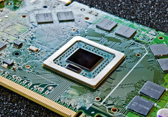
What is PCB Assembly ?
PCB Assembly manufacturer - Hitech Circuits Co., Limited
It’s the step in the manufacturing process in which you populate a blank board with the electronic components needed to make it into a functional printed circuit board. It’s these components that make a board into the circuit that enables an electronic product to function. PCB assembly typically takes place via one of two processes:
1. Surface-mount technology
SMT: SMT stands for “Surface Mount Technology“. The SMT components are very small sizes and comes in various packages like 0201, 0402, 0603, 1608 packages for resistors and capacitors. Similarly for Integrated circuits ICs we have SOIC, TSSOP, QFP and BGA.
The SMT components assembly is very difficult for human hands and can be time taking process so it is mostly done by automated pick and place machine.
2. Through-hole manufacturing
THT: THT stands for “Through hole Technology”. The components with leads and wires, like resistors, capacitors, inductors, PDIP ICs, transformers, transistors, IGBTs, MOSFETS are example.
The component has to be inserted on one side of PCB and pulled by leg on other side and cut the leg and solder it. The THT components assembly is usually done by hand soldering and is relatively easy.
Printed Circuit Board Assembly Techniques
There are only two common PCBA techniques available for use by a PCB designer. The methods are:
1. Automated PCB Assembly Techniques
Generally, this technique employs the use of state of the art machines, which are fully automatic. For example, the surface mount components are worth positioning with the aid of an automated pick and place machine.
Again, reflow soldering is commonly for surface mount components usually done in a reflow oven. An automated solder stencil is also used to apply the solder paste on the PCB.
Finally, high tech inspection machines are used to confirm and check the quality of the PCBA. Some of which include: Automated optical inspection machine (AOI), X-ray inspection machines, etc.
Above all, due to the precise monitoring, control of soldering, no human input and versatile machines.
This technique ensures utmost efficiency, output consistencies, and limits defects.
2. Manual PCB Assembly Techniques
This method is favorite for use with through-hole parts, which needs manual placement on the board. Besides, with these through-hole parts, it’s advisable you use wave soldering. Note that in the through- hole assembly process, you need to place the components and electronics on the PCB.
After that, you use wave soldering to solder the leads. Typically, you will need an individual to insert a component into a marked PTH. Once done, transfer the PCB to the next station where the next person will be on standby tasked with fixing another part.
What are the Benefits of SMT PCB Assembly?
SMT assembly provides many benefits and some of them are as follows:
It can be used to incorporate small components.
In SMT, the components can be placed on both sides of the board.
It assures high component densities.
Fewer holes need to be drilled for surface mounting than through-hole.
It require low initial costs and time for setting up the mass production.
SMT is the simpler and faster-automated assembly when compared to through-hole.
Errors regarding the component placement can be easily rectified.
Surface mount PCBs feature strong joints, which can easily withstand vibrations.
What are the techniques used in Surface Mount Technology?
There are several techniques for the reflow process. After applying the solder paste or a flux mixture on the board and after placing the components, the boards are conveyed to a reflow soldering oven. The techniques used for reflowing soldering include infrared lamps, hot gas convection, fluorocarbon liquids with a high boiling point, and so on.
What are the different testing methods used in SMT PCB Assembly?
Hitech Circuits as the PCB assembly manufacturer, we perform the following testing and inspection to ensure the quality of surface mount PCBs.
Automated Optical Inspection (AOI): This is performed before and after the soldering to identify the component placement, presence, and solder quality.
X-ray Testing: In this type of testing, the operator relies on the X-ray images of the PCB to check the solder joints and lead-less components such as Quad Flat Packs and ball grid arrays, which are generally not visible to naked eyes.
In-Circuit Testing (ICT): This method is used to detect manufacturing defects by testing the electrical properties in the SMT Assembly.
What type of files or documents should I send for SMT PCB Assembly?
Gerber Files: The file contains all details of physical board layers including solder masks, copper layers, drill data, legends, and so on.
Bill of Materials (BOM): This contains information on the list of items needed for the PCB manufacturing and the instructions of manufacturing.
Pick and Place File: This file contains information on all components to be used in the PCB design and their rotation and X-Y coordinates.
The whole process of PCB Assembly
1. Bare board loader machine
The first step in the PCB assembly is to arrange the bare boards on the rack, and the machine will automatically send the boards one by one into the SMT assembly line.
2. Printing solder paste
When PCB on the SMT production line, firstly, we have to print solder paste on it, and the solder paste will be printed on the pads of the PCB. These solder pastes will be melt and solder the electronic parts to the circuit board when it passes through the high-temperature reflow oven.
In addition, when testing new products, some people will use film board/adhesive cardboard instead of solder paste, which can increase the efficiency for adjusting the SMT machines.
3. Solder paste inspection machine(SPI)
Since the quality of solder paste printing is related to the quality of welding of subsequent parts, some SMT factories will use optical machine to check the quality of solder paste after printed the solder paste in order to ensure stable quality. If there any poorly printed solder paste board, we will wash off the solder paste on it and reprint, or remove the excess solder paste if there is redundant solder paste on it.
4. High speed SMT machine
Usually, we will put some small electronic parts (such as small resistors, capacitors, and inductors) to be printed on the circuit board first, and these parts will be slightly stuck by the solder paste just printed on the circuit board, so even if the speed of printing is very fast and the parts on the board will not fall away. But large parts are not suitable for use in such high speed SMT machines, which will slow down the speed of small parts assembly. And the parts will be shifted from the original position due to the rapid movement of the board.
5. Universal SMT machine
Universal SMT machine is also known as "slow machine", it will be assembled some large electronic components, such as BGA IC, connectors, etc., these parts need more accurate positions, so the alignment is very important. Use a camera to take a picture to confirm the position of the parts, so the speed is much slower than High speed SMT machine we taked before. Due to the size of the components here, not all of them are packed in tape and reel, and some may be packed in trays or tubes. But if you want the SMT machine to recognize the trays or tube-shaped packaging materials, you must configure an additional machine.
Generally, traditional SMT machines are using the principle of suction to move electronic parts, and in order to place the parts successfully, and there must be the flat surface on these electronic components for the suction nozzle of the SMT machine to absorb. However, for some electronic parts don’t have a flat surface for these machines, and it is necessary to order special nozzles for these special-shaped parts, or add a flat tape on the parts, or wear a flat cap for thees electronic parts.
6. Manual parts or visual inspection
After assembled all parts by the high speed SMT machine or Universal SMT machine and before going through the high-temperature reflow oven, and we will set up a visual inspection station here and to pick out the deviation parts or missing components boards etc., because we have to use a soldering iron to repair if there are still defectives boards after passing the high-temperature oven, which will affect the quality of the product and will also increase the cost. in addition, for some larger electronic parts or traditional DIP parts or some special reasons cannot be processed by the SMT machine before, they will be manually placed on pcb here.
7. Reflow oven
The purpose of reflow oven is to melt the solder paste and form a non-metallic compound on the component feet and the circuit board, that means to solder electronic components on the circuit board. The temperature rise and fall curves often affect the soldering quality of the entire circuit board. According to the characteristics of the solder materials, usually the reflow oven will set the preheating zone, soaking zone, reflow zone, and cooling zone to achieve the best soldering effect.
For example, the melting point for SAC305 solder paste with lead-free is about 217°C, which means that the temperature of the reflow oven must be higher than the melting points to remelt the solder paste. What's more, the maximum temperature in the reflow furnace should not exceed 250°C, otherwise many parts will be deformed or melted because they cannot withstand such a high temperature.
Basically, after the pcb passed through the reflow oven, the assembly for the entire circuit board is almost complete. If there are hand-soldered parts, we need to transfer to DIP process, and then we have to check the quality after reflow oven by QC department.
8. Automatic optical inspection(AOI)
The main purpose of setting up AOI is because some high density boards can’t be process the following ICT test, so we used AOI inspection to replace it. But even using AOI inspections, there still have the blind spots for such checking, for example, the solder pads under the components cannot be checked by AOI. At present, it can only check whether the parts have side standing issue, missing parts, displacement, polarity direction, solder bridges, lack of soldering etc., but cannot checking the BGA solderability, resistance value, capacitance value, inductance value and other components quality, so far AOI inspection can’t completely replace ICT test.
Therefore, there is still some risk if only AOI inspection is used to replace ICT testing, but ICT test is also not 100% make sure the good quality, we suggest these two ways can be combined with together to make sure the good quality.
9. PCB unloader machine
After the board is fully assembled, it will be retracted to the unloder machine, which has been designed to allow the SMT machine to automatically pick and place the board without damaging the quality for PCB.
10. Visual inspection for finished products
Normally there will be a visual inspection area in our SMT production line whether there is an AOI station or not, and it will help to check if there are any defectives after completed assembled the pcbs. If there is an AOI station, it can reduce the visual inspection worker on our SMT line, and to reduce the potential cost, and because it is still necessary to check some places that cannot be judged by AOI, many SMT factories will provide the mainly visual inspection templates at this station, which is convenient for visual inspection worker to inspect some key parts and polarity for components.
11. DIP process
DIP process is a very important process in the whole PCBA processing, and the processing quality will directly affect the functional for PCBA boards, so it is necessary to pay more attention to the DIP process. There are many preliminary preparations for DIP process. The basic process is to re-process the electronic components first, like to cut the extra pins for some DIP components, our staff received the components according to the BOM list, and will check whether the material part numbers and specifications are correct or not, and performs pre-production pre-processing according to the PCBA samples. The steps are: Use various related equipment (automatic capacitor pins cutting machine, jumper bending machine, diode and triode automatic forming machine, automatic belt forming machine and other machines) for processing.

12. ICT test
Printed Circuit board open/short circuit test (ICT, In-Circuit Test), The purpose of ICT test is mainly to test whether the components and circuits on the printed circuit board are open or short issues. It can also measure the basic characteristics of most components, such as resistance, capacitance, and inductance values to judge whether the functions of these parts are damaged, wrong parts or missing parts etc. after passing through the high-temperature reflow oven.
ICT test machines are divided into advanced and basic machines. The basic ICT test machines are generally called MDA (Manufacturing Defect Analyzer). It’s just to measure the basic characteristics of electronic components and judge open and short circuits issue we talked above.
In addition to all the functions of the basic ICT test machines, for advanced ICT test machine can also test the whole PCBA by using power, start to testing the PCBA boards by setting the program in the test machine. The advantage is that it can simulate the function of the printed circuit board under the actual power-on condition, this test can partly replace the following functional test machine (Function Test). But the cost for the test fixture of this advanced ICT test can probably buy a car, it’s too expensive and we suggest it can be used in mass production products.
13. PCBA function test
Functional testing is to make up for the ICT test, because ICT only tests the open and short circuits on the the PCBA board, and other functions such as BGA and other fuctions are not tested, so it is necessary to use a functional testing machine to test all functions on the whole PCBA board.
14. Cutting board (assembly board de-panel)
Normally, printed circuit boards will be produced in panel, and it will be assembled to increase the efficiency of SMT production. It means several single boards in one panel, such as two-in-one, four-in-one etc. After finished all the pcb assembly process, it needs to be cut into single boards, and for some printed circuit boards with only single boards also need to cut off some redundant board edges.
There are several ways to cut the printed circuit board. You can design the V-cut using the blade cutting machine (Scoring) or directly manually break off the board (not recommended). For more high density circuit boards, it will be used the professional splitting machine or the router to split the board without any damage the electronic components and printed circuit boards, but the cost and working hours will be a little longer.
Why Choose Hitech Circuits PCB Assembly Manufacturer for Your PCB Assembly Projects?
There are several PCB manufacturers specializing in PCB assemblyservices. However, Hitech Circuits PCB Assembly stands out owing to the following:
Assistance in Material Procurement:
Technically, in PCB assembly services, the quality of parts is the responsibility of the OEM; however, we ease your job by assisting you to make the right selection. We can help you procure all your parts of the same type own a single part number, thanks to our supply chain and vendor network as well as experience. This saves time and cost that goes in ordering single parts as you plan.
Testing procedures:
We are very focused on quality and thus implement stringent testing procedures at each stage of the assembly and after completion.
Fast Turnaround Times:
Our well-equipped facility and the right tools enable us to complete your requirements well before time, and without compromising on the quality or functioning of the PCBs. For simple designs we revert in 24 to 48 hours.
Cost Effectiveness:
While PCB assembly is a cost-effective alternative, we go a step further and assure that the parts you list are of a good quality and suitable for your requirement. Also, you can control the part flow and replenish them as needed. This eliminates the need to buy extra stock and store it.
Quick Quote:
We offer a quick quote based on your BOM. All you need is a detailed BOM, Gerber files, your application requirement sheet, and quantity.
We’re not one to stand still, which is why we use the latest equipment and the finest minds to create your PCB projects. We’re constantly keeping our finger on the pulse of the latest trends. And as a result, we know how to deliver the highest standards of PCB assembly to meet all your requirements.
Our dedicated, friendly customer service team also means that we support you every step of the way. Offering our expert guidance to ensure a complete PCB project that you’re happy with.
Contact us today
No matter what your printed circuit board assemblyneeds are, we always aim to deliver efficient, dependable solutions. For more information about our services, do not hesitate to get in touch with us today for a no-obligation quote
2 notes
·
View notes
Text
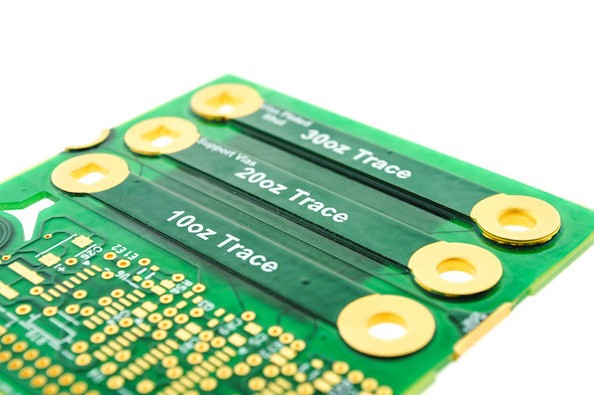
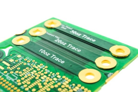
What is Heavy Copper PCB?
Heavy copper PCB is a circuit board with a copper thickness that is ≥ 3oz per sq. ft in its outer and inner layers. What makes a circuit board classified as a heavy copper PCB is its thicker plating. During the production of heavy copper PCB, copper thickness is enhanced through plated holes and sidewalls. For instance, when a PCB has 2 ounces of copper per sq. ft thickness, it is a standard PCB. However, if it has more than 3oz of copper, it is a heavy copper PCB. Heavy copper PCB is considered a reliable wiring option. Heavy copper PCB is different from extreme copper PCB which features within 20 oz to 200 oz per sq. ft.
What does Heavy Copper PCB offer?
Heavy copper PCB has a lot to offer. It has got some unique features that make it an ideal option for high-end applications. Let’s discuss some of the benefits of this PCB; Great thermal distribution: Due to its copper-plated vias, this PCB offers high thermal resistance. Heavy copper PCB are used in applications that demand high speed and high frequency. You can also use this PCB at harsh temperatures. Mechanical strength: Heavy copper PCB feature great mechanical strength. When this PCB is used, it makes the electrical system durable and robust. Good conductor: Heavy copper circuit boards are a good conductor. They are utilized in the production of electronics due to this feature. They help to link various boards together. These boards can transfer current.
How is Heavy Copper PCB Fabricated?
For the fabrication of heavy copper PCB, plating or etching is often used. The main aim is to add copper thickness to sidewalls and plated holes. The methods used in fabricating heavy copper PCB aren’t far-fetched. Heavy copper PCBs need special etching and plating methods to ensure the extra thickness of copper. Using the normal etching techniques for the fabrication of heavy copper PCBs isn’t ideal. Normal etching methods produce over-etched margins and edge lines that are uneven. PCB producers now use advanced etching and plating methods to achieve straight edges.
Heavy copper PCBs are produced via etching and plating methods. The major aim in the production of this PCB is to add copper thickness through sidewalls and plated-through holes. Heavy copper PCBs have several benefits which make them in high demand. Due to their outstanding features and benefits, they can meet your electrical requirements. These circuit boards will always dissipate heat generated due to heavy currents conduction. Electronics using heavy copper boards have been in use for a long time. Heavy copper can carry high currents. These boards will continue to meet the needs of various applications. High power circuit wirings can be developed using Heavy Copper PCBs. Such a wiring mechanism offers more reliable thermal stress handling and offers fine finishing while incorporating multiple channels on a single layer of a compact board.
Printed circuit boards (PCBs) are usually bonded with a layer of copper foil on a glass epoxy substrate. The thickness of the copper foil is usually 18μm, 35μm, 55μm, and 70μm. The most commonly used copper foil thickness is 35μm. Domestic copper foil thickness is generally 35 ~ 50μm, there are thinner than this such as 10μm, 18μm; And thicker than that like 70μm. The thickness of composite copper foil on 1~ 3mm thick substrate is about 35μm. The thickness of the composite copper foil on the substrate less than 1 mm thick is about 18μm, and the thickness of the cladding copper foil on the substrate thicker than 5mm is about 55μm. If the PCB copper foil thickness is 35μm, printed line width is 1mm, then every 10mm long, its resistance value is about 5mΩ, its inductance is about 4nH. When the di/dt of the digital integrated circuit chip on the PCB is 6mA/ns and the working current is 30mA, the noise voltage generated by each part of the circuit is estimated to be 0.15mV and 24mV according to the resistance value and inductance value of each 10mm printed line. Heavy Copper PCB boards can be made simply by combining two main processes: electroplating and etching. Compared to other PCBs, the circuit is made of a thin layer of copper foil. The copper plates are uniformly laminated with FR4 or other epoxy-based substances. The average weight of a Heavy Copper PCB can be 4 oz. (140μm), which is a better ratio than a copper-shared PCB. Let's look at the benefits.
Heavy Copper PCB Manufacturer & Circuit board Assembly – One-stop service Printed Circuit Boards (PCB) are usually coated with thick copper foil on a glass epoxy substrates commonly thickness of copper foil are 18μm, 35μm, 55μm, and 70μm. The most common copper foil is 35μm. The heavy copper PCB boards can simply be manufactured by two main processes plating and etching in the combine. As compared to other PCBs, the circuit is made of a thin layer of the Copper foil sheet. The plates of copper are laminated uniformly with FR4 or other epoxy-based substance. The average weight of the thick copper PCB weight could be 4oz (140μm), and this ratio is better as compared to another type of PCBs who have copper in common. Let’s check out the benefits of it.
Benefits of Heavy copper PCB Fabrication
Here are some of the advantages of heavy copper PCB, let’s follow them:
1. Favorable circumstances of Heavy Copper PCB
2. Plating innovation in overwhelming copper permitted a mix of plating and carving which causes in straight sidewalls and immaterial undercut.
3. The substantial copper plating creates high-current circuits and control circuits that watches the profoundly thick and straightforward whiskers’ structure.
4. This empowers the board fabricator to build the measure of copper thickness in plated gaps and by means of sidewalls.
5. The blend of substantial copper results on a solitary board called PowerLink.
6. The substantial copper in the PCB likewise encourages in associating with the standard circuits.
7. This lessens layer tally, low impedance control conveyance, littler impressions, and potential cost investment funds.
8. For development purposes, it expands the continuance to warm strains.
9. It has expanded the current conveying limit.
10. Overwhelming copper plating brings higher current through the board and moves the warmth to the outside heat sink
1 note
·
View note
Text
What is Ceramic PCB?
Ceramic PCB board is also called ceramic substrate, ceramic circuit board, ceramic copper coated plate, ceramic substrate refers to the copper foil directly bonded to alumina (Al2O3) or aluminum nitride (AlN) ceramic substrate or other ceramic substrate surface (single or double) on the special process board.
The ceramic pcb can be described as an organic binder and ceramic powder that conducts heat. The thermal conductivity at which this PCB is prepared is between 9 to 20W/m.
To explain further, ceramic PCBs are printed circuit boards, with ceramic as its base material. This base material is highly thermally conductive like aluminum nitride, alumina, and beryllium oxide. These are very effective in the transfer of heat from hot spots and then dissipating this heat over the entire surface.
Asides from this, the fabrication of ceramic PCB is done with the LAM technology. This technology is a laser quick activation metallization type. Therefore, ceramic PCBs are highly versatile and can easily substitute the whole traditional PCBs. This PCB will achieve this with even more enhanced performance and involving less complicated construction.
1. The difference between ceramic substrate and pcb board
Ceramic substrate is that we say ceramic circuit board, ceramic pcb and printed circuit board have the same circuit interconnection, through hole conduction characteristics. So what are the differences between ceramic substrate and pcb board?
(1)The thermal conductivity of PCB board and ceramic substrate is different
Ceramic substrate is made of ceramic substrate, that is, the medium is ceramic material, including alumina ceramic base, aluminum nitride ceramic base, silicon nitride ceramic base, ceramic heat dissipation performance is very good, the thermal conductivity of ceramic substrate from 25w to 230w, different ceramic medium thermal conductivity is different. The thermal conductivity of alumina ceramic substrate is 25w~30w, the thermal conductivity of aluminum nitride ceramic substrate is above 170w, and the thermal conductivity of silicon nitride ceramic substrate is 80w~90w. Then pcb board is usually the use of medium is fr4 or metal substrate, thermal conductivity is less than 3w, and the gap is too large compared with ceramic substrate, especially the need for high heat dissipation performance of the product field, ceramic substrate has become a very popular medium material.
2. Ceramic substrate and pcb board insulation is different
Ceramic substrate is generally line layer - ceramic base - line layer structure, ceramic substrate insulation is very good, is also determined by the ceramic material itself, no need to add insulation layer. pcb board needs to add an insulating layer to play a mobile insulation role, but the insulation effect is far less than ceramic substrate.
(3)The heat dissipation structure of ceramic substrate is different from that of pcb board
The heat dissipation structure of the ceramic substrate is the structure of the circuit layer - ceramic base - circuit board layer. Because there is no insulating layer in the middle, the heat of the device is transferred directly from the ceramic base to the circuit layer and the heat dissipation is out, the heat dissipation is fast and the effect is good. pcb board is the need for heat from the medium layer - insulation layer - line layer, separated by an insulation layer at the same time, the dielectric layer itself of the thermal conductivity is poor, then add heat conduction adhesive, heat conduction effect is still not improved, often can not achieve the purpose of rapid heat dissipation device. In particular, some high-power devices need to use ceramic substrate as a cooling substrate in the product field where the heat dissipation and temperature change is relatively large.
(4)Ceramic substrate and pcb board application is different
Ceramic substrate and pcb board application is different, mainly the performance of the two is different, ceramic substrate is used in high thermal conductivity, high heat dissipation, high insulation, product field, such as high power LED lighting, high power module, high-frequency communication, track power supply; Ordinary pcb board is used in some more extensive, heat dissipation, insulation and other requirements are not strict, used in private commercial commodities.
(5) The price of ceramic substrate is different from that of pcb board
The material and performance of ceramic substrate and pcb board are different, and the final decision is that their prices are different. The board of ceramic substrate is very high and the production cost is high.
Ceramic substrate has outstanding advantages, but the ceramic substrate is fragile and has a high scrap rate, which requires a high level of production technology. However, you can't make a circuit board with the size of more than one meter like ordinary pcb boards. Hitech Circuits has more than 10 years of experience in the ceramic circuit board industry, and many universities and R & D institutions are in cooperation, welcome to inquiry.
2.Ceramic substrate and high-frequency plate difference
The material is different. The ceramic substrate is made of aluminum oxide or aluminum nitride, and the high frequency plate is made of Rogers, Yaron, PTFE, etc., with low dielectric constant and high frequency communication speed.
Performance is different. Ceramic substrate is widely used in refrigeration and systems, high power modules, automotive electronics and other fields. High frequency board is mainly used in high frequency communication field, aviation, high-end consumer electronics and so on. High-frequency communication field involves heat dissipation requirements, usually need to be combined with the ceramic base and high frequency plate, such as high frequency ceramic pcb.
1. Application of ceramic substrate
Ceramic substrates are used in led chips to achieve better thermal conductivity. In addition, ceramic substrate is also used to make ceramic chips in the following electronic devices:
◆High power semiconductor module
◆Semiconductor cooler, electronic heater; Power control circuit, power mixing circuit
◆Intelligent power module; High frequency switching power supply, solid state relay
◆Automotive electronics, aerospace and military electronics components
◆Solar panel module; Telecommunications private exchange, receiving system; Laser and other industrial electronics
Application of ceramic substrate in third generation semiconductor
The mainstream power devices represented by MOSFET, IGBT and transistor occupy a place in their own frequency and power supply segments. Due to the comprehensive excellent performance of IGBT, it has replaced GTR, become the inverter, UPS, frequency converter, motor drive, high-power switching power supply, especially now the hot electric vehicle, high-speed rail and other power electronic devices in the mainstream devices.
Application of alumina ceramic substrate in electronic power field
In the field of power electronics, such as power switching power supply, electric drive, etc., dielectric ceramic substrate is needed to achieve better thermal conductivity, prevent current burn out and short circuit.
Application of alumina ceramic co-fired plate in lithium battery industry
With the recommendation of artificial intelligence and environmental protection, the automobile industry has also launched electric cars, mainly through battery storage. Lithium batteries made of ceramic substrate can achieve better current and heat dissipation functions, promoting the market demand for new energy vehicles.
2. Advantages of ceramic substrate
A. The thermal expansion coefficient of ceramic substrate is close to that of silicon chip, which can save Mo sheet of transition layer, save labor, save material and reduce cost;
B. Reduce the welding layer, reduce the thermal resistance, reduce the cavity;
C. Under the same load flow, the wire width of copper foil 0.3mm thick is only 10% of that of ordinary printed circuit board;
D. Excellent thermal conductivity, so that the chip packaging is very compact, so that the power density is greatly increased, improve the reliability of the system and device;
E. Ultra-thin (0.25mm) ceramic substrate can replace BeO, without environmental toxicity problems;
F. Large load capacity, 100A current continuously through 1mm wide 0.3mm thick copper body, temperature rise about 17℃; With 100A current continuously passing through a 2mm wide 0.3mm thick copper body, the temperature rise is only about 5℃.
G. Low thermal resistance, 10×10mm ceramic substrate 'thermal resistance of 0.63mm thickness of ceramic substrate is 0.31K/W, 0.38mm thickness of ceramic substrate is 0.19K/W, 0.25mm thickness of ceramic substrate is 0.14K/W.
H. High insulation and high pressure resistance to ensure personal safety and equipment protection.
I. New packaging and assembly methods can be realized, so that the product is highly integrated and the size is reduced.
3. Ceramic substrate technology
At present, the common types of ceramic heat dissipation substrate include HTCC, LTCC, DBC and DPC. DBC and DPC for the domestic in recent years to develop mature, and energy production of professional technology, DBC is the use of high temperature heating Al2O3 and Cu plate combination, its technical bottleneck is not easy to solve the problem of micro-pores between Al2O3 and Cu plate, which makes the mass production energy and yield of the product by the greater challenge. DPC technology is the use of direct copper plating technology, Cu deposition on the Al2O3 substrate, its process combined with the material and film technology, its product is the most commonly used ceramic cooling substrate in recent years. However, its material control and process technology integration ability requirements are high, which makes the technical threshold of entering the DPC industry and stable production is relatively high.
(1) HTCC (High-Temperature Co-fired Ceramic)
The manufacturing process of HTCC is very similar to that of LTCC. The main difference is that the ceramic powder of HTCC is not added with glass material. Therefore, the ceramic powder of HTCC must be dried and hardened into embryonic form at a high temperature of 1300~1600℃. Due to its high co-firing temperature, the choice of metal conductor materials is limited, its main materials for high melting point but poor conductivity tungsten, molybdenum, manganese... Such as metal, and finally laminated sintering molding.
(2) LTCC (Low-Temperature Co-fired Ceramic)
LTCC is also known as low-temperature co-fired multilayer ceramic substrate. In this technology, inorganic aluminum oxide powder and about 30%~50% glass material are combined with organic binder to make it evenly mixed into mud slurry. Then, the slurry is scraped into sheets with a scraper, and then through a drying process, the sheet slurry is formed into a thin piece of raw blank. As the transmission of signals at all levels
For the internal lines of LTCC, the screen printing technology is used to fill holes and print lines on the raw embryos, and the internal and external electrodes can be used respectively of silver, copper, gold and other metals. Finally, the layers are stacked and sintered in the sintering furnace at 850~900℃.
(3) Direct Bonded Copper (DBC)
Direct copper coating technology is the use of copper oxygen eutectic liquid directly on the ceramic coating, the basic principle is to introduce an appropriate amount of oxygen between copper and ceramic before or during the coating process, in the range of 1065℃~1083℃, copper and oxygen form Cu-O eutectic liquid, DBC technology uses the eutectic solution to chemically react with the ceramic substrate to form CuAlO2 or CuAl2O4 phase on the one hand, and to infiltrate the copper foil to realize the combination of the ceramic substrate and copper plate on the other hand.
(4) DPC (Direct Plate Copper)
DPC is also known as direct copper-plated substrate. Take DPC substrate process as an example: First of all, the ceramic substrate is pre-treated and cleaned, and the ceramic substrate is sputtered on the ceramic substrate and combined with the copper composite layer by using the vacuum coating technology of thin film manufacturing. Then the circuit is made by the re-exposure, development, etching and film removal process with the yellow light microshadow photoresistance. Finally, the thickness of the circuit is increased by electroplating/electroless plating deposition, and the metallized circuit is made after the photoresistance is removed.
3. Production process of ceramic substrate
1. Drilling
Ceramic substrate is generally used by laser punching, compared with the traditional punching technology, laser punching technology has the advantages of high precision, fast speed, high efficiency, large-scale mass punching, suitable for the vast majority of hard and soft materials, no loss to tools, in line with the printed circuit board high density interconnection, fine development.
Through the laser drilling process of ceramic substrate has high bonding force of ceramic and metal, no falling off, foaming phenomenon, to achieve the effect of growth together, high surface smoothness, roughness in 0.1μm ~ 0.3μm, laser drilling aperture in 0.15mm-0.5mm, even can reach 0.06mm.
2、Copper-clad
Copper coating refers to the area without wiring on the circuit board covered with copper foil, connected with the ground wire, in order to increase the ground wire area, reduce the loop area, reduce voltage drop, improve power efficiency and anti-interference ability. Copper coating can not only reduce the ground impedance, but also reduce the cross-sectional area of the loop and enhance the mirror loop of the signal. Therefore, the copper coating process plays a very key role in the ceramic substrate PCB process, incomplete, truncated mirror loop or incorrect position of the copper layer often lead to new interference, have a negative impact on the use of the board.
3. Etching
Ceramic substrates also need to be etched, with the circuit pattern pre-coated with a lead-tin resist layer, and then chemically etched away the unprotected, non-conductive copper to form the circuit. Etching is divided into inner layer etching and outer layer etching, inner layer etching using acid etching, with wet film or dry film as corrosion resistance; The outer etching is alkaline etching with tin and lead as resist.
There are many kinds of manufacturing process of ceramic products in circuit board factory. It is said that there are more than 30 kinds of manufacturing processes, such as dry pressing, grouting, extrusion, injection, casting and isostatic pressing. Because the electronic ceramic substrate is a "flat" type, the shape is not complicated, the manufacturing process of dry forming and processing is simple and the cost is low, so most of them use dry pressing forming method. The manufacturing process of dry press PCB electronic ceramics mainly includes blank forming, blank sintering and finishing, forming circuit on the substrate.
1. Green manufacturing of ceramic substrate (forming)
Use high purity alumina (content ≥95% Al2O3) powder (different particle sizes are required depending on the purpose and manufacturing method. For example, from a few illiterates to tens of microns) and additives (mainly adhesives, dispersants, etc.). Form a "paste" or processed material.
(1) Dry pressing of ceramic substrate to produce green parts (or "green").
Dry pressing billet is the use of high purity alumina (electronic ceramics with alumina content greater than 92%, most of the use of 99%) powder (dry pressing particles shall not exceed 60μm, for extrusion, rolling, injection and other powder particles should be controlled within 1μm) add the appropriate amount of plasticizer and binder, mixed evenly after dry pressing billet. At present, the offspring of square or round pieces can reach 0.50mm, or even ≤0.3mm (depending on plate size). Dry pressed billets can be processed before sintering, such as dimensioning and drilling. Machining, but be careful to compensate for the size shrinkage caused by sintering (magnify the size of the shrinkage).
(2) Production of green billet by ceramic substrate spreading method.
Flow glue liquid (aluminum oxide powder + solvent + dispersant + adhesive + plasticizer mixed evenly + screening) manufacturing + flow casting (in the flow casting machine glue on metal or heat-resistant polyester belt) + drying + trimming (can also be other processing) + degreasing + sintering and other processes. It can realize automation and scale production.
2. Sintering and finishing of green billet after sintering. The raw parts of ceramic substrate often need to be "sintered" and finished after sintering.
(1) Sintering of raw ceramic substrate.
Ceramic billet "sintering" refers to the process of "sintering", the billet (volume) in the cavity, air, impurities and organic matter such as dry pressure removal, so that its volatilization, combustion, extrusion, and removal of alumina particles. Achieve close contact or combined growth process, so after sintering of ceramic green billet, there will be weight loss, size shrinkage, shape deformation, compressive strength increase and porosity reduction and other changes.
The sintering methods of ceramic billet are as follows: ① atmospheric sintering, non-pressure sintering will bring large deformation; ② pressure (hot pressing) sintering, pressure sintering, can get good flat products is the most commonly used method; ③ Hot isostatic sintering is the use of high pressure hot gas sintering. Its characteristic products are finished at the same temperature and pressure. All kinds of performance balance, the cost is relatively high. In the added value of products, or aerospace, national defense and military products in the use of this sintering method, such as the military field of mirrors, nuclear fuel, barrel and other products. The sintering temperature of dry pressed alumina green billets is mostly between 1200℃ and 1600℃ (depending on composition and flux).
(2) Finishing of ceramic substrate after sintering (cooked) blank.
Most sintered ceramic billets require finishing. The purpose is: ① to obtain a flat surface. In the process of high temperature sintering of green billet, due to the imbalance of particle distribution, voids, impurities and organic matter in the green billet, it will cause deformation, unevenness or excessive roughness and difference. These defects can be solved by surface finishing; ② Obtain high finish surface, such as specular reflection, or improve lubricity (wear resistance).
Surface polishing treatment is to use polishing materials (such as silicon carbide, B4C) or diamond sand paste to gradually polish the surface from coarse to fine abrasive. Generally speaking, the use of AlO powder or diamond paste ≤1μm, or laser or ultrasonic processing to achieve.
(3) strong (steel) treatment.
After surface polishing, in order to improve the mechanical strength (such as bending strength, etc.), electronic ray vacuum coating, sputtering vacuum coating, chemical vapor evaporation and other methods can be used to plating a layer of silicon compound film, through 1200℃ ~ 1600℃ heat treatment, can significantly improve the mechanical strength of ceramic parts!
3. Form a conductive pattern (circuit) on the substrate
To process conductive graphics (circuits) on ceramic substrates, it is necessary to manufacture copper-coated ceramic substrates first, and then to manufacture ceramic printed circuit boards according to PCB technology.
(1) Forming a copper-covered ceramic substrate. There are currently two methods of forming copper-coated ceramic substrates.
① Laminating method. It is formed by hot pressing one side of oxidized copper foil and alumina ceramic substrate. That is, the ceramic surface is treated (such as laser, plasma, etc.), get activated or rough surface, and then according to the "copper foil + heat-resistant binder layer + ceramic + heat-resistant binder layer + copper foil" laminate together, after 1020℃ ~ 1060℃ sintering, the formation of double-sided copper coated ceramic laminate. ② Electroplating method. After plasma treatment, the ceramic substrate is "sputtered titanium film + sputtered nickel film + sputtered copper film", and then conventional electroplating copper to the required copper thickness, that is, the formation of double-sided copper-coated ceramic substrate.
(2) Single and double sided ceramic PCB board manufacturing. According to traditional PCB manufacturing techniques, single - and double-sided copper-coated ceramic substrates are used.
(3) ceramic multilayer plate manufacturing.
① In single and double panels repeatedly coated insulation layer (alumina), sintering, wiring, sintering to form PCB multilayer board, or the use of casting manufacturing technology to complete. ② Ceramic multilayer plate is manufactured by casting method. The raw tape is formed on the casting machine, then drilling, plugging (conductive glue, etc.), printing (conductive circuit, etc.), cutting, laminating, isostatic pressing to form ceramic multilayer plate. Hitech Circuits has more than 10 years of experience in manufacturing ceramic substrates, so feel free to consult them if you need to know more technical questions.
1 note
·
View note
Text
One-stop PCB assembly service and PCB manufacturing supplier -- Hitechpcba
As a leading one-stop electronics manufacturing services provider in China, Hitech Circuits Co., Limited offers high quality, cost effective and quick turn PCB board products, Printed Circuit board, PCB assembly, electronics assembly manufacturing, Electronic parts components sourcing services for your new products development.
With mature supply chain, talented design team, advanced manufacturing techniques and quality control systems, Hitech Circuits Co., Limited is able to provide one-stop electronics manufacturing services and solution for our customers to help them stand out in the marketplace.
4 notes
·
View notes
Text
PCB Assembly manufacturer--Hitechpcba
Hitechpcba is a wоrld-lеаding PCB Manufacturing & PCB Assembly company with more than 20 years experience in the electronics manufacturing industry. We focus on PCB Design, PCB Layout, Circuit board fabrication, Turnkey PCB assembly, and electronic parts sourcing services.
With mature supply chain, talented design team, advanced manufacturing techniques and quality control systems, Hitechpcba is able to provide one-stop electronics manufacturing services and solution for our customers to help them stand out in the marketplace.

5 notes
·
View notes