
Orbit & Skyline is a trusted semiconductor partner that provides turnkey solutions in the semiconductor domain. Our team has global fab experience in equipment engineering, process engineering, and facility management. We offer semiconductor OEMs and device manufacturers the most comprehensive and synergistic solution. As a fast-growing semiconductor services company with a global footprint, we service most fabs worldwide. Our intense customer focus is geared towards meeting and exceeding expectations.
Don't wanna be here? Send us removal request.
Statistics
We looked inside some of the posts by orbitandskyline and here's what we found interesting.
Average Info
Notes Per Post
1
Likes Per Post
1
Reblog Per Post
0
Reply Per Post
0
Time Between Posts
5 days
Number of Posts By Type
Text
11
Last Seen Tumblr Blogs


Fun Fact
1,644 Tumblr posts in 1 second.
Text
From Smartphones to Satellites: The Rise of Compound Semiconductors

In today’s rapidly advancing electronics landscape, semiconductors form the foundation of nearly every modern innovation—from everyday smartphones to cutting-edge satellites and electric vehicles. While silicon has long been the cornerstone of the semiconductor industry, a new class of materials—compound semiconductors—is stepping into the spotlight, offering unique advantages for high-performance and next-generation applications.
This blog explores the world of compound semiconductors: their types, unique properties, applications, challenges, and their immense potential to shape future technologies.
At Orbit & Skyline, we’re helping to accelerate the adoption of compound semiconductors through our specialized Semiconductor FAB Solutions and Semiconductor Material Supply expertise.
What Are Compound Semiconductors?
Unlike elemental semiconductors such as silicon (Si) and germanium (Ge), compound semiconductors are made by combining two or more elements, typically from groups III, V, II, and VI of the periodic table. This combination unlocks specialized electrical, optical, and thermal properties that pure elements cannot achieve.
Some common examples include:
Gallium Arsenide (GaAs)
Indium Phosphide (InP)
Gallium Nitride (GaN)
Silicon Carbide (SiC)
These materials are categorized based on the groups of their constituent elements:
III-V Compounds (e.g., GaAs, InP, GaN)
II-VI Compounds (e.g., CdTe, ZnSe)
IV-IV Compounds (e.g., SiC)
Types of Compound Semiconductors
Compound semiconductors can be further classified into:
III-V Compounds: Known for their excellent electrical properties and direct band gaps, these materials are widely used in high-frequency electronics and optoelectronics.
II-VI Compounds: Efficient in light absorption and emission, they are often used in solar cells and LEDs.
IV-IV Compounds: SiC stands out for its wide band gap and outstanding thermal conductivity, making it ideal for power electronics.
Ternary and Quaternary Compounds: Materials like Aluminum Gallium Arsenide (AlGaAs) and Indium Gallium Nitride (InGaN) allow engineers to "tune" material properties such as band gaps and lattice constants, thanks to advanced Process Engineering techniques.
Key Properties of Compound Semiconductors
Compound semiconductors bring several key advantages over silicon:
High Electron Mobility: Materials like GaAs enable faster electron movement, supporting high-frequency, high-speed devices.
Wide Band Gaps: Materials such as GaN and SiC can handle higher voltages and temperatures—critical for power and harsh-environment applications.
Direct Band Gaps: Unlike silicon, many compound semiconductors efficiently emit and absorb light, making them ideal for optoelectronics.
High Saturation Velocity: Essential for high-frequency and high-speed applications.
Radiation Resistance: Higher tolerance to radiation makes them suitable for space exploration and nuclear environments.
Superior Thermal Conductivity: Especially in SiC, enabling efficient heat dissipation.
Applications of Compound Semiconductors
Due to their exceptional properties, compound semiconductors are vital in a broad range of industries:
Optoelectronics: GaN-based LEDs, laser diodes, and CdTe solar cells.
High-Frequency Electronics: Key components in 5G infrastructure, satellite communications, radar, and microwave systems.
Power Electronics: GaN and SiC power devices revolutionize electric vehicles, renewable energy systems, and efficient power supplies.
RF and Microwave Devices: Critical for wireless communications and defense systems.
Sensors and Detectors: Deployed in medical imaging, environmental monitoring, and industrial sensing.
Challenges and the Road Ahead
Despite their advantages, compound semiconductors come with challenges:
Higher Production Costs: Crystal growth and processing for compound materials remain more expensive than traditional silicon.
Manufacturing Complexity: Precise control overgrowth processes are essential to minimize defects. Orbit & Skyline supports this precision with Equipment Engineering, Process Engineering, and Tool Hook-Up Services.
Scalability Issues: Meeting the growing demand while maintaining high quality remains a challenge.
However, innovation is rapidly overcoming these barriers. Techniques like Molecular Beam Epitaxy (MBE) and Metal-Organic Chemical Vapor Deposition (MOCVD) are enhancing crystal quality while driving down production costs.
The demand for energy-efficient electronics, 5G connectivity, EVs, and renewable energy solutions is fueling heavy investment into compound semiconductor research—positioning them as a cornerstone of future technological advancements.
Conclusion
Compound semiconductors are no longer just a niche innovation—they are transforming industries and enabling the technologies of tomorrow. Their superior electron mobility, wide band gaps, and direct optical transitions are unlocking capabilities that silicon alone cannot achieve.
At Orbit & Skyline, we are proud to be at the forefront of this revolution. Through our integrated Semiconductor FAB Solutions, Global Field Engineering Services, and Material Supply Expertise, we enable faster, scalable, and more efficient compound semiconductor adoption.
With 15+ years of industry leadership and a global network of 500+ skilled engineers, Orbit & Skyline is your trusted partner for semiconductor innovation.
Ready to take the next step? Connect with us at [email protected] to learn more about how we can power your next breakthrough.
#OrbitAndSkyline#SemiconductorSolutions#FABSolutions#MaterialSupply#EngineeringExcellence#ProcessEngineering#ToolHookUpServices
0 notes
Text
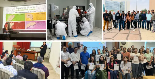
Empowering Employees Through Training & Development at Orbit & Skyline

"Tell me and I forget. Teach me and I may remember. Involve me and I learn." – Benjamin Franklin
At Orbit & Skyline, learning is more than just acquiring knowledge—it’s an immersive experience that fuels growth, innovation, and collaboration. Throughout 2024, we reimagined our approach to employee training, turning it into an engaging journey packed with real-life insights, interactive formats, and measurable impact.
Beyond Conventional Training
Gone are the days of generic, one-size-fits-all training programs. Our sessions are tailor-made for each audience, ensuring relevance and connection. With case studies, role-playing, and peer-driven discussions, employees don’t just absorb knowledge—they contribute to it. Each training becomes a collaborative effort where everyone learns and grows together.
Embedding 21st Century Skills
No matter the topic, every training module at Orbit & Skyline integrates the 4Cs essential for future-ready professionals:
Creativity – Inspiring out-of-the-box thinking and inventive solutions.
Critical Thinking – Strengthening analytical and decision-making skills.
Communication – Enhancing confidence and clarity in everyday interactions.
Collaboration – Promoting synergy across departments to drive results.
Our approach is paying off—94% of our employees participated in at least one training in 2024, with an outstanding 96% satisfaction rate.
The Three Pillars of Our Training Ecosystem
Technical Training Led by internal experts and external professionals, these sessions hone role-specific skills aligned with key performance indicators (KPIs).
Non-Technical Training Covering topics like Artificial Intelligence, Microsoft Tools, Soft Skills, Safety, and Holistic Well-being, these sessions ensure our teams stay agile and future ready.
Leadership Development From management offsites to leadership bootcamps, we prepare tomorrow’s leaders through hands-on experiences and targeted interventions.
Orbit Academy: Where Learning Comes Alive Our In-house Learning Management System, Orbit Academy, ensures a smooth and enriching training experience. With gamified modules, interactive content, and rewards, learning becomes both fun and impactful. We also collaborate with leading institutions like IIT, IIM, KPMG, Mitsubishi, and SMC to bring world-class training to our employees.
What’s Ahead in 2025?
Productivity Training: A 12-month program introducing 12 cutting-edge tools to help teams “work smarter, not just harder.”
SHIFT Program (Scout, Hire, Integrate, Forge & Transform): A practical cleanroom training initiative designed for engineers stepping into the semiconductor space.
GFO Elevate: A high impact bootcamp crafted to sharpen skills of our Global Field Operations Engineers.
Building a Future-Ready Workforce
At Orbit & Skyline, training is more than an HR initiative—it’s a strategic investment in our people. By prioritizing continuous learning, we empower our workforce to stay ahead of industry trends and become leaders of change.
We’re not just preparing for the future—we’re creating it, one training session at a time.
#EmployeeEmpowerment#LearningCulture#LearningAndDevelopment#CorporateTraining#SkillBuilding#LeadershipDevelopment#OrbitAndSkyline
0 notes
Text
Building a Global Team: Orbit & Skyline’s Approach to Diversity and Inclusion

In today’s interconnected world, an organization’s strength lies in how well it brings together diverse talents, ideas, and perspectives. At Orbit & Skyline, we believe diversity and inclusion are not just ethical imperatives—they’re strategic assets that power innovation, enrich employee experience, and support long-term success.
Our culture is grounded in the values of honesty, integrity, teamwork, and open communication. These aren’t simply guiding principles; they’re part of our everyday behaviour. With these values at the core, we’ve created a workplace where diversity, equity, and inclusion (DEI) are deeply embedded in our operations—evident in our exceptional employee satisfaction, with over 92% of team members expressing pride in their work.
What Diversity, Equity & Inclusion Mean to Us
Before highlighting our initiatives, it’s important to define what DEI stands for in our workplace:
Diversity: The representation of different identities across our workforce—such as race, gender, ethnicity, age, ability, sexual orientation, and cultural background.
Equity: Ensuring fair treatment, access, and opportunities while working to eliminate barriers that create disparities.
Inclusion: Building an environment where every individual feels respected, supported, and valued—empowering all voices to be heard and appreciated.
Inclusive Leadership Starts at the Top
At Orbit & Skyline, inclusive leadership is a top priority. We are committed to promoting talent from diverse backgrounds into leadership roles. Representation at decision-making levels not only inspires future leaders but also ensures our strategies reflect a wide range of perspectives.
Recruitment with a DEI Focus
We’ve developed thoughtful recruitment strategies that eliminate bias and promote equal opportunity:
Structured Interviews & Evaluation: Candidates are evaluated using standardized processes that focus on merit and skill.
Bias Training for Hiring Managers: Ongoing training helps managers recognize and reduce unconscious bias during the hiring process, ensuring fair and inclusive practices.
Empowering Employees Through Growth
We believe that growth is most impactful when it’s continuous and personalized:
Customized Learning Paths: We support individual career goals through personalized learning journeys.
Technical Training & Certifications: Ongoing technical programs keep our teams ahead of industry trends and help them pursue recognized certifications.
Mentorship Programs: New and mid-career professionals are paired with experienced mentors to guide their development and strengthen their sense of belonging.
Supporting Well-being & Work-Life Balance
A truly inclusive organization supports the whole person—both at and beyond the workplace:
On-site Creche Facility: We support working parents by offering convenient childcare solutions.
Annual Health Checkups: Proactive wellness programs help our team stay healthy and stress-free.
Feedback Channels: We actively listen through regular pulse surveys and employee feedback loops, turning insights into improvements.
Creating a Vibrant, Inclusive Culture
We celebrate what makes us unique—and what brings us together:
Festival Celebrations: We honor the diverse cultural roots of our team by celebrating festivals that reflect our shared humanity and heritage.
Engineers Day: An opportunity for cross-departmental collaboration, where teams build working models and showcase creativity while strengthening interdepartmental bonds.
Team Engagement Activities: From quarterly lunches to annual celebrations, we create spaces for connection and celebration.
Fun Fridays & Special Events: Informal gatherings that spark creativity, joy, and camaraderie.
Buddy Program: New employees are welcomed through a buddy system that eases their onboarding and builds early connections within the team.
Our Commitment to a Diverse Future
At Orbit & Skyline, building an inclusive team is a continuous journey—one that requires conscious effort and commitment at every level. Through inclusive leadership, equitable hiring, employee development, and a vibrant cultural environment, we’re shaping a workplace where every individual can thrive.
We invite individuals from all backgrounds to join us in building the future of the semiconductor industry. When everyone has a seat at the table, innovation isn’t just possible—it thrives.
Looking for a reliable semiconductor solutions partner? Reach out to us at [email protected]
0 notes
Text
What is the future of compound semiconductors, and how is India positioning itself in this space?
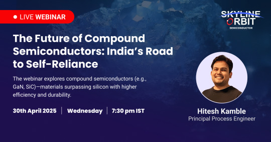
If you’re curious about the next big leap in semiconductor technology compound semiconductors and India’s growing role in this transformation, there’s an exciting live webinar you shouldn’t miss!
Webinar: The Future of Compound Semiconductors: India’s Road to Self-Reliance 📅 Date: 30 April 🕒 Time: 7:30 PM IST 🖥️ Where: Online (Live on Microsoft Teams) 🔗 Join Here: Click to Attend
What You’ll Learn:
Why compound semiconductors (like GaN, SiC) are replacing silicon—and what that means for the industry.
Technical differences between traditional silicon and compound semiconductors (bandgap, electron mobility, etc.).
Real-world applications across 5G, electric vehicles, defense, and renewable energy.
Global market outlook—projected to hit $150B by 2030—and the supply chain hurdles that come with it.
India’s emerging ecosystem—from talent and research to fab infrastructure and innovations like GaN LEDs and SiC wafers.
About the Speaker:
Hitesh Kamble, Principal Process Engineer at Orbit & Skyline Semiconductor Services, brings over 10 years of hands-on experience in III-V and compound semiconductor fabrication. Starting his journey at IIT Bombay, he now leads process development at Orbit & Skyline, having successfully led III-V fab startups and device tape-outs focused on GaN/GaAs technologies.
Don’t miss this opportunity to learn from an industry expert and ask your questions live!
Whether you're an engineer, a semiconductor enthusiast, or exploring careers in deep tech—this webinar is packed with insights that matter.
Register now and be part of the conversation shaping India's semiconductor future!
0 notes
Text
Legacy Tool Management: Prolonging the Lifespan of Semiconductor Equipment

In an industry driven by rapid innovation, legacy semiconductor tools continue to hold vital importance—especially in manufacturing processes based on mature nodes such as 180nm to 45nm. These nodes are indispensable for producing reliable, cost-efficient chips used in consumer electronics, automotive systems, and IoT devices. Rather than being phased out, legacy tools are being recognized as strategic assets in sustaining global semiconductor supply chains.
The Market for Mature Nodes: A Growing Opportunity
The demand for legacy node technologies remains strong, with the market size surpassing $50 billion. Industrial, automotive, and smart device sectors heavily rely on these nodes due to their affordability and proven reliability. As a result, manufacturers are prioritizing efforts to maximize the performance and longevity of legacy equipment to meet this ongoing demand.
Why Extend the Life of Legacy Tools?
Extending the lifespan of existing semiconductor tools offers numerous advantages:
Cost Savings Revitalizing current tools eliminates the need for hefty investments in new equipment.
Operational Continuity Ensures uninterrupted production of high-demand, mature-node products.
Sustainability Reduces electronic waste and supports eco-friendly manufacturing by lengthening equipment lifecycles.
Navigating the Challenges of Legacy Equipment
One of the core obstacles in legacy tool management is sourcing spare parts—particularly electronic components that typically have a lifecycle of just five years. As OEMs shift focus to advanced technologies, replacement parts for aging tools become increasingly scarce.
To maintain uptime and production efficiency, fabs must implement a proactive strategy involving detailed supply chain oversight, ongoing vendor collaboration, and strategic inventory management. A failure in this area can result in significant production delays and financial losses.
Orbit & Skyline: Leading the Charge in Legacy Tool Support
Recognizing the critical need for legacy tool solutions, Orbit & Skyline has invested heavily in supporting fabs worldwide through its dedicated Center of Excellence—a cutting-edge facility tailored to legacy tool challenges.
What Sets Orbit & Skyline Apart?
With more than 15 years of industry experience and a global team of over 500 engineers, Orbit & Skyline delivers comprehensive, end-to-end support for legacy equipment. The company’s strengths include:
Managing over 3,000 tools globally across etch, deposition, and clean processes
Securing spare part continuity via strong OEM and third-party relationships
Designing innovative, customized solutions for legacy systems
Developing resilient supply chain strategies to counter obsolescence
Learning from Industry Leaders: TSMC’s Example
Even the most advanced semiconductor companies, like TSMC, continue to benefit from mature node production. Despite its cutting-edge reputation, TSMC’s legacy fabs contribute significantly to its revenue. Their success underscores how optimizing legacy tool performance can drive long-term value and sustained growth.
Final Thoughts
As the semiconductor industry evolves, legacy tools will remain a cornerstone for producing essential chips efficiently and sustainably. Orbit & Skyline stands at the forefront of this movement, offering the expertise, infrastructure, and global reach needed to help fabs extend equipment life, improve performance, and stay competitive.
With a proven track record and robust solutions, Orbit & Skyline transforms aging tools into assets—ensuring that legacy doesn't mean obsolete, but rather, enduringly valuable.
#Semiconductor#SemiconductorIndustry#ChipManufacturing#LegacyTools#MatureNodes#FabSolutions#WaferFab#SemiconductorEngineering
0 notes
Text
Staying Ahead of Obsolescence: Smart Strategies for the Semiconductor Industry

In the fast-paced world of semiconductor manufacturing, technological advancements are constant—and while that fuels innovation, it also brings a major challenge: obsolescence. As equipment and components rapidly age out of usability, manufacturers face rising costs, production delays, and increased operational risk. Without a clear strategy to manage this, companies may find themselves stuck with outdated systems that drag down performance and profits.
At Orbit & Skyline, we understand that tackling obsolescence isn’t just about replacing old parts—it’s about future-proofing operations. Let’s take a closer look at the core challenges and our proven strategies for managing them.
The Semiconductor Industry’s Obsolescence Challenge
Before solutions come into play, it’s important to understand what makes obsolescence such a pressing issue in the semiconductor sector.
1. Aging Equipment
Many fabrication tools stay in service for decades, even as OEM support phases out. Once that support disappears, spare parts become scarce, maintenance gets complicated, and downtime increases. These legacy systems are still valuable—but keeping them running requires creative, reliable support that OEMs no longer offer.
2. Component Lifecycle Mismatch
While semiconductor tools may last decades, many of their critical subcomponents go end-of-life (EOL) in just a few years. This mismatch can leave manufacturers scrambling to source replacements or redesign systems mid-cycle, all while trying to keep up with demand.
3. Performance and Productivity Drops
As parts become harder to source, tool reliability and performance start to suffer. Failures become frequent, throughput declines, and operational costs spike—ultimately impacting production schedules and customer commitments.
Orbit & Skyline’s Proactive Approach to Obsolescence
At Orbit & Skyline, we believe obsolescence doesn’t have to mean disruption. Our Legacy Tool Management service is built to extend the value of older systems while maintaining cutting-edge performance.
1. Planned Obsolescence Management
We help manufacturers stay ahead by identifying at-risk components before they become production-stoppers. Through predictive analytics, routine assessments, and forward-looking inventory planning, we ensure continuity without the panic.
2. Repair & Refurbishment Programs
Instead of rushing to replace, we rebuild. Orbit & Skyline offers in-house and partnered repair services that breathe new life into aging components. These programs minimize waste, lower costs, and buy time for more permanent upgrades.
3. Retrofits and Continuous Improvements
When tools can’t keep pace, we make them better. Our team retrofits legacy equipment with modern subcomponents, enhancing performance, reliability, and lifespan—without the high cost of full replacement.
4. Expert Knowledge Community
Legacy knowledge is disappearing from the workforce. To bridge that gap, we’ve built a deep bench of legacy system experts who mentor and guide newer engineers. This community ensures continuity of expertise and seamless knowledge transfer across generations.
Why Obsolescence Strategy Matters
Managing obsolescence isn’t optional—it's essential. Companies without a clear plan risk production halt, skyrocketing costs, and falling behind in a competitive market. On the other hand, a structured approach helps manufacturers:
Maintain uptime and throughput
Reduce costs associated with EOL surprises
Extend the value of capital equipment
Navigate industry change with confidence
Orbit & Skyline’s comprehensive strategy brings all these benefits together under one service umbrella.
Future-Proof Your Fab with Orbit & Skyline
As semiconductor technology races forward, the pressure to keep systems current grows stronger. Orbit & Skyline’s Legacy Tool Management gives manufacturers a structured, cost-effective way to manage obsolescence while maintaining productivity and profitability.
With over 15 years of industry expertise and a global team of 500+ engineers, we’re more than just a service provider—we’re your long-term partner in innovation and operational success.
Ready to secure your fab’s future? Explore our Legacy Tool Management services or contact us at [email protected] to learn more.
#ObsolescenceManagement#LegacyToolManagement#EquipmentMaintenance#SemiconductorIndustry#SemiconductorManufacturing#SemiconductorSolutions#FabSolutions
0 notes
Text
AI in Semiconductor Manufacturing: Powering the Next Generation of Innovation

The semiconductor industry is undergoing a radical transformation, and at the forefront of this change is Artificial Intelligence (AI). As chips become smaller, faster, and more complex, manufacturers are turning to AI to overcome longstanding production challenges — from yield improvement to real-time process optimization.
AI is no longer a futuristic concept; it’s a strategic enabler that is reshaping how semiconductors are designed, manufactured, and optimized. Implementing AI-driven automation requires expert guidance. Orbit & Skyline's Equipment Engineering and Process Engineering services ensure that semiconductor fabs utilize the latest Engineering.
Transforming Process Optimization
Modern semiconductor fabs generate an enormous volume of data from tools, sensors, and production systems. Traditional methods struggle to process this data fast enough to provide actionable insights. This is where AI excels.
By leveraging machine learning algorithms and data-driven models, AI can analyze real-time data streams and predict outcomes with high accuracy. Manufacturers can now detect deviations early, adjust parameters dynamically, and reduce defects before they become costly.
According to industry studies, AI implementation in chip fabrication can improve process efficiency by up to 30%, contributing to lower costs, faster time-to-market, and higher yields.
Autonomous Fabs: The Future of Manufacturing
Looking ahead, the concept of autonomous fabs is gaining momentum. These are AI-powered, self-optimizing factories capable of managing the entire semiconductor production lifecycle — from material input to final inspection — with minimal human intervention.
Autonomous fabs continuously monitor operational data, learn from outcomes, and adapt processes in real-time. This not only increases precision and consistency but also minimizes downtime and waste.
Building Smarter Ecosystems with AI and IoT
The adoption of AI in semiconductor manufacturing is closely linked to the rise of connected ecosystems. Integrating AI with IoT platforms and Manufacturing Execution Systems (MES) allows for seamless data exchange across all stages of production.
Key benefits include:
End-to-End Connectivity: Ensures complete visibility from design to delivery.
Predictive Maintenance: AI predicts tool failures before they happen, reducing unplanned downtime.
Real-Time Analytics: Enables faster decisions and on-the-fly process corrections.
Enhanced Resource Allocation: Improves utilization of materials, tools, and energy.
Together, these technologies create a more agile, intelligent, and scalable manufacturing environment.
Challenges on the Road to AI-Driven Manufacturing
Despite its promise, implementing AI at scale in semiconductor manufacturing is not without hurdles:
Data Quality & Availability: AI systems require large volumes of high-quality, labeled data — often hard to collect in cleanroom environments.
Legacy System Integration: Many fabs still run on legacy infrastructure, making integration complex and time-consuming.
Model Explainability: For AI to gain acceptance on the shop floor, engineers need transparency into how decisions are made. Black-box models can create trust issues.
Overcoming these challenges requires strong collaboration between AI solution providers, semiconductor OEMs, and equipment manufacturers.
The Road Ahead: AI + Emerging Tech
The next frontier involves combining AI with emerging technologies like Edge AI and Quantum Computing. Edge AI enables real-time inference and decision-making directly on the production floor, reducing latency and bandwidth demands. Meanwhile, quantum computing offers the potential to accelerate simulations and model complex chemical processes with unmatched speed.
These advancements will unlock new efficiencies and push the boundaries of what’s possible in chip design and manufacturing.
Partnering for Progress With 15+ years of expertise and a global team of 500+ engineers, Orbit & Skyline is a trusted partner in the semiconductor industry. If you are looking for a semiconductor services and solution partner, reach out to us at [email protected]
0 notes
Text
Global Field Engineering: Navigating Challenges with GFO Operations Team
The semiconductor industry is facing a global shortage of skilled engineers, coupled with retention challenges that impact project timelines and operational efficiency. These issues are especially critical in complex sectors like semiconductor manufacturing, automotive, and aerospace. As these industries expand into new international markets, the demand for skilled engineers continues to grow.
Orbit & Skyline has emerged as a trusted partner in overcoming these challenges. With 15+ years of experience supporting OEMs globally, our specialized Field Engineering team provides comprehensive solutions to ensure smooth and efficient tool installations worldwide.
Our engineers bring extensive international experience from working in semiconductor fabs across Europe, the USA, Japan, and Korea. Combined with our strategic focus on skill development, training, and deployment, Orbit & Skyline effectively bridges skill gaps and ensures optimal project outcomes.
Challenges in Global Field Engineering & Corresponding Solutions
Global field engineering comes with unique challenges that demand proactive solutions. Orbit & Skyline's GFO Operations Team addresses these challenges with proven strategies:
1. Workforce Availability and Skill Gaps
Challenge: The semiconductor industry faces a persistent shortage of skilled engineers. Additionally, ensuring engineers have the right technical expertise and adaptability to operate across different cultural and regional contexts is critical.
Solution: The GFO operations team has successfully developed a global talent strategy to ensure we have the right skills in every region. We’ve invested in localized training programs to upskill engineers in specific regional requirements, ensuring they are equipped for each installation challenge. This includes extensive training at our Mohali Academy, where engineers receive both technical and soft skills development to ensure they are prepared for complex installations.
We combine in-house teams with third-party experts, allowing us to leverage local knowledge while ensuring specialized skills are available where needed. This approach ensures that our teams are continuously developing the expertise needed for successful tool installations.
2. Compliance and Safety Regulations
Challenge: Different countries or regions have unique environmental, safety, and regulatory requirements. This complexity can be particularly challenging when installations need to comply with both local and global standards. Non-compliance can lead to significant delays, legal ramifications, and even operational shutdowns.
Solution: The GFO Operations Team maintains a dedicated global compliance function that stays updated on regional regulations. Engineers undergo regular compliance training to meet both local and international standards. Frequent audits, risk assessments, and standardized safety training ensure seamless installations worldwide.
Our team also collaborates closely with legal and safety experts to ensure proper documentation, risk mitigation strategies, and adherence to environmental and safety requirements. This comprehensive approach minimizes risks and keeps installations on track.
3. Global Mobility and Talent Allocation
Challenge: Managing global mobility presents logistical challenges like visas, travel coordination, and ensuring engineers are prepared for regional complexities.
Solution: To streamline global mobility, the GFO operations team has developed efficient processes for handling travel, visas, and accommodations, ensuring smooth transitions for engineers to any location. This flexibility ensures that engineers are ready for installations, regardless of their physical location, helping projects stay on track and within budget.
4. Communication and Coordination
Challenge: Coordinating teams across multiple time zones, languages, and cultures can lead to miscommunication and delays.
Solution: To overcome this challenge, we have implemented a suite of tools that ensure seamless communication across regions. We use Microsoft Teams and WhatsApp for real-time communication, regardless of time zone or geographic location. Clear documentation and standardized workflows are in place to eliminate confusion and ensure all team members are aligned. Additionally, we’ve incorporated cultural sensitivity training to enhance team collaboration and reduce misunderstandings due to language or cultural differences.
5. Standardization and Quality Control
Challenge: Different regions often have varying levels of infrastructure, resources, and supplier quality, which can lead to inconsistencies in installation outcomes. Maintaining consistent quality across installations, regardless of location, is a persistent challenge.
Solution: Orbit & Skyline is implementing standardized installation protocols to ensure consistency across regions. A centralized knowledge base provides engineers with clear guidelines to maintain high standards in every installation.
Why Choose Orbit & Skyline?
Proven Experience: 150+ field engineers deployed globally, backed by deep wafer fab expertise.
Comprehensive Training: Engineers undergo specialized skill development programs at the Mohali Academy, ensuring they are equipped to meet global challenges.
Cost-Effective Solutions: Highly skilled engineers at competitive pricing.
Tailored Service: Flexible and responsive support, aligned with your project’s requirements.
Global Deployment Expertise: Smooth handling of visa processes, travel coordination, and region-specific complexities.
Conclusion
Through proactive hiring strategies, continuous training, and expert deployment management, Orbit & Skyline's GFO operations team plays a vital role in overcoming the global shortage of skilled semiconductor engineers. By prioritizing skill development, compliance, and seamless communication, we ensure successful installations worldwide.
Our strategic focus on workforce development, regulatory compliance, and effective collaboration has optimized operational efficiency, reduced risks, and ensured consistent installation success. Orbit & Skyline remains committed to empowering a skilled workforce while embracing new technologies to drive excellence in semiconductor manufacturing.
0 notes
Text
Managing Remote Teams in Global Field Engineering: Challenges & Best Practices
In semiconductor manufacturing, field engineering teams often operate across different time zones and geographies. Managing these remote resources efficiently is critical to maintaining smooth operations, minimizing downtime, and delivering consistent results. At Orbit & Skyline, we understand the complexity of this challenge and offer Global Field Engineering services that address both people and process management.
With over 15 years of experience, Orbit & Skyline has earned a reputation for excellence by deploying skilled professionals to semiconductor fabs around the world. Our mission is to deliver high-performance engineering support while ensuring optimal workforce productivity and operational continuity.
Key Challenges & Solutions in Managing Remote Engineering Teams
Managing remote teams in a highly technical industry like semiconductors requires a thoughtful approach to communication, accountability, collaboration, and employee well-being. Here’s how Orbit & Skyline navigates these core challenges:
1. Overcoming Communication Barriers
The Challenge: Time zone differences and the lack of in-person interactions can lead to miscommunications and delays, making it harder for distributed teams to stay on the same page.
Our Solution: We implement a robust, multi-channel communication strategy that includes:
Video conferencing for critical discussions to enhance clarity and engagement.
Instant messaging & collaboration tools for real-time updates.
Emails and structured documentation to preserve key decisions and maintain transparency.
Regular check-ins and team syncs to ensure alignment and inclusion.
These practices foster open communication, build trust, and ensure that every team member feels heard and informed.
2. Ensuring Productivity and Accountability
The Challenge: In remote setups, it can be tough to monitor progress and maintain accountability without direct supervision.
Our Solution: We take a results-driven approach to manage performance through:
Defined KPIs and goal-setting to clarify expectations.
One-on-one meetings and team reviews to monitor progress and provide support.
Project dashboards and tracking tools for real-time visibility.
Regular feedback sessions to recognize achievements and correct course where needed.
This structured framework helps keep our engineers focused, aligned, and motivated.
3. Building Team Cohesion and Culture
The Challenge: Without the informal interactions of a traditional office, remote teams can struggle to build rapport and a unified culture.
Our Solution: We nurture team spirit and cohesion through:
Virtual team-building events like games, brainstorming sessions, and coffee chats.
Inclusive Townhall meetings that celebrate regional diversity and foster connection.
Recognition of milestones and accomplishments to strengthen team bonds.
These initiatives create a strong sense of belonging and shared purpose across our global teams.
4. Promoting Work-Life Balance and Well-Being
The Challenge: Frequent travel and the blurred lines between work and home life can lead to stress or burnout for remote engineers.
Our Solution: We prioritize our employees’ health and well-being through:
3:1 Flexibility – Engineers can take one month off after every three months of on-site service.
Wellness programs – Including virtual fitness sessions and mental health resources.
Encouragement to unplug after hours, promoting healthier boundaries.
By supporting work-life balance, we help our team stay energized, focused, and satisfied in their roles.
Conclusion
Managing remote teams in Global Field Engineering isn't just about logistics—it’s about empowering people, building trust, and fostering a culture of collaboration. At Orbit & Skyline, we’ve built a framework that balances performance with well-being, leveraging our global experience to deliver consistent, high-quality engineering support.
As the semiconductor industry continues to grow, so do our strategies. We remain committed to optimizing our remote team management practices, ensuring our engineers excel—no matter where they are in the world.
0 notes
Text
Building India’s Semiconductor Ecosystem: Overcoming Supply Chain Challenges and Best Practices for Success
India is on a transformative path to establishing a robust semiconductor ecosystem and becoming a key player in the global industry. However, this vision comes with challenges such as supply chain dependencies, infrastructure gaps, and the need for skilled talent.
This blog explores critical factors India must prioritize, including strengthening the supply chain, enhancing infrastructure, fostering innovation, and ensuring sustained financial and governmental support. By addressing these areas, India can build a competitive semiconductor ecosystem and position itself as a global leader in this essential industry.
Developing a Strong Infrastructure to Support Growth
Building a Domestic Supply Chain: Investing in local manufacturing of components and raw materials can minimize reliance on imports and improve supply chain resilience.
Reliable Power Supply: Ensuring an uninterrupted and high-quality power supply is crucial, as semiconductor manufacturing is highly sensitive to fluctuations.
Efficient Water Management: Establishing advanced water management systems to meet the significant demand for ultra-pure water in semiconductor production.
Enhanced Logistics: Strengthening transportation and logistics infrastructure to support seamless movement within the semiconductor ecosystem.
Seamless Connectivity: Facilitating easy connectivity between fabrication plants and other ecosystem players to ensure smooth material flow.
Special Economic Zones: Developing dedicated zones for semiconductor companies, offering incentives and streamlined regulations to encourage investment.
Strengthening Workforce Development
Educational Programs and Training: Collaborating with universities and technical institutions to cultivate a skilled workforce in semiconductor design, manufacturing, and testing.
Global Partnerships: Engaging with leading international universities and research institutions to create joint programs and knowledge-sharing initiatives.
Talent Attraction and Retention: Implementing policies to attract global semiconductor professionals while fostering a conducive environment for their long-term contribution to the industry.
Government and Financial Support
Central Government Backing: Expanding initiatives like the India Semiconductor Mission (ISM) and increasing financial support to sustain industry growth.
Enhanced Incentive Packages: Offering attractive financial incentives to semiconductor manufacturers, designers, and suppliers to encourage investment.
State-Level Support: Aligning state government policies with central initiatives to enhance the incentives available to semiconductor firms.
Driving Innovation and R&D
Support for Startups: Providing funding and mentorship to startups focused on semiconductor design and related technologies.
Strengthening Semiconductor Services: Enhancing services that support supply chain management, skills development, and research.
World-Class Research Centers: Establishing leading research centers dedicated to semiconductor materials, design, and manufacturing.
Industry-Academia-Government Collaboration: Encouraging synergy among academia, industry, and government to drive innovation and accelerate technological advancements.
Addressing Other Key Challenges
Navigating Geopolitical Factors: Developing strategies to mitigate the impact of geopolitical uncertainties on the semiconductor industry.
Maintaining High Standards and Quality: Ensuring that India’s semiconductor ecosystem meets global industry standards and remains competitive.
Access to Advanced Technologies: Attracting global semiconductor leaders through strategic partnerships and joint ventures to gain access to cutting-edge technologies and intellectual property.
Conclusion
India’s semiconductor industry is at a turning point. By strengthening its supply chain, investing in talent, and fostering innovation, the country can overcome challenges and drive sustainable growth in the sector.
With over 15+ years of expertise and a global team of 500+ engineers, Orbit & Skyline is a trusted partner in the semiconductor industry.
If you are looking for a reliable semiconductor services and solutions partner, contact us at [email protected]
0 notes
Text
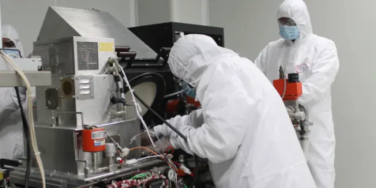
SiC Seeding for Sustainable Green Energy: An Overview of SiC Crystal Growth and Wafer Processing
Silicon carbide (SiC) is rapidly emerging as a game-changing material in the semiconductor industry. Its superior performance in high-power applications — such as electric vehicles, power grids, and renewable energy — sets it apart from traditional silicon-based solutions. With a wide bandgap, high electron mobility, and excellent thermal conductivity, SiC enables more efficient power devices, reducing energy loss and enhancing performance.
This article explores SiC crystal growth and wafer processing techniques, shedding light on the challenges and innovations driving the scalability and cost-effectiveness of SiC semiconductor manufacturing.
1. Fundamentals of SiC Crystal Growth and Material Properties
1.1 SiC Requirements
SiC is integral to modern power applications due to its exceptional properties, including a bandgap three times wider than silicon and a significantly higher critical electric field. These characteristics enable SiC-based power devices to operate at higher voltages and temperatures while reducing power losses and heat dissipation requirements.
Orbit & Skyline Semiconductor Fab Services specializes in precision processing and advanced fabrication solutions tailored for SiC technology, ensuring high-performance outcomes for semiconductor manufacturers.
1.2 SiC Crystal Structure
Silicon carbide exists in over 250 polytypes, each with unique electrical properties. Among them, 4H-SiC is the most favored due to its high electron mobility, breakdown voltage, and thermal conductivity. However, growing SiC crystals at industrial scales presents significant challenges, primarily due to the high processing temperatures (exceeding 2000°C) and the slow growth rates required to maintain quality and minimize defects.
1.3 SiC Boule Growth Methods
The semiconductor industry primarily employs three major methods for growing SiC boules, with the Physical Vapor Transport (PVT) method being the most prevalent. PVT relies on sublimation due to the lack of a stable liquid phase for SiC. Despite its advantages, challenges such as micropipes, stacking faults, and dislocation densities persist.
Orbit & Skyline’s process engineering team optimizes growth techniques to maximize yield and reduce defects, ensuring superior wafer quality. By fine-tuning parameters such as temperature control and pressure regulation, we enhance SiC crystal production efficiency.
1.4 Physical Vapor Transport (PVT) Process
The PVT process involves melting high purity SiC powder in a growth chamber at temperatures exceeding 2000°C. The sublimated vapor then deposits onto a seed crystal, gradually forming a high-quality SiC boule. This method enables precise control over doping levels, essential for tailoring electrical characteristics. N-type doping (typically using nitrogen) enhances conductivity, while p-type doping (using aluminium) influences the polytype formation, affecting overall device performance.
2. From Boule to Epi-Ready Wafer
2.1 SiC Hardness and Processing Challenges
SiC is one of the hardest materials known, ranking 9–9.5 on the Mohs scale. This extreme hardness complicates the slicing and processing of SiC boules into wafers. Specialized grinding, lapping, and polishing techniques are required to achieve the precise dimensions necessary for semiconductor applications.
Orbit & Skyline’s Equipment Engineering services provide tailored solutions to overcome these challenges, ensuring precise wafer preparation for further processing.
2.2 Wafer Slicing and Surface Preparation
SiC boules undergo slicing using multi-wire saws coated with diamond slurry. This process must balance kerf loss (material waste) and throughput efficiency. Following slicing, wafers undergo lapping to ensure uniform thickness and surface quality, crucial for subsequent epitaxial growth.
2.3 Epi-Ready Polishing and Surface Finishing
To achieve EPI-ready surfaces, wafers undergo Chemical Mechanical Polishing (CMP), combining mechanical abrasion with chemical etching. Innovations in CMP technology, such as rapid thinning techniques, enhance material removal rates while maintaining surface integrity. This ensures defect-free epitaxial layers, which are critical for high-performance semiconductor applications.
3. Epitaxial Growth and Doping of SiC
3.1 High-Temperature Chemical Vapor Deposition (HT-CVD)
Epitaxial growth involves depositing thin, defect-free SiC layers on wafers to enhance electrical performance. HT-CVD is the industry standard, offering precise control over doping concentration and layer thickness. By using silicon and carbon precursors, diluted in hydrogen or argon carrier gases, HT-CVD facilitates uniform SiC layer growth.
3.2 Alternative Epitaxy Methods
Other epitaxy methods, such as Molecular Beam Epitaxy (MBE) and Liquid Phase Epitaxy (LPE), have been explored. However, challenges in impurity control, growth rate limitations, and scalability make HT-CVD the preferred approach for large-scale SiC production.
3.3 Scaling to 8” and 200mm Wafers
With the industry shifting towards 8” (200mm) SiC wafers, significant improvements in slicing and polishing processes have been made. Advanced wafer thinning and surface finishing techniques ensure high yield and minimal defect rates. The transition to larger wafers increases device yield per wafer while optimizing fabrication costs.
Conclusion
SiC wafer technology continues to evolve, with advances in boule growth, wafer slicing, and epitaxial deposition driving the transition from 6” to 8” wafers. The industry’s focus on improving material quality and reducing processing costs ensures that SiC remains a competitive alternative to silicon in high-power applications.
Orbit & Skyline brings 15+ years of expertise, and a global team of 500+ engineers dedicated to advancing semiconductor technologies. As a trusted partner in the industry, we provide innovative solutions for SiC processing, fabrication, and equipment engineering.
For partnership inquiries, reach out to us at [email protected]
#semiconductor#Top Semiconductor Companies in India#Semiconductor Companies#Semiconductor Fab#Process Engineer
1 note
·
View note