#3D surface etching
Explore tagged Tumblr posts
Visit Tumblr Blog
Explore Tumblr blogs with no restrictions, modern design and the best experience.
Last Seen Tumblr Blogs


Fun Fact
The Tumblr app for Google Glass was released on May 16, 2013.
Text
Precision Goals: Football Moulds Transformed with Chemical Etching!
In the dynamic world of sports equipment manufacturing, precision and innovation are the key players shaping the game. The realm of football, a sport known for its passion and precision, is witnessing a transformative evolution in the production of football moulds, thanks to the art and science of chemical etching. This process, akin to laser printing on metals, is pushing the boundaries of design possibilities and elevating football moulds with 3D surface etching.
The Chemistry of Precision: Understanding the Etching Process:
At the heart of this transformation lies the meticulous process of chemical etching. Unlike traditional mechanical methods, chemical etching is a subtractive manufacturing process that involves the controlled removal of material from the surface of a metal substrate. This precision-driven method allows for the creation of intricate patterns, textures, and designs on football moulds with unparalleled accuracy.
The etching process begins with applying a photoresist material on the metal surface, protecting specific areas from chemical exposure. A design template is then transferred onto the photoresist, and the metal is exposed to a chemical solution that selectively removes material, unveiling the desired pattern or texture. The result is a precisely etched surface that contributes to both the aesthetic and functional aspects of the football mould.
Laser Precision, Chemical Artistry: Akin to Laser Printing on Metals:
Drawing parallels with laser printing on metals, chemical etching shares a commitment to precision. Laser printing and chemical etching both leverage cutting-edge technologies to achieve fine details and intricate designs. However, while laser printing involves additive processes, chemical etching is subtractive, offering a different set of advantages and design possibilities.
Chemical etching provides football manufacturers with the flexibility to create highly detailed and complex designs, including logos, player signatures, or textured surfaces for improved grip. The precision achieved through chemical etching ensures that the final product not only meets but exceeds the stringent standards set by the football industry.
Beyond Flat Surfaces: Unlocking Design Depth with 3D Surface Etching:
Taking precision and design possibilities to new heights, 3D surface etching is a game-changer in football mould production. This advanced technique allows for the creation of textured, three-dimensional surfaces on footballs, adding depth and realism to the design.
Incorporating 3D surface etching into football moulds brings a tactile element to the game. Whether mimicking the texture of traditional leather or introducing innovative patterns for enhanced aerodynamics, 3D surface etching adds a layer of sophistication and functionality to footballs. This level of detail ensures that the football not only looks remarkable but also performs optimally on the field.
Competitive Edge and Customization:
Football manufacturers adopting chemical etching in the production of football moulds gain a competitive edge in the market. The ability to offer customized footballs with intricate designs and 3D surface etching opens up new opportunities for collaborations with teams, sponsors, and events. Footballs become more than just sporting equipment; they become unique expressions of identity, branding, and innovation.
Conclusion: Precision Redefined, Innovation Unleashed:
As the football industry evolves, the integration of chemical etching into the production of football moulds is a testament to the marriage of precision and innovation. Similar to the finesse of laser printing on metals, chemical etching is reshaping the aesthetics and performance of footballs. With the added dimension of 3D surface etching, footballs are poised to reach new levels of design sophistication and functionality, kickstarting a new era of precision in the game we love.
0 notes
Text

Laser Engraving on Mixer Jar Lid Molds: Combining Precision and Elegance
Experience precision and elegance in laser engraving for mixer jar lid molds, blending advanced technology with refined design for superior performance and style.
#3D laser engraving#Laser Engraving#Mould Surface textures service provider#Mould Polishing#laser etching companies#laser etching
0 notes
Text

Novel etching technique enhances absorptivity of powders for metal 3D-printing
In a significant advancement for metal additive manufacturing, researchers at Lawrence Livermore National Laboratory (LLNL) and their academic partners have developed a technique that enhances the optical absorptivity of metal powders used in 3D printing. The approach, which involves creating nanoscale surface features on metal powders, promises to improve the efficiency and quality of printed metal parts, particularly for challenging materials like copper and tungsten, according to researchers. Additive manufacturing (AM)—more commonly known as 3D printing—has transformed the way products are designed and produced, allowing for the creation of complex geometries and customized components that traditional manufacturing methods struggle to achieve.
Read more.
#Materials Science#Science#Powder#3D printing#Additive manufacturing#Etching#Absorptivity#Metals#Copper
13 notes
·
View notes
Text
Techniques and craftmanship methods require for Jewelry making
Jewelry making involves a wide range of techniques and craftsmanship methods, each requiring specific skills, tools, and materials. Here are some of the most common techniques used in jewelry making, whether for handmade artisanal pieces or mass-produced collections:
Hand Fabrication
Sawing: Using a jeweler’s saw to cut metal sheets into desired shapes.
Filing & Sanding: Smoothing and refining metal surfaces or edges after cutting.
Soldering: Using heat to melt solder (a metal alloy) to join pieces of metal, such as attaching clasps, links, or settings.
Forging: Shaping metal by hammering it to create texture, thin it out, or curve it.
Polishing: Using buffing machines, wheels, or cloth to achieve a high-shine finish on the metal.
Casting
Lost Wax Casting: A mold is created from a wax model, which is then melted and replaced with molten metal. This is one of the oldest techniques used for making detailed metal jewelry pieces.
Centrifugal & Vacuum Casting: Used to ensure the molten metal flows evenly into the mold, minimizing air bubbles and imperfections.
Stone Setting
Prong Setting: Small metal prongs are used to hold a gemstone in place. Common for engagement rings.
Bezel Setting: A metal rim encircles the gemstone to hold it securely.
Pavé Setting: Multiple small gemstones are set closely together, often giving the illusion of a continuous surface of stones.
Channel Setting: Gemstones are set between two strips of metal, allowing for a seamless, smooth look.
Flush Setting: The gemstone is set flush with the metal surface, offering a sleek and modern aesthetic.
Gypsy Setting: Similar to flush setting but usually involves a hammered finish around the gemstone, used for bold, simple designs.
Engraving & Embellishment
Hand Engraving: Using sharp tools to carve intricate patterns or designs into metal surfaces.
Laser Engraving: A modern technique that uses lasers to create detailed engravings or inscriptions, often used for personalization.
Etching: Using acid or other chemicals to corrode the surface of the metal in specific patterns, creating a textured or detailed design.
Filigree
Wire Work: Fine wires of gold or silver are twisted and shaped into intricate designs, often with lace-like appearances. This technique requires high precision and is often used in traditional jewelry.
Enameling
Cloisonné: Small cells or compartments are created with metal wire, which are then filled with enamel (colored glass powder) and fired to create vibrant patterns.
Champlevé: Enamel is applied into recessed areas of metal, then fired to create a colored design.
Plique-à-Jour: A transparent enamel technique that allows light to shine through, giving a stained-glass effect.
Hammering & Texturing
Chasing: A technique where the surface of the metal is hammered from the front to create patterns or designs.
Repoussé: The reverse of chasing, where the metal is hammered from the back to create a raised design.
Texturing: Using different hammers, stamps, or other tools to create a variety of surface textures, such as hammered, brushed, or matte finishes.
Wirework
Wire Wrapping: Jewelry made from twisting and wrapping wire into shapes and loops, often around gemstones, beads, or crystals.
Weaving & Knotting: Using wire or string to weave intricate patterns, often incorporating beads or small stones.
Beadwork
Stringing: Threading beads, pearls, or gemstones onto a string or wire to create necklaces or bracelets.
Knotting: Tying knots between beads (commonly pearls) to ensure they don’t rub against each other and for added strength.
Loom Beading: Using a loom to weave tiny seed beads into patterns for bracelets, necklaces, or other accessories.
Electroforming
Metal Coating: This is a process where a base material (such as a wax or organic object) is coated with a metal layer through electroplating. It’s commonly used for creating lightweight, hollow jewelry pieces.
CNC & 3D Printing
CNC Machining: This computerized technique is used to carve precise patterns and designs into metal or wax, enabling intricate designs that are difficult to achieve by hand.
3D Printing: Used for prototyping or creating complex designs, 3D printing involves creating a wax or resin model layer by layer, which can then be cast in metal using traditional techniques.
Inlay & Marquetry
Stone Inlay: Stones, such as turquoise or lapis lazuli, are cut into thin pieces and inserted into metal grooves to create decorative designs.
Wood or Shell Inlay: Wood, shell, or other non-metal materials are inlaid into metal surfaces to create intricate designs or mosaics.
Embossing & Stamping
Stamping: Using metal stamps or dies to create patterns or letters on the surface of a piece.
Embossing: Using pressure to raise designs on metal surfaces, creating a three-dimensional effect.
Granulation
Beading Technique: Small metal beads or granules are applied to the surface of a piece and soldered to create intricate designs, often used in ancient and traditional jewelry styles.
Soldering & Welding
Soldering: Used to join metal pieces together with the help of solder and heat.
Laser Welding: A modern technique using laser technology to weld small or delicate pieces of metal together, often for intricate repairs.
Pearl & Bead Setting
Knotting: Hand-knotting is used in pearl necklaces to separate each pearl and add durability.
Glue Setting: Some beads and pearls are set using adhesives, especially in designs where drilling holes isn't practical.
By mastering these techniques and methods, jewelry makers can produce pieces ranging from simple, minimalist designs to complex, ornate creations. The choice of technique depends on the desired aesthetic, materials used, and the skill level of the jeweler.
5 notes
·
View notes
Text
Visiting The Titanic Is Suddenly A Lot Easier Than You Think
Fresh Advances in 3D Scanning Technology are Making It Possible to Explore Some of the Hardest-to-Reach and Most Fragile Sites on Earth.
— By Camille Bromley | April 8, 2025

This rendering of the Titanic is based on 715,000 photos and millions of laser scans of the famous wreck, which were stitched together to create a perfect digital replica of what remains of the ship. Image By Magellan Limited/Atlantic Productions
Last year, Parks Stephenson stood next to the Titanic and walked slowly around it, gazing up at the massive ship. He paused to look inside one of the boiler rooms and at the position of the controls on the engines. He noticed the number 401, the ship’s ID, etched on the propeller blades. Rusticles hung from the steel shell. Twisted metal and personal trinkets from those long dead littered the ground.
Stephenson, a retired naval officer and Titanic historian, wasn’t 12,500 feet below the surface of the North Atlantic, of course. He was in London, inspecting the ship’s digital twin: a one-for-one computer model made possible by advances in remote 3D scanning and mapping technology. The model is so densely detailed, a video rendering of it can be projected to life-size in a warehouse, where researchers can walk alongside it and zoom in and out on individual features, like a steam valve from the boiler room, which the scan revealed was left open, possibly to keep an emergency generator running as the ship sank. The Titanic twin adds to a growing list of similar models made of archaeological and cultural sites around the world that both preserve these fragile places and provide a new means of exploring them.
Stephenson has seen the actual Titanic wreck twice since his first dive in 2005, but he didn’t catch so many details on his trips. “You can only see what’s immediately in front of you,” he says of peering through a submersible’s roughly six-inch viewport and camera views. “It’s like being in a dark room and you have a flashlight that’s not very powerful.” The digital twin, on the other hand, gave him an unobstructed, 360-degree view of every gnarled nook and cranny.
The scan of the storied ship was carried out over three weeks in 2022 by Magellan, a deep-sea mapping company based in the Channel Islands. Titanic: The Digital Resurrection, a new National Geographic documentary streaming on Disney+, tells the story of the effort. It is the largest underwater 3D scan ever made, amounting to 16 terabytes of data (equivalent to the hard drive footprint of six million e-books). To create it, two remote-operated robots romantically named Romeo and Juliet traveled down to the wreck and systematically canvassed the site, taking some 715,000 photos and millions of laser measurements.
For Stephenson, the quality of detail in the scan opens new lines of inquiry into the sinking of the Titanic. The ship lies broken in two pieces, with the bow and stern about 2,600 feet apart. The hull descended in a straight line and is largely still intact—the scan shows it neatly wedged into the ocean floor. The stern, on the other hand, is shattered, and researchers have never been able to definitively say how that happened. When Stephenson looked at the scan, though, he could immediately envision the back half of the ship spiraling as it sank and disintegrating into rubble. “At a first glance,” he says, “it just made sense.”
In the past, a full, grand scale of the wreck could be depicted only through artistic renditions or photomosaics created by humans. Neither method conveyed precise verisimilitude. The machine-run 3D model, however, is exact. “As soon as I saw the Titanic digital twin images,” Stephenson says, “I could tell. Number one, I’d never seen Titanic like this before. And number two, it felt right.”

More scientists are using digital replicas to allow the study of everything from artifacts to human remains—like this ancient Nepalese child’s skull—without damaging them. Photograph Courtesy Julia Gresky, German Archaeological Institute (DAI)
The quest to create exact models for more accessible surveying started over a century ago. The technology that makes digital twinning possible dates back to at least 1858, when a German engineer named Albrecht Meydenbauer was tasked with surveying a church and nearly fell to his death while measuring the facade. To avoid another dangerous climb, he worked out a way to mathematically calculate the measurements of large objects from photos—a technique he called photogrammetry. Today photogrammetry combined with lidar, which uses lasers to measure distances, as well as advanced computing power, produces models that can accurately replicate the most minute details of enormous structures like Mount Rushmore or the aesthetic proportions of Michelangelo’s “David.”
The Italian Renaissance master’s sculpture was one of the first major artifacts to be digitally modeled, in 2000, by Stanford University. Though not as massive as the Titanic, the statue’s relatively large size—17 feet tall and 12,500 pounds—and finely chiseled details made it a good test for how accurately 3D technology might reproduce objects on a grand scale. Today the tech is so precise that in 2020 a team at the University of Florence produced a 3D-printed copy, accurate down to David’s resolute expression and every defect of the original stone.
People travel to see masterpieces of human creativity because they want to feel the presence of something awesome or genius. But too much of our presence can destroy places that are irreplaceable. Hundreds have visited the Titanic, most of them at enormous expense, including five on the ill-fated Titan submersible. These explorers are the source of significant damage suffered by the wreck; human-piloted submersibles have inadvertently stripped a mast and gashed the bow.
Beyond tourism, sites may be unpredictably damaged by natural disasters, climate change, or war. In 2019, 3D documentation company CyArk created models of Nigeria’s Osun-Osogbo Sacred Grove, just before the sculpture-laden forest shrines were destroyed in a flood. Chance Coughenour, a program manager for Google Arts & Culture, which supported CyArk in these efforts and hosts these models online, hopes the shrines can be rebuilt from the scans. Coughenour’s group supported similar efforts to create digital twins of a cathedral and a historic government landmark in Ukraine that are now damaged by the war.


Treasured cultural sites, like St. George’s Cathedral, a World Heritage site in Lviv, Ukraine, have been digitized inside and out. If they are ever damaged by climate change, a natural disaster, or war, they can be rebuilt from the copy. Photograph By Matt Propert; Rendering By Andriy Hryvnyak, SkeIron
On an even grander scale, digital twins can be made of not only buildings, statues, and shipwrecks but also entire cities—living or dead. Allison Emmerson, an archaeologist at Tulane University, is making a digital twin of parts of Pompeii, a famously fragile site where she’s spent the past 16 years digging through layers of soil to uncover the city’s earliest history. Emmerson says digital twinning is the biggest leap forward for archaeology since photography. “Our process is inherently destructive,” she says of excavating a site. “We can never redo it. We can dig the site once. And so the focus in modern archaeology has been on recording as well as we possibly can.”
Her team’s twin of a block in the southeast of the city was made with just a few handheld cameras. The model allows them to visualize the site with the walls of a room taken away, or a roof added, or how the land looked before the building was constructed. They can call up the model back in the lab and continue conversations that previously would happen only in the field. Emmerson’s work has revealed how one building at the site was both a restaurant and a workshop where people manufactured reed baskets and mats—details that help her understand the city’s economy and the daily life of its working class.
For Her Part, Emmerson plans to make her model of Pompeii and the accompanying findings available to the public, avoiding a common outcome for these projects. Because digital twins are expensive to create, many ambitious projects end up locked way in the private archives of universities or governments. “I did not want the model to live on a team member’s laptop,” she says.
While Magellan has not announced any plans to make its Titanic scans free to the public, the documentary itself shows what’s possible. Much of the existing research on the shipwreck has been conducted by private expeditions that guard findings, an ongoing source of concern for scientists and citizen enthusiasts alike. Stephenson remains concerned the wreck is not being treated as an archaeological site. “It’s one of the most famous sites in the world, and we don’t even have the basic baseline information needed to establish what’s there at any particular time, because you’ve had different explorers who don’t share information,” he says. The digital twin has the potential to allow more visitors to experience it in a less destructive and more collaborative way.
It’s unlikely people will stop going to the Titanic wreck site. Its draw has proven irresistible for those with enough money and motivation. In 2001, for example, a couple exchanged vows crouched in a submersible perched on the bow. A digital twin “certainly doesn’t replace sitting on the deck of the Titanic,” says Robert Ballard, an oceanographer and National Geographic Explorer at Large who discovered the wreck in 1985 along with Jean-Louis Michel. But he thinks it will help preserve the wreck. For those who cannot resist going themselves, he offers two warnings: “Don’t touch it. Don’t get married on it.”
youtube
#Youtube#Titanic#3D Scanning#Shipwrecks#Archaeology#Underwater Archaeology#Ruins#Exploration#Hardest-to-Reach Areas#Fragile Sites#Planet Earth 🌍#National Geographic#Camille Bromley
2 notes
·
View notes
Text

3D Material workshop Concept development:
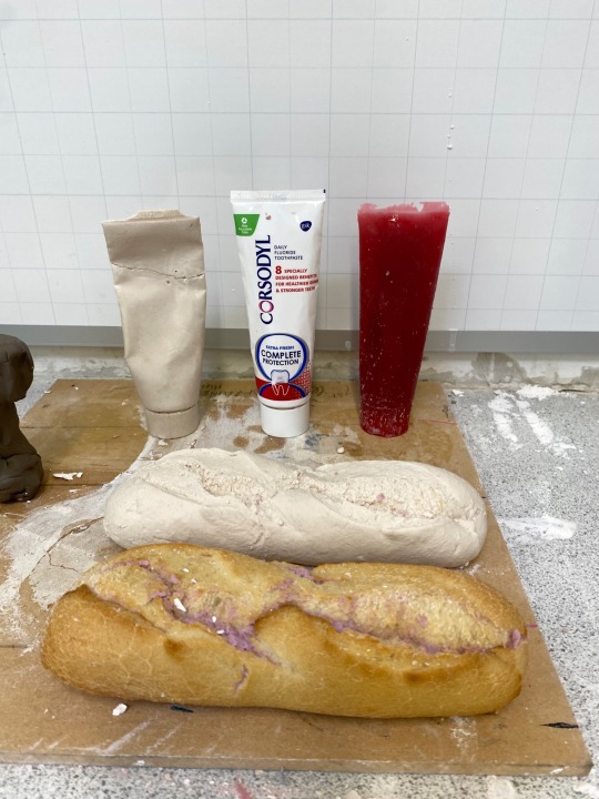
During the week I met with Ashling for a peer review meeting. I explained my idea of looking at not necessarily disrupting things but how things that cant speak say so much about disruptions. I explained that I came home one weekend and when I went to the bathroom I saw two tubes of toothpaste a a ring that marked where the third one used to lie. I knew at that moment I was in for a quiet weekend. I did not know where the other girl had gone but from one item missing in our busy house I knew there was going to be a weekend free of arguments and disruption. We decided it would be interesting to cast some tubes of toothpaste. I wanted one that was full and one that was squeezed empty. I would like to place them together next to a ring of toothpaste that can imply the third and final toothpastes existence. The remaining two toothpastes belong to two girls who have a beautiful, long friendship or supporting each other through thick and thin. The empty(ish) tube of toothpaste is mine. I am so poor (I love college but I am so poor) and every time I look at my toothpaste I am just determined to squeeze more out of it because if I give up looking after my teeth and keep smoking I'll grow up and they'll all fall out. The other tube belongs to my beautiful house mate. Even though its full (because shes working full time) she is running on empty (emotionally). I know that seems like a big long ramble but being this age is so difficult. There is so much to do everyday and thats ignoring all the time it takes to attend to your basic needs. Taking that time each day can feel so exhausting but every time I do it I try and think of how this disruption will be worth it in the long run. I also think its so interesting and strangely insightful to look at different objects that belong to very different people and see the level of giving a fuck to these annoying disruptions they give. I don't know if people are aware of this but Corsadyl is expensive but my dentist (also expensive) told me to use it. Maybe the crack in the tube a represent the disruption to my bank account its causing.
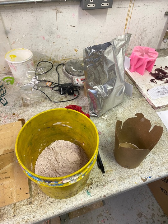
Casting process: We decided to use Alginate with is a seaweed powder that gets mixed with water (water is poured onto the powder, always). I glued the tube of toothpaste to a board and attached a cylinder piece of card around it and poured the mixture in. It sets in about 4 minutes and then you're ready to take the object out and mix up some plaster to create the piece. Below is a video of me chuffed pulling the toothpaste out.


I understand how influential art is and how it's crafts and skills that are taken seriously to move people into thinking, feeling and questioning, but, if you can't tell from this video I was actually just having so much fun with this whole process.
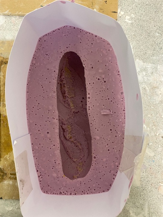
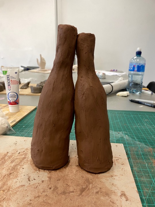
Afterwards I repeated the same process but casted a bread roll (another staple and I know its weird to put bread in the fridge but food goes off so fast and bread just lasts longer if you keep it in the fridge and I have no time to go to Lidl more than once a week). The mould looked good so I mixed up some plaster. Mixing plaster is the opposite to mixing Alginate as you start with water and slowly add the plaster powder in. You fill your mould with water and then you pour that into a bowl so you have an idea of how much plaster you'll need. You slowly add the powder in in circular movements until it started to sit on the top. Then (and only then) can you stir it gently by placing your hand in and mixing under the surface. If you're taking your hand in and out you're going to add air in and you don't want air bubbles in your piece so you have to be gentle and careful. For the full tube of toothpaste I did a wax cast because i wanted to try a different material. I wasn't happy with how it looked because it doesn't really look like toothpaste but I might etch some toothpaste resembling things (disrupt the surface) onto it so the viewer knows its toothpaste. I wanted to use red wax because I thought it would be an interesting way to demonstrate that just because you're put together enough to regularly restock your toothpaste does not mean you are physically and mentally doing so great. These are the final pieces. I but the bread roll back into the bag I bought it in and I'm chuffed with how it turned out. For the afternoon I made some beer bottles that and delicately kissing. I would rather talk about this subject in person.
7 notes
·
View notes
Text

Subsurface laser engraving is a modern technique that creates breathtaking 3D designs inside crystals without damaging the surface. Crystal Sensation Subsurface laser engraving specializes in delivering precision-crafted, high-quality 3D crystal gifts using this advanced method. Whether for corporate awards, personal keepsakes, or special events, Crystal Sensation ensures each piece is intricately detailed and beautifully preserved. This unique engraving process uses laser technology to etch images beneath the surface, offering a lasting, elegant finish. Customers choose Crystal Sensation for its exceptional craftsmanship, cutting-edge equipment, and personalized service. Subsurface laser engraving makes it possible to capture memories in a timeless crystal form. Trust Crystal Sensation to transform your favorite photos and designs into stunning crystal masterpieces that leave a lasting impression.
0 notes
Text
Silicon Rings and Silicon Electrodes for Etching Market: Size, Growth, and Key Players

MARKET INSIGHTS
The global Silicon Rings and Silicon Electrodes for Etching Market size was valued at US$ 234 million in 2024 and is projected to reach US$ 321 million by 2032, at a CAGR of 4.6% during the forecast period 2025-2032.
Silicon rings and electrodes are critical consumable components used in plasma etching systems for semiconductor manufacturing. These high-purity silicon parts ensure uniform electrical properties during the etching process, primarily for 8-inch to 12-inch (200mm-300mm) wafers. The components require frequent replacement due to wear – a silicon ring typically needs replacement after processing approximately 200 wafers, making them recurring revenue drivers in semiconductor fabrication.
Market growth is fueled by increasing semiconductor demand across industries, particularly in IoT, AI, and 5G applications. The transition to larger wafer sizes and advanced process nodes further boosts consumption. North America currently dominates production with 60% market share, while China shows the fastest growth potential. Major players like Silfex and Hana Materials collectively hold 85% market revenue, with OEM customers accounting for 70% of sales. Twelve-inch silicon components lead the market with 80% share as semiconductor fabs continue scaling up production capacity.
MARKET DYNAMICS
MARKET DRIVERS
Rising Semiconductor Manufacturing Investments Accelerate Demand for Silicon Components
The global semiconductor industry is experiencing unprecedented growth, with fab construction projects reaching record levels. Over 90 new semiconductor manufacturing facilities are projected to begin operations between 2021 and 2025, creating sustained demand for consumables like silicon rings and electrodes. As chipmakers transition to more advanced nodes below 7nm, the precision requirements for plasma etching processes have intensified, directly increasing the consumption rate of these critical components. The average replacement cycle for silicon rings has decreased by approximately 30% for advanced node manufacturing compared to mature processes, driving recurring revenue streams for manufacturers.
Transition to Larger Wafer Sizes Fuels Market Expansion
The industry’s ongoing shift toward 12-inch (300mm) wafer production represents a key growth driver, with these larger formats now accounting for over 80% of silicon component demand. This transition requires entirely new production lines with significantly different specifications compared to 8-inch equipment. Each 300mm plasma etcher requires approximately 35-50% more silicon material per component than their 200mm counterparts. Furthermore, the precision tolerances for 300mm components are typically 40% tighter, creating opportunities for manufacturers capable of meeting these exacting standards. The market for 300mm silicon rings and electrodes is projected to grow at nearly 12% annually through 2030.
Advanced Packaging Technologies Create New Application Avenues
Emerging 3D packaging techniques like chiplet architectures and through-silicon vias (TSVs) are driving innovation in etching processes and component requirements. These next-generation packaging approaches demand specialized etching procedures that place unique stresses on silicon consumables. Manufacturers developing components with modified silicon grain structures and specialized surface treatments are positioned to capture this growing segment. The advanced packaging market for silicon components is expected to exceed $450 million annually by 2027 as chipmakers increasingly adopt heterogeneous integration strategies.
MARKET RESTRAINTS
Supply Chain Constraints Limit Production Capacity Expansion
The specialized polysilicon feedstock required for high-purity components faces severe supply limitations, with lead times extending beyond 9 months for certain grades. This bottleneck is compounded by the concentration of raw material suppliers in restricted geographic regions, creating vulnerability to geopolitical disruptions. Component manufacturers report difficulty securing consistent supplies of 11N purity silicon, which is essential for meeting semiconductor industry specifications. The supply-demand imbalance has led to price volatility exceeding 35% for some silicon feedstocks over the past two years.
Technical Challenges in Advanced Node Manufacturing Constrain Yields
As semiconductor processes advance below 5nm, etching uniformity requirements have become exponentially more stringent. Current generation silicon components struggle to maintain the sub-nanometer surface uniformity needed for these cutting-edge applications. The transition to new architectures like gate-all-around transistors introduces plasma loading effects that reduce average component lifespan by up to 40%. These technical challenges have created a performance gap between existing solutions and industry needs, particularly for EUV patterning applications where etch uniformity directly impacts overlay accuracy.
High Capital Investment Requirements Deter New Market Entrants
The specialized equipment and cleanroom facilities needed for silicon component manufacturing represent a significant barrier to entry, with new production lines requiring investments exceeding $150 million. Precision machining centers for 300mm components alone can cost over $25 million per unit, while the qualification process for new semiconductor-grade products typically takes 18-24 months. These financial and temporal commitments have limited market participation to established players with existing semiconductor industry relationships, slowing the pace of innovation in key areas like alternative materials and coating technologies.
MARKET OPPORTUNITIES
Development of Composite and Coated Solutions Presents Innovation Potential
Emerging hybrid materials combining silicon with specialized coatings or reinforcement phases offer significant performance improvements. Early adopters of silicon carbide-coated electrodes report 60-80% longer service life in demanding plasma environments while maintaining critical electrical properties. The market for enhanced silicon components incorporating advanced surface treatments is projected to grow at 15% annually through 2030. Companies investing in material science R&D are positioned to capture premium pricing opportunities in this segment, particularly for high-volume logic and memory applications.
Regional Semiconductor Self-Sufficiency Initiatives Create Localization Opportunities
Government policies promoting domestic semiconductor supply chains are driving localized component procurement strategies. The CHIPS Act in the United States and similar programs in Europe/Asia have earmarked over $20 billion specifically for materials and equipment localization. Manufacturers establishing regional production footprints near major semiconductor clusters can benefit from these incentives while reducing logistical challenges. The localization trend is particularly strong in Southeast Asia, where new component facilities are being developed to support the region’s growing share of global semiconductor manufacturing capacity.
AI-Driven Predictive Maintenance Opens New Service Models
Advanced analytics platforms capable of predicting silicon component end-of-life with over 90% accuracy are transforming maintenance strategies. These systems leverage real-time process data from plasma etchers to optimize replacement schedules, reducing unplanned downtime by up to 35%. Forward-thinking manufacturers are bundling predictive analytics with their consumable products, creating recurring revenue streams while strengthening customer relationships. The integration of IIoT capabilities into next-generation components could further enhance these service offerings, potentially increasing customer willingness to pay premium pricing for smart components.
MARKET CHALLENGES
Intellectual Property Protection Concerns in Emerging Markets
The expansion of manufacturing capacity in regions with less robust IP protection frameworks poses significant risks. Competitor analysis reveals reverse-engineered components entering certain Asian markets within 12-18 months of new product launches. These unauthorized products typically compromise on quality but undercut pricing by 40-60%, eroding profit margins for innovators. Companies must balance the need to participate in growing regional markets with the protection of proprietary manufacturing know-how. The increasing complexity of component designs for advanced nodes may help mitigate this risk by raising the technical barriers to duplication.
Process Integration Challenges at Advanced Nodes
The transition to cutting-edge semiconductor technologies introduces unforeseen interactions between silicon components and new process chemistries. Recent challenges include unexpected erosion patterns when using high-k dielectric etchants and plasma-induced crystallization changes affecting doping uniformity. Each new process node requires extensive requalification of consumable components, stretching development timelines and increasing R&D costs by approximately 25% per generation. Component manufacturers must maintain close technical collaboration with equipment OEMs and chipmakers to proactively address these emerging technical hurdles.
Environmental Regulations Impact Manufacturing Processes
Evolving environmental standards are imposing new constraints on silicon component production. Restrictions on certain etching byproducts and abatement system requirements have increased production costs by 12-15% at major facilities. The transition to greener manufacturing processes requires significant capital investment, particularly for wastewater treatment systems capable of handling advanced cleaning chemistries. While sustainability initiatives present long-term benefits, the near-term compliance costs represent a meaningful challenge for manufacturers operating on thin margins in highly competitive markets.
SILICON RINGS AND SILICON ELECTRODES FOR ETCHING MARKET TRENDS
Expansion of Semiconductor Manufacturing to Drive Silicon Components Demand
The rapid growth in semiconductor manufacturing, particularly for advanced-node chips, is accelerating the adoption of silicon rings and electrodes in plasma etching applications. With the global semiconductor industry projected to exceed $1 trillion by 2030, the demand for high-purity silicon consumables has surged to enable precise wafer processing. Semiconductor fabricators are increasingly adopting 300mm wafer technology, where silicon components demonstrate superior plasma uniformity compared to traditional materials. This shift has led to approximately 85% market dominance for 12-inch components as manufacturers prioritize yield optimization.
Other Trends
Localization of Semiconductor Supply Chains
Geopolitical considerations and supply chain resiliency concerns are prompting regional silicon component production shifts. While North America currently maintains 60% production share, China’s semiconductor ecosystem development is driving rapid capacity expansion, with domestic silicon component manufacturing expected to grow at double-digit rates through 2030. This localization trend is particularly evident in memory production hubs, where Korean manufacturers are vertically integrating silicon consumable supplies to reduce dependency on imports.
Advancements in Component Manufacturing Technologies
Material innovation is transforming silicon component performance characteristics in plasma etching applications. Leading manufacturers are developing composite-doped silicon materials that extend component lifespan while maintaining plasma stability. Recent process improvements have enhanced surface finishing techniques, reducing particle generation during etching operations. This technological evolution has enabled replacement intervals to stretch beyond 300 wafers in some applications, representing a 50% improvement over previous-generation components.
The industry is also witnessing increased adoption of predictive maintenance systems that monitor silicon component wear patterns. These AI-driven solutions analyze historical etch rates and plasma parameters to optimize replacement schedules, significantly reducing unplanned tool downtime. Such technological integration is becoming a key differentiator as semiconductor manufacturers prioritize fab productivity.
COMPETITIVE LANDSCAPE
Key Industry Players
Market Leaders Expand Production Capacity Amid Surging Semiconductor Demand
The global silicon rings and electrodes for etching market exhibits a semi-consolidated structure, dominated by specialty material suppliers with vertically integrated semiconductor solutions. Silfex Inc. (a subsidiary of Lam Research) leads the competitive landscape, leveraging its precision machining capabilities and direct access to major chip manufacturers across North America and Asia. The company’s market position stems from its ability to deliver ultra-high purity silicon components meeting stringent semiconductor fabrication requirements.
Hana Materials Inc. maintains a strong second position, particularly in the South Korean market where it supplies major semiconductor equipment OEMs. Their growth reflects the broader industry trend toward localized supply chains in key chip manufacturing hubs. Meanwhile, CoorsTek has been expanding its market share through strategic acquisitions and technological partnerships, particularly in advanced ceramics-silicon hybrid components.
Recent investments highlight intensifying competition. Mitsubishi Materials committed $120 million in 2023 to expand silicon component production capacity in Japan, while SK Enpulse completed a new automated manufacturing facility in South Korea. These developments indicate how market leaders are preparing for the projected 8.9% CAGR through 2032, with particular focus on 12-inch wafer solutions that currently dominate 80% of demand.
List of Key Silicon Components Companies Profiled
Silfex, Inc. (U.S.)
Hana Materials Inc. (South Korea)
CoorsTek, Inc. (U.S.)
Thinkon Semiconductor (China)
Worldex Industry & Trading (South Korea)
Grinm Semiconductor Materials (China)
Mitsubishi Materials Corporation (Japan)
SK Enpulse (South Korea)
BASi Research Products, Inc. (U.S.)
DynafineSemi (China)
Segment Analysis:
By Type
Silicon Electrodes Segment Holds Major Share Due to Critical Role in Plasma Etching Processes
The market is segmented based on type into:
Silicon Rings
Silicon Electrodes
By Size
12 Inch Segment Dominates Market With Growing Demand for Larger Wafer Processing
The market is segmented based on wafer size into:
8 Inch (200mm)
12 Inch (300mm)
By Customer Type
OEM Segment Leads the Market as Key Component Suppliers for Semiconductor Equipment Manufacturers
The market is segmented based on customer type into:
Original Equipment Manufacturers (OEM)
Wafer Fabrication Plants
By Region
North America Maintains Production Dominance as Key Semiconductor Manufacturing Hub
The market is segmented based on production region into:
North America
Asia Pacific
Europe
Rest of World
Regional Analysis: Silicon Rings and Silicon Electrodes for Etching Market
North America North America dominates the global silicon rings and electrodes market, accounting for approximately 60% of production, with the U.S. being the primary manufacturing hub. The region benefits from strong semiconductor industry presence and technological leadership in advanced etching applications. Companies like Silfex and CoorsTek leverage local expertise in high-purity silicon manufacturing, servicing major semiconductor OEMs. While demand remains steady from established fabrication facilities, growth is tempered by market maturity and high operational costs. However, reshoring initiatives and government incentives under the CHIPS Act are creating new opportunities for domestic silicon component suppliers.
Europe Europe maintains a specialized position in the market through precision engineering capabilities, particularly in Germany and France. While production volumes are lower than Asia or North America, European manufacturers focus on high-value applications in automotive and industrial semiconductors. Strict EU regulations on material purity and manufacturing emissions influence production standards, creating barriers for new entrants but ensuring quality consistency. The region faces challenges from energy price volatility and slower adoption of next-gen fabrication technologies compared to global peers, limiting market expansion despite technological competence.
Asia-Pacific As the fastest-growing region, Asia-Pacific is transforming from a consumer to a producer of silicon etching components, led by South Korea’s 20% global production share and China’s rapid capacity expansion. The concentration of semiconductor fabs in Taiwan, South Korea, and China drives enormous demand, with local suppliers like Hana Materials gaining market share through cost competitiveness. Japan retains technological leadership in material science but faces stiff price competition. The region’s growth is propelled by national semiconductor self-sufficiency initiatives, particularly China’s push to localize 70% of its chip production by 2030, creating parallel demand for domestic silicon component suppliers.
South America The South American market remains in early development stages, with limited local production capabilities. Brazil shows nascent interest in semiconductor manufacturing, but reliance on imports persists due to infrastructure gaps and lack of specialized suppliers. While regional trade agreements facilitate component sourcing from North America and Asia, high import duties and logistical challenges increase costs for local fabricators. Market growth is constrained by political instability in key economies and limited government support for high-tech manufacturing ecosystems, relegating the region to a minor consumption market.
Middle East & Africa This emerging market is witnessing strategic investments in semiconductor infrastructure, particularly in Israel and the UAE, creating niche opportunities for silicon component suppliers. Israel’s strong tech sector drives demand for specialized etching applications, while Gulf nations aim to diversify into high-tech manufacturing. However, the lack of local silicon processing expertise and dependence on foreign technology transfers slow market development. While current consumption volumes are modest, long-term potential exists as regional governments increase STEM education investments and forge partnerships with global semiconductor leaders to build localized supply chains.
Report Scope
This market research report provides a comprehensive analysis of the global and regional Silicon Rings and Silicon Electrodes for Etching markets, covering the forecast period 2025–2032. It offers detailed insights into market dynamics, technological advancements, competitive landscape, and key trends shaping the industry.
Key focus areas of the report include:
Market Size & Forecast: Historical data and future projections for revenue, unit shipments, and market value across major regions and segments. The Global Silicon Rings and Silicon Electrodes for Etching market was valued at USD 1,597 million in 2024 and is projected to reach USD 2,869 million by 2032, growing at a CAGR of 8.9% during the forecast period.
Segmentation Analysis: Detailed breakdown by product type (Silicon Ring, Silicon Electrode), customer type (OEM, Wafer FAB), and size (8-inch, 12-inch) to identify high-growth segments and investment opportunities. 12-inch silicon components dominate with 80% market share, while OEMs account for 70% of demand.
Regional Outlook: Insights into market performance across North America (60% production share), Asia-Pacific (fastest growing), Europe, Latin America, and the Middle East & Africa, including country-level analysis of key markets like USA, South Korea, Japan and China.
Competitive Landscape: Profiles of leading market participants including Silfex, Hana Materials, CoorsTek, Mitsubishi Materials and SK Enpulse, covering their product offerings, R&D focus, manufacturing capacity, and recent developments. The top 7 players hold 85% market share.
Technology Trends & Innovation: Assessment of emerging fabrication techniques, material purity requirements, and evolving standards for semiconductor etching applications.
Market Drivers & Restraints: Evaluation of factors driving market growth (semiconductor industry expansion, wafer production increases) along with challenges (supply chain constraints, high purity material requirements).
Stakeholder Analysis: Insights for component suppliers, semiconductor equipment manufacturers, foundries, investors, and policymakers regarding the evolving ecosystem and strategic opportunities.
Related Reports:https://semiconductorblogs21.blogspot.com/2025/06/chip-solid-tantalum-capacitor-market.htmlhttps://semiconductorblogs21.blogspot.com/2025/06/global-electrical-resistance-probes.htmlhttps://semiconductorblogs21.blogspot.com/2025/06/high-temperature-tantalum-capacitor.htmlhttps://semiconductorblogs21.blogspot.com/2025/06/global-link-choke-market-innovations.htmlhttps://semiconductorblogs21.blogspot.com/2025/06/multirotor-brushless-motors-market.htmlhttps://semiconductorblogs21.blogspot.com/2025/06/planar-sputtering-target-market.htmlhttps://semiconductorblogs21.blogspot.com/2025/06/ferrite-core-choke-market-opportunities.htmlhttps://semiconductorblogs21.blogspot.com/2025/06/float-zone-silicon-crystal-market.htmlhttps://semiconductorblogs21.blogspot.com/2025/06/carbon-composition-resistors-market.htmlhttps://semiconductorblogs21.blogspot.com/2025/06/resistor-network-array-market-analysis.htmlhttps://semiconductorblogs21.blogspot.com/2025/06/melf-resistors-market-key-drivers-and.htmlhttps://semiconductorblogs21.blogspot.com/2025/06/metal-foil-resistors-market.htmlhttps://semiconductorblogs21.blogspot.com/2025/06/metal-oxidation-resistors-market-size.htmlhttps://semiconductorblogs21.blogspot.com/2025/06/ferrite-toroid-coils-market-growth.htmlhttps://semiconductorblogs21.blogspot.com/2025/06/vacuum-fluorescent-displays-market.html
0 notes
Text
Precision Play: Unveiling the Excellence of Chemical Etching in Elevating Football Moulds
In the intricate world of manufacturing, precision is the key to producing superior products that meet the highest standards. One innovation that has been making waves, particularly in the realm of football manufacturing, is the integration of chemical etching. This sophisticated process, often coupled with techniques like sandblasting and 3D surface etching, is redefining the precision and excellence achieved in crafting football moulds.
The Chemical Etching Process: A Symphony of Precision
Chemical etching is a meticulously controlled process that involves the selective removal of material from the surface of a substrate. In the context of football moulds, this process is instrumental in achieving unparalleled precision. The chemical etching process allows manufacturers to create intricate patterns, textures, and details on the mould's surface with unmatched accuracy.
Unlike traditional machining methods, chemical etching ensures a uniform and controlled material removal, eliminating the risk of distortion or damage to the delicate features of the football mould. This precision is crucial in crafting footballs with consistent seams, textures, and patterns, contributing to the overall performance and aesthetics of the final product.
Sandblasting: Texture and Grip Refinement
Complementing the precision of chemical etching, sandblasting is often employed to refine the texture and enhance the grip of football moulds. Sandblasting involves the use of high-pressure air to propel abrasive particles onto the surface of the mould. This process creates a textured finish that not only improves the grip of the football but also adds a visually appealing and tactile dimension.
Sandblasting is particularly effective in replicating natural textures, such as the pebbling found on traditional footballs. The synergy of chemical etching and sandblasting allows manufacturers to recreate these textures with a level of precision that was once unattainable. The result is football moulds that not only look authentic but also deliver optimal performance on the field.
3D Surface Etching: Sculpting Innovation
Taking precision to the next level, 3D surface etching adds a sculptural element to football moulds. This advanced technique allows for the creation of three-dimensional patterns and designs on the surface of the mould. Whether it's adding team logos, player signatures, or intricate detailing, 3D surface etching elevates the aesthetic appeal of footballs while maintaining the integrity of the manufacturing process.
The ability to etch three-dimensional surfaces opens up a realm of creative possibilities for football designers. It allows them to go beyond the constraints of traditional two-dimensional designs, adding a layer of personalization and uniqueness to each football mould. This not only enhances the visual appeal but also fosters a deeper connection between fans and the sport.
Conclusion: Crafting Excellence with Chemical Etching
In conclusion, the integration of chemical etching, sandblasting, and 3D surface etching in the manufacturing of football moulds is a testament to the pursuit of precision and excellence in the industry. As footballs continue to be crafted with increasingly sophisticated designs and textures, these techniques are instrumental in pushing the boundaries of what is possible.
Manufacturers embracing these innovations are not just producing footballs; they are crafting works of art that embody the spirit of the sport. The marriage of chemical etching excellence, sandblasting finesse, and 3D surface etching innovation paves the way for a new era in football manufacturing—one where precision play meets unparalleled craftsmanship.
0 notes
Text
Say It in Wood: Typography Signs That Speak Volumes

Ready to take your typographic talents from paper to planks? Today’s all about crafting wooden signs that say exactly what you want—in your style, your font, your voice. Whether it’s a farmhouse-chic “Welcome” by the door or a quirky “No Wi-Fi. Pretend it’s 1993” for your living room, typography on wood brings character and charm that lasts.
This is where your words become part of the furniture—literally.
🌲 Why Wood?
Wood is durable, rustic, and timeless. It can be sanded, stained, painted, burned, or carved—making it one of the most versatile typography-friendly surfaces. You’re not just writing words, you’re building heirlooms.
🛠️ Materials You’ll Need:
Wood (pine, plywood, reclaimed wood, etc.)
Sandpaper (optional but recommended)
Acrylic paint or wood stain
Vinyl stencils OR printable design + graphite paper
Paintbrushes or paint pens
Clear sealer (like Mod Podge or polyurethane)
Optional: wood burner or Dremel for carving
🔠 Typography Tips for Wooden Signs:
Bold fonts show up better from afar. Think Bebas Neue, Impact, or League Gothic.
Script fonts like Great Vibes or Sacramento work well for names or short phrases but avoid overusing them—they can be hard to read.
Mix fonts—pairing script with sans-serif can make your signs look pro.
Adjust kerning and line spacing so your design breathes and doesn’t look cramped.
✍️ Techniques for Getting Your Typography on Wood:
1. Paint + Stencil Method (Beginner-Friendly)
Sand & Prep the Wood Smooth the surface and optionally apply a base coat or wood stain.
Apply Vinyl Stencil or Printed Transfer Use transfer paper or graphite paper to trace a printed design onto the wood.
Paint Your Letters Use acrylic paint and a small brush for precision. Remove stencils carefully.
Seal It Once dry, apply a sealer to protect it.
2. Hand Lettering with Paint Pens
Use oil-based paint pens directly on sanded wood. Great for freehand calligraphy or quick quotes!
3. Woodburned Typography (Intermediate to Advanced)
Trace your design.
Use a pyrography pen (wood burner) to slowly etch the design.
Add shading or textures for depth.
🧠 Unique Fact of the Day:
The Hollywood sign—perhaps the most iconic typography on wood (okay, technically metal now)—was originally a wooden structure advertising a real estate development in 1923. That’s one BIG wooden sign success story.
🔤 Font of the Day:
ChunkFive or Anton for bold and rustic vibes. If you want something more classic-country, go for Homemade Apple or Pacifico.
🪵 Creative Wooden Sign Ideas:
Welcome Boards: Lean against the front door or hang vertically.
Kitchen Signage: “But First, Coffee” or “Bake the World a Better Place.”
Workshop Rules: “Measure Twice, Cut Once” never looked so official.
Kids' Room Decor: Use colorful fonts and names.
Directional Arrows: Great for events or garden paths.
🧪 Advanced Idea: Mixed-Media Wood Typography
Add metal letters, rope accents, or even 3D printed pieces on wood for a modern-industrial mashup.
✨ Pro Tips:
Light-colored wood makes dark letters pop; dark stains need white or metallic lettering.
If you’re mixing fonts, contrast style AND weight—like bold sans-serif + thin script.
Always test your paint or burn depth on scrap wood before you commit.
https://letterhanna.com/say-it-in-wood-typography-signs-that-speak-volumes/
0 notes
Text

SiP IC Substrate Manufacturing Comprehensive Guide (2025)
I. Introduction A. Overview of SiP Technology B. Importance of hashtag#IC Substrates in SiP Packaging C. Purpose and Scope of the Guide II. Fundamentals of hashtag#SiP IC Substrate Manufacturing A. Definition and Role of IC Substrates B. Key Components and Materials 1. Dielectric Materials 2. Conductive Layers 3. Solder Mask and Surface Finishes C. Types of IC Substrates 1. Organic Substrates 2. Ceramic Substrates III. hashtag#Manufacturing Process Overview A. Design and Prototyping 1. hashtag#Substrate Layout Design 2. Simulation and Testing B. Material Preparation 1. Raw Material Selection 2. Pre-treatment Processes C. Substrate Fabrication Steps 1. Layer Formation a. Lamination b. Etching 2. Via Formation a. Mechanical Drilling b. Laser Drilling 3. Metallization and Plating a. Copper Deposition b. Surface Finishes (e.g., ENIG, OSP) IV. Advanced Manufacturing Techniques A. High-Density Interconnect (hashtag#HDI) Technology B. Embedded Component Integration C. Multi-layer and 3D Substrate Fabrication V. Quality Control and Testing A. Inspection Methods 1. Optical Inspection 2. X-Ray Analysis for Hidden Defects B. Electrical Testing Procedures 1. Continuity and Isolation Tests 2. Signal Integrity Analysis VI. Challenges and Solutions in SiP IC Substrate Manufacturing A. Miniaturization and Density Challenges B. Thermal Management Solutions C. Cost-Effective Manufacturing Strategies VII. Future Trends in SiP IC Substrate Technology (2025 and Beyond) A. Innovations in Materials Science B. AI and Automation in Manufacturing Processes C. Sustainability and Eco-Friendly Practices VIII. Conclusion A. Summary of Key Points B. Outlook for the SiP IC Substrate Industry
1 note
·
View note
Text
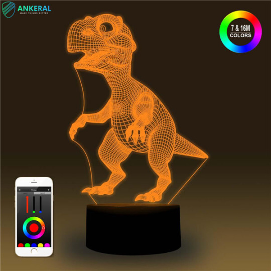
Illuminate Your Space with a Creative 3D LED Night Light – Unique Lamps for Every Room
Transform Your Space with a Creative 3D LED Night Light
When it comes to home decor and ambiance, lighting plays a crucial role. A creative 3D LED night light is not just a source of illumination—it’s a piece of art that enhances the aesthetic of any room. Whether you’re decorating your bedroom, a child’s nursery, or looking for a standout gift, 3D LED night lamps combine technology and creativity to deliver both function and flair.
In this blog, we’ll explore everything you need to know about 3D night lights, from how they work to the types of lamp bases available, and why they’ve become a favorite in modern home lighting.

What Is a 3D LED Night Light?
A 3D LED night light is a type of decorative lamp that uses optical illusion techniques and LED technology to create the appearance of a three-dimensional image or shape. These lamps often feature an acrylic panel etched with a design—like animals, anime characters, planets, or abstract art—that glows when inserted into the lamp base.
The result is a striking light effect that appears to “float” in 3D, despite being on a flat surface. Combined with energy-efficient LED bulbs and a wide variety of design choices, it’s easy to see why 3D night lights have grown in popularity.
Why Choose a Creative 3D Lamp?
If you’re looking for a unique and functional decor piece, a creative 3D lamp is the perfect solution. Unlike traditional table lamps or night lights, 3D LED lamps are:
Visually captivating – The illusion of depth creates a stunning 3D effect.
Customizable – Many brands offer the option to add names, messages, or personalized designs.
Energy-efficient – Using LED lights, these lamps consume minimal electricity.
Kid-friendly – Safe to touch, with no heat emissions, making them ideal for children’s rooms.
Stylish and modern – Sleek and minimal lamp bases fit into various interior styles.
Whether you’re gifting a loved one or refreshing your room decor, a creative 3D LED night light adds personality and warmth.

Ideal Use Cases for 3D LED Night Lamps
Here are some practical and imaginative ways to use a 3D LED night lamp in your home or office:
1. Bedroom Night Light
The soft glow of a 3D lamp creates a cozy, relaxing environment—perfect for winding down at night. It’s especially popular among kids and teens who want both lighting and a touch of personality in their space.
2. Children’s Nursery or Playroom
Choose animal-shaped or cartoon-inspired designs that appeal to young children. These lights provide comfort at night without being too bright or disruptive.
3. Gifts for All Occasions
A 3D night light makes a thoughtful gift for birthdays, anniversaries, baby showers, or even Valentine’s Day. With so many design options, you’re sure to find one that suits the recipient’s personality.
4. Home Office or Study Desk
Light up your workspace with something more inspiring than a plain lamp. Whether it’s a globe design or a motivational quote etched in 3D, it can add charm and focus to your desk.
5. Gaming or Media Rooms
Add visual excitement to your setup with LED lights that feature sci-fi, fantasy, or gaming-related themes. The ambient light adds depth and mood to your entertainment space.
Exploring the 3D Night LED Light Lamp Base
An important component of any 3D LED night lamp is the lamp base. The 3D night LED light lamp base is where the magic happens—it houses the LED bulbs and powers the optical illusion. There are several types of lamp bases available:
Single-color base: Emits one steady color (usually warm white or cool white).
Multi-color base: Offers several static colors and often comes with a touch or button control.
Remote-controlled base: Allows you to change colors, adjust brightness, or set flashing modes.
Rechargeable base: Ideal for portability and wireless placement.
USB-powered base: Plug into a power bank, laptop, or wall adapter for continuous use.
Look for a base that matches your lifestyle needs. For example, a rechargeable base is perfect for travel, while a remote-control version is better for bedrooms.
How to Choose the Best 3D Night Light for Your Home
Here are a few tips when selecting your ideal 3D illusion lamp:
Design matters: Choose a shape or design that resonates with the room’s theme or personal interests.
Light intensity: Make sure the brightness level suits the space. Soft lighting is better for sleeping areas.
Base features: Consider whether you need touch control, remote functions, or color-changing modes.
Size: Think about where you’ll place the lamp. Some are compact, while others are larger statement pieces.
Material quality: High-quality acrylic and LED chips ensure longevity and better illumination.
Benefits of Using 3D LED Night Lights
Aside from their stunning visuals, 3D LED lamps offer several advantages:
🌱 Energy Efficiency: LED bulbs use less energy and have a longer lifespan than traditional lighting.
🔒 Safety: No heat emission makes them safe for kids and pets.
🎨 Versatility: From romantic bedrooms to playful nurseries, there’s a 3D light for every room.
🎁 Gift-Ready: Beautifully packaged, many come gift-ready for holidays or special occasions.
Trending Designs in 3D LED Night Lamps
The world of 3D LED lights is incredibly diverse. Popular categories include:
🌌 Galaxy and space themes – Planets, astronauts, moon surfaces
🦄 Animals and nature – Unicorns, dinosaurs, birds, butterflies
🎮 Gaming and anime – Controllers, characters, manga figures
✍️ Custom text – Names, quotes, dates etched into the lamp
💕 Romantic designs – Hearts, couples, love messages
If you’re building a theme for your room or just want to express your personality, a creative 3D lamp can be the perfect accent.
Light Up Your Life with a 3D LED Night Lamp
A 3D LED night light is more than just a practical light source—it’s a mood setter, a conversation piece, and an artistic expression. Whether you’re decorating your home, shopping for a unique gift, or upgrading your workspace, there’s a 3D night light design to suit your needs.
With so many styles, features, and customization options, the only challenge is choosing your favorite.
0 notes
Text
Epoxy Coatings: The Ultimate Guide to Durable and Attractive Surface Protection
Epoxy coatings have rapidly become one of the most popular and effective solutions for protecting and beautifying surfaces across residential, commercial, and industrial environments. Whether you're upgrading a garage floor or sealing a warehouse, epoxy delivers unmatched durability, aesthetics, and longevity.
In this guide, we’ll cover everything you need to know about epoxy coatings, including benefits, types, applications, and tips for optimal installation. Plus, we’ll share how epoxy flooring can enhance your property's value while reducing maintenance costs.
What Are Epoxy Coatings?
Epoxy coatings are thermosetting resins that form when you mix a specific hardener with an epoxy polymer. Once applied to a surface, the mixture undergoes a chemical reaction that creates a rigid, plastic-like finish. The result is a strong, glossy surface that resists wear, chemicals, moisture, and heavy impacts.
Top Benefits of Epoxy Coatings
1. Exceptional Durability
Epoxy coatings are known for their ability to withstand heavy traffic, machinery, and harsh environmental conditions. This makes them ideal for warehouses, factories, garages, and even high-traffic commercial spaces.
2. Chemical and Stain Resistance
Epoxy is non-porous, which means it won’t absorb spills like oil, grease, or chemicals. This property makes cleaning a breeze and helps maintain a hygienic environment.
3. Enhanced Aesthetic Appeal
Available in a wide range of colors, patterns, and finishes (including metallic, flake, and matte), epoxy coatings can instantly transform a dull floor into a visually appealing space.
4. Long Lifespan
With proper preparation and application, epoxy floors can last 10 to 20 years or more, making them a cost-effective solution over time.
5. Eco-Friendly Options
Many epoxy systems are now formulated with low-VOC (volatile organic compounds) content, making them safer for indoor air quality and more environmentally responsible.
Common Applications of Epoxy Coatings
Residential Garages and Basements Epoxy flooring provides a clean, durable surface that's resistant to oil stains, water, and impact damage.
Commercial Kitchens and Hospitals Seamless and antimicrobial, epoxy is ideal for maintaining sanitary conditions.
Industrial Warehouses and Factories With resistance to forklifts, chemicals, and heat, epoxy floors handle tough environments effortlessly.
Retail Stores and Showrooms Aesthetic versatility and a glossy finish help enhance the customer experience.
Types of Epoxy Coatings
Self-Leveling Epoxy Great for old or uneven floors, providing a smooth, seamless finish.
Epoxy Mortar Systems Extremely durable—ideal for heavy-duty industrial applications.
Quartz-Filled Epoxy Combines epoxy resin with colored quartz for slip resistance and aesthetic appeal.
Anti-Static Epoxy (ESD) Prevents static discharge, perfect for sensitive electronic environments.
Metallic Epoxy Floors Offers a stunning, 3D-like finish—popular in showrooms and upscale interiors.
How to Apply Epoxy Coatings (DIY or Professional)
While epoxy kits are available for DIY use, professional installation is recommended for best results. Here's a quick overview of the process:
Surface Preparation: Clean, etch, or grind the surface to ensure proper adhesion.
Primer Application: Apply an epoxy primer to promote bonding.
Mixing Epoxy: Combine resin and hardener thoroughly.
Application: Roll or squeegee the epoxy evenly.
Curing Time: Allow at least 24–72 hours before use, depending on product specs.
These keywords help connect you with local professionals offering the specific services you need.
Final Thoughts
Epoxy coatings are a smart investment that adds both functionality and style to any space. Their resilience, low maintenance, and aesthetic versatility make them an increasingly popular choice across various industries.
If you're considering an upgrade to your floors, epoxy coating is a solution that delivers performance and value—year after year.
0 notes
Text
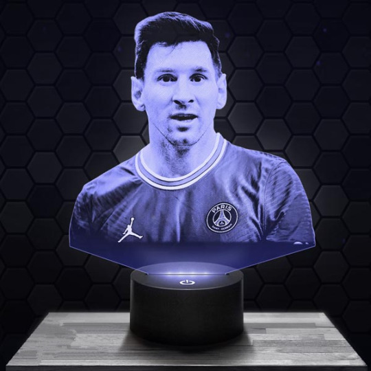
Custom 3D Crystal Engraving vs Traditional Engraving: What’s the Difference?
Discover the key differences between custom 3D crystal engraving and traditional engraving techniques. Learn why 3D crystal laser engraving services in UAE are the modern choice for timeless personalization.
In today’s world of personalized gifts and commemorative keepsakes, engraving has evolved beyond simple etching. Whether you’re celebrating a milestone, honoring a loved one, or promoting a brand, choosing the right engraving method is essential. Two popular options dominate the market: custom 3D crystal engraving and traditional engraving. But what sets them apart?
If you're exploring 3D crystal laser engraving services in UAE, understanding these differences will help you make an informed choice.
What Is Traditional Engraving?
Traditional engraving involves cutting or etching a design onto a physical surface—usually metal, wood, or glass—using tools like rotary machines, hand tools, or chemical processes. This technique has been around for centuries and is often used for plaques, trophies, nameplates, and jewelry.
Key Characteristics:
Surface-level engraving
2D designs or text only
Visible wear and tear over time
Limited detailing and depth
What Is Custom 3D Crystal Engraving?
Custom 3D crystal engraving uses advanced laser technology to embed 3D images, logos, or text inside a high-quality optical crystal without damaging the surface. This technique is highly precise and visually stunning, offering a floating 3D effect.
Key Characteristics:
Internal laser etching — no surface damage
3D imagery for depth and realism
Ideal for portraits, logos, awards, and keepsakes
Long-lasting and maintenance-free
3D Crystal Engraving vs Traditional Engraving: Key Differences
Feature
Traditional Engraving
3D Crystal Engraving
Method
Manual or mechanical surface etching
Laser-based internal engraving
Visual Effect
Flat, 2D
Realistic, floating 3D
Surface Impact
Leaves marks on surface
Surface remains intact
Durability
May wear over time
Highly durable and fade-resistant
Material Options
Wood, metal, plastic
Optical-grade crystal only
Detailing
Limited
Ultra-fine, lifelike precision
Why Choose 3D Crystal Laser Engraving Services in UAE?
The UAE is quickly becoming a hub for cutting-edge personalization and gifting trends. Here’s why 3D crystal laser engraving services in UAE stand out:
🌟 High-end gifting culture: Perfect for corporate awards, weddings, and VIP gifts.
🏢 Business-ready solutions: Ideal for branded keepsakes, corporate milestones, and promotional items.
🔍 Unmatched detail: Transform photos, logos, and 3D scans into crystal masterpieces.
💎 Luxury presentation: Each crystal comes polished and boxed, ready to impress.
Final Thoughts
While traditional engraving still holds its charm for rustic or metallic finishes, custom 3D crystal engraving offers unmatched sophistication, depth, and longevity. If you're looking for the next level in personalization or gifting, 3D crystal laser engraving services in UAE are the modern choice worth exploring.
Whether it’s for a personal gift or a professional gesture, the elegance of 3D engraved crystals will leave a lasting impression—literally and visually.
#3D Crystal Laser Engraving Services in UAE#Best 3D Crystal Laser Engraving Services in UAE#Top 3D Crystal Laser Engraving Services in UAE#Affordable 3D Crystal Laser Engraving Services in UAE#Engraving Services in UAE#Laser Engraving
0 notes
Text
Semiconductor Grade Solvents Market, Global Outlook and Forecast 2025-2032
The global Semiconductor Grade Solvents Market is experiencing robust expansion, reaching a valuation of USD 2.68 billion in 2024. Industry forecasts project sustained growth at a 7.0% CAGR, pushing market value to USD 4.27 billion by 2031. This trajectory reflects the critical role of ultra-pure solvents in semiconductor fabrication, where even parts-per-trillion impurities can disrupt advanced chip manufacturing processes.
Semiconductor grade solvents represent the backbone of chip production, enabling precise wafer cleaning, photoresist stripping, and surface preparation. Their application spans across semiconductor manufacturing, display technologies, and photovoltaic production, with purity requirements tightening as process nodes shrink below 3nm. The industry's shift toward EUV lithography and 3D NAND architectures is further elevating solvent performance benchmarks.
Download FREE Sample Report: https://www.24chemicalresearch.com/download-sample/291173/semiconductor-grade-solvents-forecast-market
Market Overview & Regional Analysis
Asia-Pacific dominates semiconductor solvent consumption, accounting for over 50% of global demand. This concentration stems from Taiwan's advanced foundries, South Korea's memory chip hubs, and China's rapidly expanding semiconductor ecosystem. The region benefits from close proximity to major chip manufacturers and government initiatives like China's "Big Fund" investments in domestic semiconductor capabilities.
North America maintains strong market presence through its leading-edge semiconductor research and manufacturing clusters, while Europe sees steady demand from specialized semiconductor applications. Emerging markets in Southeast Asia show promise as new semiconductor fabrication plants diversify global supply chains, creating localized solvent demand.
Key Market Drivers and Opportunities
The market's expansion rides on multiple technological and economic currents. The proliferation of 5G infrastructure demands high-frequency chips requiring ultra-clean surfaces, while automotive electrification increases semiconductor content per vehicle by 40% compared to traditional models. Meanwhile, AI hardware development pushes the boundaries of chip complexity, necessitating next-generation solvent formulations.
Opportunities abound in advanced packaging solutions like chiplet architectures and fan-out wafer-level packaging, where specialized solvents enable higher-density interconnects. The parallel growth of compound semiconductors for power electronics opens new application pathways, particularly for solvents compatible with gallium nitride and silicon carbide processing.
Challenges & Restraints
Market growth faces headwinds from increasing environmental regulations governing solvent emissions and waste treatment. The industry must balance purity requirements with sustainability goals as REACH and similar frameworks tighten VOC restrictions. Supply chain vulnerabilities also persist, with critical solvent precursors sometimes concentrated in geopolitically sensitive regions.
Technical challenges intensify as process nodes shrink—today's 2nm technologies demand solvent purity levels that were theoretical a decade ago. The capital intensity of purification infrastructure creates barriers for new entrants, while lengthy qualification processes slow supplier diversification in this stringent market.
Market Segmentation
By Product Type
Ultra High Purity Reagents
Functional Chemicals
By Application
Wafer Cleaning
Photolithography
Etching Processes
Packaging Applications
Competitive Landscape
The market features a mix of global chemical conglomerates and specialized purity solution providers:
Mitsubishi Chemical
Entegris (CMC Materials)
Stella Chemifa
Avantor
BASF
Honeywell
TOKYO OHKA KOGYO
JSR Corporation
Report Coverage
This comprehensive market analysis examines:
Technology trends in solvent purification and delivery systems
Purity standard evolution across semiconductor generations
Regional capacity expansions and supply chain dynamics
Strategic initiatives by leading market participants
Get Full Report Here: https://www.24chemicalresearch.com/reports/291173/semiconductor-grade-solvents-forecast-market
About 24chemicalresearch
Founded in 2015, 24chemicalresearch has rapidly established itself as a leader in chemical market intelligence, serving clients including over 30 Fortune 500 companies. We provide data-driven insights through rigorous research methodologies, addressing key industry factors such as government policy, emerging technologies, and competitive landscapes.
Plant-level capacity tracking
Real-time price monitoring
Techno-economic feasibility studies
With a dedicated team of researchers possessing over a decade of experience, we focus on delivering actionable, timely, and high-quality reports to help clients achieve their strategic goals. Our mission is to be the most trusted resource for market insights in the chemical and materials industries.
International: +1(332) 2424 294 | Asia: +91 9169162030
Website: https://www.24chemicalresearch.com/
Follow us on LinkedIn: https://www.linkedin.com/company/24chemicalresearch
0 notes
Text
3D Crystal Ball Lamp in Noida: A Perfect Blend of Art and Innovation
In the bustling city of Noida, where modernity meets tradition, home decor is a reflection of personal style and taste. One of the most sought-after decor pieces in recent years is the 3D Crystal Ball Lamp, a mesmerizing combination of light, art, and technology. Whether you are looking to enhance your home’s ambiance or searching for a perfect gift, these lamps offer a stunning visual experience.
What is a 3D Crystal Ball Lamp?
A 3D Crystal Ball Lamp is not just an ordinary light source; it is a piece of art. It consists of a crystal-clear spherical glass with intricate 3D engravings inside, which come to life when the lamp is lit. The 3D effect is created using laser engraving technology, which precisely etches the design within the glass without any damage to its surface. When illuminated, these designs glow beautifully, creating a captivating visual display.
Why Choose 3D Crystal Ball Lamps in Noida?
Noida, known for its vibrant lifestyle and modern architecture, is an ideal place to embrace the beauty of 3D Crystal Ball Lamps. Here are a few reasons why they are perfect for homes, offices, and even as gifts:
Modern Aesthetic: These lamps seamlessly blend with contemporary interiors, adding a touch of elegance.
Personalization: You can customize the 3D design, making it a thoughtful gift.
Energy-Efficient: LED lighting ensures low energy consumption and longevity.
Wide Range of Designs: From celestial patterns to personalized engravings, the options are endless.
Top 3D Crystal Ball Lamp Designs Available in Noida
Galaxy Design: A stunning view of the universe inside a crystal ball, perfect for stargazers.
Customized Portraits: Turn a cherished photo into a 3D crystal masterpiece.
Animal and Nature Themes: Perfect for nature lovers who wish to bring a touch of wildlife indoors.
Where to Buy 3D Crystal Ball Lamps in Noida?
Finding the perfect 3D Crystal Ball Lamp in Noida is now easier than ever. There are several reputed stores and online platforms where you can explore a wide variety of designs. Some of the best options include:
Local Gift Shops: Explore the markets in Sector 18 and Atta Market for unique and customized designs.
Online Stores: Websites like Kabira Gallery and other reputable online platforms offer a vast range of designs with doorstep delivery.
Shopping Malls: Visit popular malls in Noida like DLF Mall of India or Great India Place for premium collections.
How to Care for Your 3D Crystal Ball Lamp
To ensure that your 3D Crystal Ball Lamp remains as stunning as the day you bought it, follow these simple maintenance tips:
Keep It Clean: Use a soft, lint-free cloth to gently wipe the crystal surface.
Avoid Harsh Chemicals: Never use abrasive cleaners, which can damage the glass.
Safe Placement: Keep the lamp away from direct sunlight to prevent any discoloration.
3D Crystal Ball Lamps: The Perfect Gift Choice
Whether it’s a birthday, anniversary, or a special occasion, a 3D Crystal Ball Lamp can be a memorable and personalized gift. With the option to engrave a special image or message, it adds a personal touch that is sure to be cherished.
Conclusion: Elevate Your Space with 3D Crystal Ball Lamps in Noida
A 3D Crystal Ball Lamp in Noida is more than just a light source—it is an artistic creation that enhances the ambiance of any room. Whether you are decorating your home, setting up a cozy corner, or gifting someone special, these lamps offer a blend of style, sophistication, and personalization.
0 notes