#AXI4 DMA controller
Explore tagged Tumblr posts
Visit Tumblr Blog
Explore Tumblr blogs with no restrictions, modern design and the best experience.
Last Seen Tumblr Blogs


Fun Fact
After the announcement of the deal with Yahoo!, there were 170K signatures of unhappy Tumblr users petitioning to prevent the sale in 2013.
Text
Innovations in AHB DMA Controller for High-Speed Memory Access
In the rapidly evolving field of digital technology, efficient memory access remains a critical factor for system performance. At the heart of this challenge lies the AHB DMA controller, a key component designed to manage direct memory access with precision and speed. Digital Blocks has been at the forefront of innovating this technology, refining the AHB DMA controller to meet the demanding needs of modern applications.
Understanding the Role of the AHB DMA Controller
The AHB DMA controller plays a pivotal role in facilitating high-speed data transfers between memory and peripherals without burdening the central processing unit. By enabling direct memory access, this controller significantly reduces latency and frees up processing power for other critical tasks.
Digital Blocks has recognised the importance of this function and invested in enhancing the efficiency and reliability of the AHB DMA controller. These innovations allow for smoother data flow and improved system responsiveness, which are essential for industries relying on high-performance computing.
Enhancements in Data Transfer Efficiency
One of the significant advancements introduced by Digital Blocks in the AHB DMA controller involves optimising data transfer protocols. By improving how the controller manages burst transfers and prioritises data requests, the new designs achieve faster throughput rates.
This optimisation ensures that large blocks of data move seamlessly between system components, reducing bottlenecks that traditionally slow down operations. The result is a system that performs consistently at high speeds, meeting the rigorous standards of applications such as multimedia processing, communication devices, and embedded systems.
Robustness and Flexibility in Design
Digital Blocks’ approach to the AHB DMA controller also emphasises robustness and adaptability. The controller now supports multiple channel operations, allowing simultaneous data transfers without conflict. This multi-channel capability is crucial for systems that require parallel processing and multitasking.
In addition, the controller design offers configurability to match specific application requirements. This flexibility means that engineers can tailor the AHB DMA controller to optimise performance according to system needs. Such customisation ensures better power management and resource allocation, contributing to overall system efficiency.
Integration with Advanced System Architectures
The continuous development of the AHB DMA controller by Digital Blocks aligns well with the trends in system architecture. Modern designs increasingly demand controllers that integrate seamlessly with advanced bus systems and processors.
By maintaining compliance with industry standards and supporting a wide range of protocols, the AHB DMA controller fits into diverse system environments. This compatibility simplifies integration, reduces development time, and lowers costs. It also ensures that the controller remains relevant as new technologies emerge.
Conclusion: Leading the Future of Memory Access
The innovations introduced by Digital Blocks in the AHB DMA controller mark a significant step forward in high-speed memory access. By focusing on efficiency, robustness, and integration, these developments provide a reliable solution for today’s demanding digital systems.

As technology continues to advance, the need for powerful memory management tools will only grow. Digital Blocks’ commitment to refining the AHB DMA controller ensures that it remains a key player in supporting the future of high-performance computing.visit our website
#ahb dma controller#axi dma ip core#ahb dma verilog#axi4 stream dma#axi dma controller ip#axi dma scatter gather#axi bridge ip core#axi dma verilog#axi stream dma#axi4 data mover
0 notes
Text
Improving Design Productivity and Quality with Specification Automation

Designing semiconductor devices has always been a distinct specialty of engineering, but today’s designers face immeasurably greater challenges. A typical system-on-chip (SoC) design has billions of transistors, thousands of intellectual property (IP) blocks, hundreds of I/O channels, and dozens of embedded processors. Chip designers need all the help they can get.
Three Keys for Faster, Better Design
Assistance comes in three forms: abstraction, automation, and reuse. Virtually all chip design today occurs at the register transfer level (RTL), enabling much greater productivity than manually crafting gates or transistors. This level of abstraction is therefore much more efficient, making it possible for a single designer to create entire IP blocks or even subsystems.
RTL design is also amenable to automation; generating gate-level netlists automatically via logic synthesis is part of what makes the design process so efficient and productive. Just about every aspect of the test insertion, power management, layout, and signoff flow that follows RTL design is automated as well. Without this approach, modern SoCs simply would not be possible.
The third form of assistance is design reuse. Especially for standard IP blocks and interfaces, there is no value-add in reinventing the wheel by designing from scratch. EDA vendors and dedicated IP providers offer a huge range of reusable designs, most in RTL form. Designers often need this IP to be configurable and customizable, so it may come from a generator rather than as a fixed design.
Register Automation Is the Foundation
All three forms of designer assistance come together in specification automation, starting with the registers in the design. SoCs typically have a huge number of addressable (memory-mapped) registers defined by the chip specifications. These registers form the hardware-software interface (HSI) by which the embedded software and system drivers control the operation of the hardware.
Manually writing RTL code for all these registers is tedious and error-prone. Fortunately, the Agnisys IDesignSpec™ Suite makes it easy to automatically generate the register RTL design. Using the IDesignSpec GDI interactive tool or the IDS-Batch™ CLI Batch Tool, designers create their RTL files at the push of a button every time the register specification changes.
These tools accept many register and memory specification formats, including spreadsheets, SystemRDL, IP-XCAT, and the Portable Stimulus Standard (PSS). Designers can specify many widely used special register types, including indirect, indexed, read-only/write-only, alias, lock, shadow, FIFO, buffer, interrupt, counter, paged, virtual, external, and read/write pairs.

Registers are just one part of a chip that can be specified abstractly and generated automatically, fostering reuse and improving quality of results (QoR) with proven design IP. Another example is interfaces to standard buses such as APB, AHB, AHB-Lite, AXI4, AXI4-Lite, TileLink, Avalon, and Wishbone. The RTL design generated by IDesignSpec Suite includes any interfaces requested.
Any necessary clock-domain-crossing (CDC) logic across asynchronous clock boundaries is also included in the generated design. For safety-critical chip applications, designers can request that safety mechanisms such as parity, error-correcting code (ECC), cyclic redundancy check (CRC), and triple module redundancy (TMR) logic be included as well.
Most chips contain standard design elements such as AES, DMA, GPIO, I2C, I2S, PIC, PWM, SPI, Timer, and UART. Designers specify these blocks with many degrees of configuration and customization, and the Agnisys IDS-IPGen™ design tool generates the RTL design code. IDS-IPGen also generates finite state machines (FSMs) and other design elements for custom IP blocks.

Automating SoC Assembly
As noted earlier, SoCs contain thousands of standard and custom IP blocks. All of these must be connected together into the top-level chip design. Like register design, manually writing the RTL code for this stage is a tedious and error-prone process. Block inputs and outputs change many times over the course of a project, and updating the top-level RTL code by hand is extremely inefficient.
The Agnisys IDS-Integrate™ design tool, another part of the IDesignSpec Suite, automates the chip assembly process. Designers specify the desired hookup using a simple but powerful format that includes wildcards to handle buses and collections of signals with similar names. IDS-Integrate automatically generates the complete top-level RTL design.
For IP blocks with standard buses, IDS-Integrate automatically generates any required aggregators, bridges, and multiplexors, including them in the top-level RTL design. For example:
AHB interfaces on two IP blocks can be aggregated into a single bus
An AHB-to-APB bridge can connect IP using AHB and IP using APB

With the burden on SoC designers growing all the time, they need to specify at the highest possible level of abstraction, take advantage of automation, and reuse whenever possible. The specification automation capabilities of the Agnisys IDesignSpec Suite provide all three forms of designer assistance, providing the industry’s most complete solution.
Designers no longer have to hand-write RTL code for registers, memories, standard bus interfaces, aggregators, and bridges, CDC logic, safety mechanisms, custom IP elements, standard IP blocks, and top-level design. Abstract specification and automation improves productivity; reuse of proven IP improves quality of results.
Customization and configuration options ensure that designers do not have to sacrifice any flexibility to achieve these benefits. Many other project teams—verification, validation, embedded software, bringup, and documentation—also benefit from specification automation. The reasons to select Agnisys as a design partner are truly compelling.
0 notes
Text
"Accelerating System Performance with AXI4 Stream DMA, AXI Stream DMA, and eSPI IP Digital Blocks"
Digital blocks play a crucial role in modern electronic systems, providing essential functionality for communication, data transfer, and control. Among these blocks, the AXI4 Stream DMA, AXI Stream DMA, and eSPI IP are three critical components that enable efficient data transfer and communication between different modules in a system. In this blog, we will explore these digital blocks and their features, applications, and benefits.

AXI4 Stream DMA: The AXI4 Stream Direct Memory Access (DMA) is a digital block that facilitates high-speed data transfer between different modules in a system. It is a flexible and scalable interface that allows the transfer of large amounts of data between a source and a destination without involving the CPU. The AXI4 Stream DMA block is designed to be integrated into an AXI4-based system and supports a wide range of data transfer modes and burst sizes.
One of the main advantages of using the AXI4 Stream DMA block is its ability to offload data transfer tasks from the CPU, thereby reducing the workload on the processor and improving system performance. This makes it ideal for applications that require high-speed data transfer, such as video processing, audio processing, and network data transfer.
AXI Stream DMA: Similar to the AXI4 Stream DMA, the AXI Stream DMA is a digital block that provides a high-bandwidth, low-latency interface for data transfer in an AXI-based system. The AXI Stream DMA block is optimized for streaming data transfer and is ideal for applications that require real-time data transfer, such as audio and video processing, image processing, and machine learning.
One of the key features of the AXI Stream DMA block is its support for multiple channels, which enables simultaneous data transfer between different modules in a system. This feature makes it ideal for applications that require parallel data transfer, such as multi-camera video processing and multi-channel audio processing.
eSPI IP: The Enhanced Serial Peripheral Interface (eSPI) is a digital block that provides a high-speed, low-latency interface for communication between different modules in a system. The eSPI IP block is designed to replace the legacy Low Pin Count (LPC) interface and improve system performance by providing faster data transfer rates, higher bandwidth, and improved scalability.
One of the key features of the eSPI IP block is its support for multiple devices, which enables communication between different modules in a system, such as the CPU, chipset, and peripherals. This feature makes it ideal for applications that require efficient communication between multiple devices, such as server systems, high-performance computing systems, and embedded systems.
In conclusion, the AXI4 Stream DMA, AXI Stream DMA, and eSPI IP are three critical digital blocks that enable efficient data transfer and communication between different modules in a system. These blocks are designed to improve system performance, reduce CPU workload, and enable real-time data transfer and communication. As digital systems continue to evolve, these blocks will play an increasingly important role in enabling faster, more efficient, and more scalable systems.
0 notes
Text
PCIe 4.0 PHY IP Cores in 7nm for reliable Low area High Speed Interface Peripheral
T2MIP, the global independent semiconductor IP Cores provider & Technology experts, is pleased to announce the immediate availability of its partner’s PCI-SIG compliant PCIe 4.0 PHY IP Cores Silicon Proven in 7nm process technology with matching PCIe 4.0 Controller IP cores. This PCIe Cores have been in use in several different chipsets and applications.
The high-bandwidth applications benefit from the low power, multi-lane, and high-performance PCIe 4.0 PHY IP's design. A full variety of PCIe 4.0 Base applications are supported by the PCIe 4.0 IP cores, which also complies with the PIPE 4.4.1 specification. The IP cores integrates high-speed mixed signal circuits to support PCIe 4.0 traffic at 16Gbps. This Silicon Proven 7nm technology boasts a Low power consumption, achieved due to support of additional PLL control, reference clock control, embedded power gating control and support for all power saving modes (P0, P0s, P1, P2) defined in PIPE4.4.1 spec.
The PCIe 4.0 SerDes PHY IP cores supports data transfer rates of 16Gbps and is backward compatible with data rates of 2.5Gbps, 5.0Gbps, and 8.0Gbps for PCIe 3.1, PCIe 2.1, and PCIe 1.1, respectively. The PCIe 4.0 IP cores may satisfy the needs for various channel circumstances since it supports both TX and RX equalisation method along with a x4 width physical lane which can also support x1, x2, x4, x8, x16 lane configurations with bifurcation. Parallel interface of 32-bit is supported with an input reference clock of 100 MHz. It can also support parallel interface data clock of 62.5 MHz, 125 MHz and 250 MHz and 500MHz.
The PCIe 4.0 Controller IP cores presents a programmable, flexible AMBA AXI connection interface to the user and may be configured to support endpoint, root port, and dual-mode topologies, allowing for a range of use cases. For extremely high performance, it has a 512b Controller architecture and 64B PIPE interface. AXI4/Native Interfaces and a highly programmable, reliable DMA architecture guarantee a versatile user interface and an effective gate controller.

As the industry standard for PCI Express, PCIe 4.0 PHY IP Cores in 7nm which T2M offers is in volume production and has been successfully implemented in a wide range of applications such as SSD Controller, Digital TV, Setup Box, Desktops, workstations, servers, Automotive, Embedded systems, Network switches, and Enterprise computing…
In addition to PCIe IP Cores, T2M ‘s broad silicon Interface IP Core Portfolio includes USB, HDMI, Display Port, MIPI (CSI, UniPro, UFS, RFFE, I3C), PCIe, DDR, 1G Ethernet, V-by-One, programmable SerDes, OnFi and many more, available in major Fabs in process geometries as small as 7nm. They can also be ported to other foundries and leading-edge processes nodes on request.
Availability: These Semiconductor Interface IP Cores are available for immediate licensing either stand alone or with pre-integrated Controllers and PHYs. For more information on licensing options and pricing please drop a request / MailTo
About T2M: T2MIP is the global independent semiconductor technology experts, supplying complex semiconductor IP Cores, Software, KGD and disruptive technologies enabling accelerated development of your Wearables, IOT, Communications, Storage, Servers, Networking, TV, STB and Satellite SoCs. For more information, please visit: www.t-2-m.com
1 note
·
View note
Text
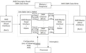
AXI DMA Controller IP Cores

Beginning direct memory access with digital blocks is quite amazing. The AXI DMA Controller IP gives high-data transfer capacity direct memory access amongst memory and AXI4-Stream-type target peripherals. Its discretionary disperse accumulate capacities additionally offload information development undertakings from the Central Processing Unit in processor based frameworks. We offer 1-16 Channels for every channel CPU descriptor-driven interface controlling the information exchange between memory subsystems or amongst memory and a peripheral. The AXI DMA Controller highlights Scatter-Gather capacity, with per channel Finite State Control and single-or double check FIFOs parameterized top to bottom and width, interfere with controller, and discretionary information equality generator and checker. The AXI Master Data Interface scales from 32-to 256-bits, with programmable information blasts of 1, 4, 8, 16 words with the little information exchange bolstered is 1 byte, and up to 16 exceptional read demands, and for AXI4, the accessibility of programmable Quos and longer information burst lengths. The AXI DMA Controller additionally gives an APB or AXI-lite Slave Interface for CPU access to Control Status Registers. The DB-DMAC-MC-AXI is tuned as elite DMA Engine, for huge and little data blocks transfers. Digital Blocks DMA Controller IP Cores offer an adaptable CPU programming interface and superior exchange rates with driving AMBA Interconnects and standard or redid fringe interfaces. Our DMA Controllers are rich with Multi-Channel, Axi Dma Scatter Gather ability with IP discharges focusing on CPU AXI/AHB spine DMA Engines, PCI Express DMA, and Peripheral high or low information rate DMA exchanges. Reach us today to get more news @ https://www.digitalblocks.com/dma.html.
0 notes
Text
#ahb dma controller#axi dma ip core#axi dma scatter gather#axi bridge ip core#axi dma verilog#axi dma controller ip#axi stream dma#ahb dma verilog#axi4 stream dma#axi4 data mover
0 notes
Text
#ahb dma controller#axi dma scatter gather#axi dma ip core#axi bridge ip core#axi dma verilog#ahb dma verilog#axi dma controller ip#axi4 data mover#axi stream dma#axi4 stream dma
0 notes
Text
Reducing Latency in Real-Time Applications with AXI4 Stream DMA
In real-time systems, every microsecond counts. Industries like telecommunications, automotive, medical, and defense demand instant data movement between processing units. Any delay can affect performance, accuracy, or safety. Digital Blocks, through its advanced design of AXI4 Stream DMA, is addressing this demand with precision and efficiency.
The Need for High-Speed Data Transfer
Real-time applications depend on the continuous and rapid flow of data. Tasks such as video processing, sensor fusion, and control systems require minimal delay between data capture and action. Standard memory-mapped data transfers often introduce latency due to handshaking, memory access, and software intervention. This slows down systems that must respond without delay.
The AXI4 Stream DMA developed by Digital Blocks helps bypass these barriers. It supports direct data transfers between sources and destinations with minimal CPU involvement. This makes it ideal for applications that require predictable and fast performance.
How AXI4 Stream DMA Improves System Speed
The AXI4 Stream DMA core is built to handle large volumes of data at high speed. It supports streaming data interfaces, where information is transferred in a continuous flow. This design reduces the overhead of individual memory transactions and avoids congestion that slows down traditional DMA systems.
By handling data transfers autonomously, the AXI4 Stream DMA allows the processor to focus on higher-level tasks. Digital Blocks has designed this module to be both lightweight and powerful, ensuring it fits into a wide range of system-on-chip (SoC) designs without consuming unnecessary resources.
Scalability for Complex Applications
Real-time systems vary in size and function. Some may require small and frequent data packets, while others need high-bandwidth continuous streaming. Digital Blocks addresses this need through a scalable AXI4 Stream DMA solution. It supports configurable parameters to match system architecture and data flow requirements.
Developers working on multi-core designs or FPGA-based systems can integrate AXI4 Stream DMA to improve performance while keeping latency under control. The design supports burst transfers, flow control, and error detection, all key features that enhance reliability.
Proven in Real-World Applications
Digital Blocks has delivered its AXI4 Stream DMA core to customers across multiple sectors. In each case, the goal was clear: reduce latency and improve data throughput without compromising system stability. Applications such as real-time video encoding, radar signal processing, and industrial automation have shown marked improvements after adopting this design.
By focusing on a robust, standards-based solution, Digital Blocks ensures that the AXI4 Stream DMA integrates smoothly with existing AXI-based systems. This reduces the time and cost of development while improving end-product performance.
Building the Future of Low-Latency Systems
Latency will always be a concern in real-time systems. However, the right architecture can bring it within acceptable limits. The AXI4 Stream DMA by Digital Blocks provides a focused solution to this challenge. With careful design and proven efficiency, it supports the fast, consistent data flow that modern systems demand.
As real-time applications continue to grow in complexity, Digital Blocks remains committed to delivering high-performance solutions that keep pace with future needs. More details visit us
#ahb dma controller#axi4 stream dma#axi bridge ip core#axi dma controller ip#ahb dma verilog#axi dma scatter gather#axi dma ip core#axi dma verilog#axi4 data mover#axi stream dma
0 notes
Text
#ahb dma controller#axi dma scatter gather#ahb dma verilog#axi dma ip core#axi dma controller ip#axi dma verilog#axi stream dma#axi bridge ip core#axi4 stream dma#axi4 data mover
0 notes
Text
AXI DMA Scatter Gather Enhancing Real-Time Data Streaming in SoC Designs
In today’s high-performance SoC designs, real-time data movement plays a critical role. Applications in communications, video processing, and AI demand reliable and efficient data streaming. To support these demands, AXI DMA Scatter Gather has become a powerful tool. At the forefront of this advancement stands Digital Blocks, delivering IP solutions that streamline data flow with precision and speed.

Meeting High-Speed Data Requirements
System-on-Chip designs today face increasing pressure to handle complex workloads with minimal latency. Traditional DMA approaches often fall short in scenarios where data sources and destinations are fragmented. AXI DMA Scatter Gather addresses this problem by allowing data transfers across non-contiguous memory regions without software intervention for each block.
Digital Blocks provides AXI DMA Scatter Gather IP that ensures consistent data flow in real-time systems. This approach helps manage bandwidth and reduces CPU load, which is critical in time-sensitive applications. With fewer interrupts and lower processing overhead, system responsiveness improves across all operations.
Smart Buffer Management
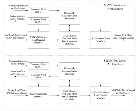
The AXI DMA Scatter Gather model enables intelligent buffer management. It uses a descriptor-based mechanism to define memory segments. Each descriptor holds address, length, and control data for a segment. The DMA engine reads these descriptors and processes them autonomously.
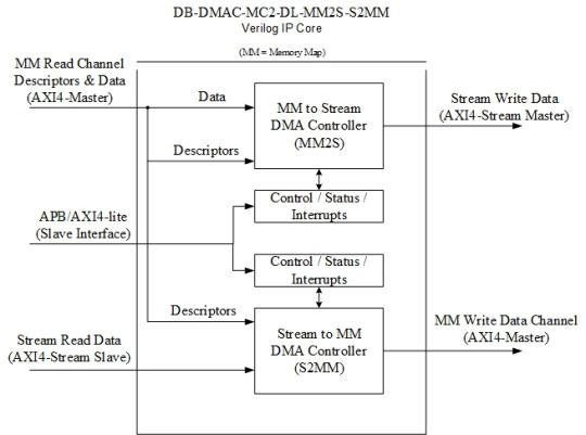
Digital Blocks integrates this structure with a focus on flexibility and stability. Their IP handles both memory-to-stream and stream-to-memory directions efficiently. It supports continuous and burst transfers with minimal CPU involvement. This results in streamlined operations that are ideal for multi-channel or multi-core systems.
Supporting Advanced Use Cases
Applications like 4K video processing, machine learning, and software-defined radio benefit directly from AXI DMA Scatter Gather. These use cases require large amounts of data to be moved quickly and reliably. Any delay can disrupt system behavior or cause quality issues.
Digital Blocks designs their AXI DMA Scatter Gather IP to match such requirements. It supports programmable burst sizes, interrupt coalescing, and address alignment. This ensures that the IP adapts to system needs without placing stress on core resources. In environments where data integrity and speed matter, this feature set makes a measurable difference.
Seamless SoC Integration
Another strength of Digital Blocks' solution lies in its ease of integration. The AXI interface enables smooth connection with standard bus architectures used in SoC designs. The IP core works with AXI4 and AXI4-Stream protocols, allowing wide compatibility across platforms.
Digital Blocks supports engineers through every phase of implementation. Their design ensures scalability, making it suitable for both low-power embedded designs and high-throughput computing systems. It helps reduce development time and allows design teams to focus on application-level innovation.
Driving Innovation in Real-Time Systems
AXI DMA Scatter Gather by Digital Blocks is helping shape the future of real-time data streaming in SoCs. Its efficient use of system memory, reduced CPU intervention, and high-speed performance make it a valuable asset in advanced designs.
By focusing on reliability and intelligent data handling, Digital Blocks continues to deliver IP that meets today’s performance challenges and prepares systems for tomorrow’s demands. For more details visit us
#ahb dma controller#axi dma ip core#axi dma controller ip#axi stream dma#axi bridge ip core#ahb dma verilog#axi dma scatter gather#axi4 data mover#axi dma verilog#axi4 stream dma
0 notes
Text

The AXI DMA Controller IP is a digital block used in FPGA designs to transfer data between memory and AXI-compatible peripherals without CPU intervention, enabling high-speed, efficient data movement using Direct Memory Access (DMA).
#ahb dma controller#axi dma ip core#axi dma scatter gather#ahb dma verilog#axi dma verilog#axi dma controller ip#axi bridge ip core#ahb dma ip verilog#axi stream dma#axi4 stream dma#axi4 data mover
0 notes
Text

Digital Blocks offers high-performance AXI Bridge IP Core solutions, enabling seamless data transfer and protocol conversion for FPGA and ASIC designs. Our AXI bridges ensure efficient communication between AXI-based systems, supporting AXI-to-AHB, AXI-to-APB, and AXI-to-PCIe interfaces with low latency and high throughput. Designed for scalability and customization, our IP cores optimize embedded systems, high-performance computing, and SoC architectures. For More Details Visit Us.
#ahb dma controller#axi dma scatter gather#axi dma ip core#axi stream dma#axi4 stream dma#ahb dma verilog
0 notes
Text
Enhancing High-Speed Data Transfers with AXI DMA Scatter-Gather: A Complete Guide!
Efficient data movement is crucial in high-performance computing and embedded systems. AXI DMA Scatter-Gather plays a vital role in optimizing high-speed data transfers, reducing CPU workload, and enhancing overall system efficiency. In this guide, we will explore the fundamentals of AXI DMA Scatter-Gather, its advantages, and how Digital Blocks provides industry-leading solutions to meet your design needs.
Understanding AXI DMA Scatter-Gather
AXI DMA Scatter-Gather is an advanced Direct Memory Access (DMA) technique that enables efficient data transfer across multiple memory locations. Unlike traditional DMA, which moves data in fixed blocks, scatter-gather mode allows data to be transferred dynamically, improving system flexibility and performance.

Key Benefits of AXI DMA Scatter-Gather:
Reduced CPU Overhead: By offloading data movement tasks, it frees up CPU resources for other critical operations.
Increased Data Transfer Efficiency: It minimizes memory fragmentation and optimizes data throughput.
Low-Latency Performance: Ideal for real-time applications requiring high-speed data processing.
Scalability: Supports high-bandwidth applications in networking, video processing, and AI/ML systems.
How AXI DMA Scatter-Gather Works
The Scatter-Gather mechanism in AXI DMA utilizes a descriptor-based architecture, where each descriptor defines the source, destination, and transfer parameters. This enables seamless handling of multiple data chunks without CPU intervention.
The Process Includes:
Descriptor Preparation: The CPU prepares a linked list of descriptors for data movement.
DMA Controller Execution: The AXI DMA engine reads the descriptors and executes transfers autonomously.
Completion Notification: The system receives an interrupt when the transfer is complete, ensuring seamless data flow.
Digital Blocks: Leading the Way in AXI DMA Scatter-Gather Solutions
At Digital Blocks, we specialize in providing silicon-proven AXI DMA Scatter-Gather IP cores designed to enhance the performance of your FPGA, ASIC, and SoC designs. Our high-performance DMA controllers enable efficient, low-latency data movement, making them ideal for applications in networking, automotive, video processing, and artificial intelligence.
Why Choose Digital Blocks?
Proven Expertise: Over two decades of experience in developing high-speed IP cores.
Optimized Performance: Designed for high-throughput, low-latency applications.
Seamless Integration: Fully compatible with industry-standard AXI architectures.
Customizable Solutions: Tailored to meet specific project requirements.
Conclusion
AXI DMA Scatter-Gather is a game-changer in high-speed data transfers, enabling efficient memory management and reducing CPU workload. With Digital Blocks' industry-leading AXI DMA solutions, engineers can accelerate their designs, improve system performance, and achieve faster time-to-market. For More Details:- https://www.digitalblocks.com/axi-dma-verilog-ip-core/
0 notes
Text
axi4 stream dma
Elevate your system's data handling capabilities with our cutting-edge Digital Blocks AXI4 Stream DMA controller. Engineered for efficiency and speed, this module facilitates seamless data transfers between various peripherals and memory units. Incorporating the latest AXI4 protocol standards, this DMA controller ensures smooth and reliable data transmission for various applications. Visit Us https://www.digitalblocks.com/dma-verilog-ip-cores/
0 notes
Text
AXI DMA IP Core: Optimizing High-Performance Data Transfers in FPGA Systems
In FPGA (Field-Programmable Gate Array) systems, efficient data transfer is crucial for optimal performance. The AXI DMA IP Core (Advanced eXtensible Interface Direct Memory Access Intellectual Property Core) plays a vital role in facilitating high-speed data movement between memory and peripherals, minimizing CPU involvement and enhancing overall system efficiency.
Understanding AXI DMA IP Core
The AXI DMA IP Core is designed to handle direct memory access operations within FPGA architectures. It enables peripherals to directly read from or write to memory without continuous CPU intervention, thereby reducing latency and freeing up processor resources for other tasks.

Key Features of AXI DMA IP Core
High Throughput: Supports data widths ranging from 32 to 1024 bits, allowing for rapid data transfers suitable for both small and large datasets.
Scatter-Gather Capability: Utilizes scatter-gather lists to manage data transfers efficiently, supporting various transfer scenarios such as memory-to-memory, peripheral-to-memory, and peripheral-to-peripheral.
Flexible Configuration: Offers a configurable number of channels (from 1 to 16), each with independent read and write controllers, enabling tailored solutions for specific application requirements.
Compliance with AMBA Standards: Fully compliant with AMBA AXI4 and AXI3 interconnects, ensuring seamless integration into existing FPGA designs.
Digital Blocks' AXI DMA IP Core Solutions
At Digital Blocks, we specialize in providing high-quality AXI DMA IP Core solutions tailored to meet the diverse needs of FPGA system designers. Our offerings include:
Multi-Channel Support: Our AXI DMA Controllers support 1 to 16 independent data transfer channels, each with scatter-gather capabilities, ensuring efficient data movement across various system components.
High-Performance Design: Optimized for both small and large data sets, our DMA controllers excel in delivering high data throughput, crucial for applications requiring rapid data processing.
Comprehensive Integration: Fully compliant with AMBA AXI4 and AXI3 interconnects, our IP cores integrate seamlessly into existing FPGA designs, facilitating smooth system development and deployment.
Customizable Features: We offer flexible configurations, allowing designers to tailor the DMA controller's features to specific application requirements, ensuring optimal performance and resource utilization.
Conclusion
Implementing an AXI DMA IP Core is essential for optimizing high-performance data transfers in FPGA systems. By offloading data movement tasks from the CPU, it enhances system efficiency, reduces latency, and improves overall performance. Digital Blocks is committed to providing robust and flexible AXI DMA IP Core solutions, empowering designers to achieve their performance goals in various FPGA applications. For More Details:- https://www.digitalblocks.com/?utm_source=SEO&utm_medium=SEO&utm_campaign=blog
0 notes
Text
AXI DMA Scatter Gather – What You Need to Know
AXI DMA scatter-gather is a powerful function that allows you to move data between different memory locations in a quick and efficient manner. In this blog post, we will discuss what scatter-gather is and what you need to know about it.

What is AXI DMA scatter-gather?
AXI DMA scatter-gather is a feature that allows a device to send data to multiple memory addresses in a single DMA transaction. This can improve performance by reducing the number of transactions required to send data to multiple destinations.
What are the benefits of using scatter-gather?
There are many benefits to using scatter-gather.
● it allows you to process data more efficiently.
● With scatter-gather, you can process data that is spread out across a network more quickly and easily this makes it a great choice for applications that require a lot of data processing.
● Another benefit of scatter-gather is that it can help improve performance. When data is scattered across a network, it can be accessed more quickly than if it was all stored in one place. This can help improve the performance of applications that rely on data access.
● scatter-gather can also help improve security. When data is scattered across a network, it is more difficult for hackers to access it all at once. This can help keep your data safe from unauthorized access.
How do you use scatter gather?
AXI DMA scatter-gather is a powerful tool that can be used for a variety of purposes.
● In its most basic form, scatter-gather allows you to quickly and easily gather data from multiple sources and combine it into a single dataset. This can be useful for data analysis and reporting, or for creating customizations and extensions for Dynamics 365.
● AXI DMA scatter-gather can also be used to create dynamic lists. This can be useful for creating lists of records that are filtered and sorted based on the user's selections. For example, you could create a list of customers that are located in a specific city, or a list of products that are on sale this week.
● scatter-gather can be used to create lookup tables. This can be useful for creating tables of data that are used to look up information in other tables. For example, you could create a table of states, and then use that table to look up the postal code for a specific state.
#axi dma scatter gather#axi4 dma#axi dma controller#AXI4 DMA controller#Display Controller IP#display controller#LCD Controller IP#I2C controller ip#i2C Master IP#I2C Slave IP#i3C Basic IP#I3C controller ip#i3c master#i3c slave#i3c basic
0 notes