#Epoxy Encapsulation for Electrical Material
Explore tagged Tumblr posts
Visit Tumblr Blog
Explore Tumblr blogs with no restrictions, modern design and the best experience.
Last Seen Tumblr Blogs


Fun Fact
Users from the US are the majority of Tumblr visitors.
Text
Epoxy Encapsulation for Superior Durability
Looking for advanced epoxy encapsulation solutions? MB Enterprises provides high-quality epoxy resin, ideal for protecting electrical components and materials from environmental factors. Our resins are engineered for superior durability and reliable performance, making them the preferred choice for industries requiring precision encapsulation.
With MB Enterprises, experience the benefits of epoxy encapsulation designed to meet industrial standards. Partner with us to ensure your projects are secure and long-lasting with cutting-edge epoxy solutions tailored to your needs.

#Epoxy Encapsulation#Epoxy for Encapsulation#Epoxy Encapsulation for Electrical Material#Advanced Resin Material
0 notes
Text
Glass-encapsulated NTC Thermistor Market: Forecasting Future Developments to 2025-2032

MARKET INSIGHTS
The global Glass-encapsulated NTC Thermistor Market size was valued at US$ 389.5 million in 2024 and is projected to reach US$ 678.9 million by 2032, at a CAGR of 8.34% during the forecast period 2025-2032. The U.S. market accounted for 28% of global revenue in 2024, while China’s market is expected to grow at a faster CAGR of 6.7% through 2032.
Glass-encapsulated NTC thermistors are precision temperature sensors featuring a negative temperature coefficient (NTC) element hermetically sealed in glass. This encapsulation provides superior environmental protection against moisture, chemicals, and mechanical stress compared to polymer-coated alternatives. These components are critical for temperature measurement and compensation in demanding applications across industries.
The market growth is driven by increasing adoption in medical devices, automotive systems, and industrial automation where reliability under harsh conditions is paramount. Recent advancements include miniaturized designs for wearable medical devices and high-temperature variants for electric vehicle battery management. Key players like Mitsubishi Materials and Vishay are expanding production capacities to meet rising demand, particularly in Asia-Pacific markets where electronics manufacturing is concentrated.
MARKET DYNAMICS
MARKET DRIVERS
Expanding Applications in Medical Devices to Accelerate Market Growth
The medical industry’s increasing adoption of glass-encapsulated NTC thermistors is creating significant growth opportunities. These components are critical in patient monitoring equipment, diagnostic devices, and therapeutic applications due to their high stability and accuracy. Over 65% of new medical devices requiring temperature sensing now incorporate glass-encapsulated variants rather than epoxy alternatives. The global medical sensors market, valued at over $25 billion in 2024, is projected to maintain a steady 7-9% CAGR through 2032, directly benefiting NTC thermistor manufacturers. Recent FDA approvals for smart medical implants with integrated temperature monitoring are further driving demand for reliable sensor solutions.
Automotive Electrification Trends to Fuel Demand
The automotive industry’s transition toward electric vehicles represents a major growth driver for glass-encapsulated NTC thermistors. These components are essential for battery thermal management systems in EVs, with each vehicle containing 15-25 thermistors on average. With global EV production expected to surpass 40 million units annually by 2030, demand for temperature sensors is projected to increase proportionally. Glass encapsulation provides the necessary durability against vibration and harsh under-hood conditions while maintaining measurement precision within ±0.5°C. Leading automakers are increasingly specifying glass-encapsulated versions for critical applications after demonstrating superior performance in accelerated life testing.
Industrial Automation Investments Driving Market Expansion
As Industry 4.0 initiatives gain momentum, glass-encapsulated NTC thermistors are becoming integral components in smart factories. Their ability to withstand industrial environments while providing reliable temperature data makes them ideal for predictive maintenance systems and process control applications. Manufacturing facilities are allocating over 30% of their sensor budgets to ruggedized temperature measurement solutions. The glass encapsulation provides chemical resistance critical for food processing, pharmaceutical production, and chemical manufacturing applications where epoxy alternatives would degrade. This sector alone accounts for nearly 40% of current glass-encapsulated NTC thermistor demand.
MARKET RESTRAINTS
Higher Production Costs Limiting Price-Sensitive Applications
While glass-encapsulated NTC thermistors offer superior performance, their manufacturing costs remain approximately 35-45% higher than standard epoxy-encapsulated alternatives. This price differential makes them less competitive in consumer electronics and other cost-sensitive markets where slight reductions in accuracy are tolerable. The specialized glass sealing process requires controlled atmosphere furnaces and precision handling equipment, contributing to elevated capital expenditures for manufacturers. In industries where hundreds of thousands of units are deployed annually, these cost considerations significantly impact purchasing decisions despite the technical advantages.
Complex Manufacturing Processes Affecting Supply Chain Dynamics
The production of glass-encapsulated NTC thermistors involves multiple precise steps including glass formulation, hermetic sealing, and rigorous testing. Each batch requires strict environmental controls throughout the manufacturing process. These complexities have resulted in longer supplier lead times averaging 12-16 weeks compared to 4-6 weeks for standard thermistors. The supply chain bottlenecks became particularly evident during recent semiconductor shortages, with some automotive manufacturers reporting 20-30% delays in sensor deliveries. This manufacturing intricacy also limits the number of qualified suppliers globally, reducing buyer flexibility.
MARKET CHALLENGES
Miniaturization Requirements Pushing Technical Boundaries
As end-use devices continue shrinking, thermistor manufacturers face mounting pressure to reduce package sizes while maintaining performance standards. Developing glass-encapsulated versions below 0.8mm diameter presents significant technical hurdles in hermetic sealing reliability. Current yields for sub-miniature glass packages remain below 60% in production environments compared to over 85% for standard sizes. This challenge is particularly acute in medical applications where device makers demand sensors smaller than 0.5mm for minimally invasive instruments. The industry must overcome material science limitations to achieve both miniaturization and durability targets.
Standardization Gaps Creating Interoperability Issues
The absence of universal standards for glass formulations and encapsulation methods is creating compatibility challenges across the supply chain. Different manufacturers utilize proprietary glass compositions with varying coefficients of thermal expansion, leading to performance inconsistencies in critical applications. These variations complicate system integration and require extensive requalification when changing suppliers. Industry groups are beginning to address these issues, but progress toward standardization has been slow despite growing recognition of the need.
MARKET OPPORTUNITIES
Emerging Battery Storage Applications Offering New Growth Prospects
The rapid expansion of grid-scale battery storage systems presents a significant opportunity for glass-encapsulated NTC thermistor suppliers. These installations require robust temperature monitoring solutions capable of withstanding 20+ year operational lifetimes in harsh environments. Recent pilot projects have demonstrated glass-encapsulated variants delivering 99.9% reliability over 5,000 thermal cycles—performance unmatched by alternative technologies. With global energy storage capacity projected to increase sixfold by 2030, this application could comprise 15-20% of total market demand within the next decade.
Advancements in Wireless Sensor Networks Creating Ecosystem Opportunities
The integration of glass-encapsulated NTC thermistors with energy-harvesting wireless nodes is enabling new monitoring applications in previously inaccessible environments. Recent developments in low-power sensor ICs allow operation for years without battery replacement when paired with these reliable temperature elements. Industrial facilities are deploying these solutions for equipment health monitoring, with adoption rates increasing approximately 40% annually. Suppliers offering pre-engineered wireless sensor modules are capturing significant market share by reducing implementation barriers for end-users.
GLASS-ENCAPSULATED NTC THERMISTOR MARKET TRENDS
Expanding Industrial Applications Drive Market Demand
The global glass-encapsulated NTC thermistor market is witnessing robust growth, primarily fueled by increasing adoption across industrial applications. These thermistors offer superior performance in harsh environments due to their hermetic glass encapsulation, which protects against moisture and chemical exposure. Industries such as automotive, aerospace, and manufacturing rely heavily on these components for precise temperature monitoring in critical systems. The automotive sector alone accounts for over 30% of global demand, with electric vehicle production accelerating adoption further. Additionally, glass-encapsulated thermistors are becoming indispensable in industrial automation, where sensor reliability directly impacts operational efficiency. With industrial IoT deployments growing at 15% annually, the need for durable, high-precision temperature sensors continues to rise.
Other Trends
Medical Technology Advancements
Medical applications are emerging as a significant growth segment for glass-encapsulated NTC thermistors. Their small form factor and biocompatibility make them ideal for invasive medical devices and diagnostic equipment. The global medical sensors market, valued at $16 billion in 2024, is projected to incorporate increasingly sophisticated temperature monitoring solutions. With minimally invasive surgeries growing by 8% annually, demand for tiny yet reliable thermistors in catheters and endoscopic tools is surging. Furthermore, wearable health monitors and implantable devices are adopting these sensors for continuous temperature tracking, creating new revenue streams for manufacturers.
Miniaturization and Material Innovations
Technological advancements in material science and manufacturing processes are enabling the production of smaller, more efficient glass-encapsulated NTC thermistors. The trend toward miniaturization is particularly evident in consumer electronics, where component space is at a premium. Smartphone manufacturers now incorporate these thermistors for battery temperature management in devices that generate significant heat during fast charging. Meanwhile, new glass compositions with enhanced thermal conductivity and durability are extending sensor lifespans in extreme conditions. These innovations are driving replacement cycles in industrial settings, where sensor failure can lead to costly downtime. With over 40% of industrial equipment failures relating to temperature issues, the reliability benefits of advanced glass-encapsulated thermistors justify their premium pricing in critical applications.
COMPETITIVE LANDSCAPE
Key Industry Players
Companies Invest in Innovation and Regional Expansion for Market Dominance
The global Glass-encapsulated NTC Thermistor market is moderately fragmented, with established manufacturers and emerging regional players competing for market share. WEILIAN leads the market with its comprehensive product range and strong foothold in Asia-Pacific, particularly in industrial applications where precision temperature sensing is critical. Their revenue share in 2024 reflects their technological edge in high-stability thermistor solutions.
Chinese manufacturers like Shenzhen Minchuang Electronics Co., Ltd. and Sinochip Electronics C0., LTD have gained significant traction, leveraging cost-effective production capabilities and rapid response to regional demand. These companies now collectively account for nearly 30% of the Asia-Pacific market, challenging traditional Western suppliers.
Meanwhile, Japanese firms such as Mitsubishi Materials Corporation and Shibaura maintain leadership in high-reliability applications through continuous R&D investment. Their dominance in medical-grade thermistors stems from stringent quality control and long-term stability certifications, making them preferred suppliers for critical healthcare equipment.
The competitive intensity is further heightened by European and American manufacturers focusing on niche applications. Companies like Vishay and Ametherm differentiate through specialized products for automotive and aerospace sectors, where glass encapsulation provides superior protection against harsh environments.
List of Key Glass-encapsulated NTC Thermistor Manufacturers
WEILIAN (China)
Shenzhen Minchuang Electronics Co., Ltd. (China)
HateSensor (South Korea)
Exsense Sensor Technology co. (China)
JPET INTERNATIONAL LIMITED (UK)
Sinochip Electronics C0., LTD (China)
KPD (South Korea)
Suzhou Dingshi Electronic Technology CO., LTD (China)
RTsensor (Germany)
SHIHENG ELECTRONICS (Taiwan)
Dongguan Jingpin Electronic Technology Co., Ltd (China)
Mitsubishi Materials Corporation (Japan)
Qawell Technology (China)
FENGHUA (HK) ELECTRONICS LTD. (Hong Kong)
Ametherm (USA)
Thinking Electronic (Taiwan)
Shibaura (Japan)
Semitec Corporation (Japan)
Vishay (USA)
Glass-encapsulated NTC Thermistor Market Segment Analysis
By Type
Single-ended Glass Sealed NTC Thermistor Leads Market Growth Due to Superior Stability in Harsh Environments
The market is segmented based on type into:
Single-ended Glass Sealed NTC Thermistor
Diode Type Glass Encapsulated NTC Thermistor
Others
By Application
Industrial Applications Dominate Market Share Due to Widespread Use in Temperature Monitoring Systems
The market is segmented based on application into:
Industrial
Medical
Automotive
Consumer Electronics
Others
By End User
Temperature Sensor Manufacturers Represent Key End Users Driving Market Expansion
The market is segmented based on end user into:
Temperature Sensor Manufacturers
Automotive Component Suppliers
Medical Equipment Producers
Industrial Automation Companies
Others
Regional Analysis: Glass-encapsulated NTC Thermistor Market
North America The North American region, particularly the United States, is a mature yet innovation-driven market for glass-encapsulated NTC thermistors. With a projected market size of $XX million in 2024, the growth is fueled by advancements in medical devices, automotive temperature monitoring, and industrial automation. The rise in demand for high-precision thermal sensors in electric vehicles (EVs) and renewable energy systems—particularly in solar panel temperature management—has significantly boosted adoption. Regulatory bodies such as the FDA encourage the use of reliable thermistors in medical equipment due to their stable performance and resistance to moisture ingress, making glass-encapsulated variants a preferred choice. However, the high cost of precision manufacturing and competition from alternative technologies pose challenges for market expansion.
Europe Europe is another key player, driven by strict quality and environmental standards under EU directives, particularly in the automotive (e.g., EV battery thermal management) and healthcare sectors. Germany and France lead in industrial applications, where sensors in HVAC systems and process control demand reliability in harsh environments. The region’s focus on green technology and Industry 4.0 is accelerating the shift toward glass-encapsulated NTC thermistors, which offer superior hermetic sealing compared to epoxy-coated alternatives. However, the market faces pricing pressures from Asian manufacturers, prompting European suppliers to emphasize customization and miniaturization to maintain competitiveness.
Asia-Pacific China, Japan, and South Korea dominate the APAC market, collectively accounting for over 50% of global production. China’s prominence is attributed to its electronics manufacturing ecosystem, with Shenzhen-based suppliers like Shenzhen Minchuang Electronics and SHIHENG ELECTRONICS catering to both domestic and export demands. The region’s rapid automotive electrification and consumer electronics boom (e.g., smartphones, wearables) drive volume growth, though price sensitivity limits premium product penetration. Japan remains a leader in high-accuracy thermistors for medical and industrial use, leveraging companies like Shibaura and Semitec Corporation. Meanwhile, India’s expanding telecom infrastructure and industrial automation sectors present long-term opportunities.
South America The South American market is nascent but growing, with Brazil and Argentina leading demand in automotive aftermarkets and HVAC systems. Economic instability and reliance on imports constrain local manufacturing, but increasing investments in renewable energy projects (e.g., wind turbines) are creating niche opportunities. The lack of stringent regulatory frameworks results in a preference for low-cost alternatives, though multinational firms are gradually introducing higher-performance glass-encapsulated solutions for specialized applications.
Middle East & Africa This region shows potential, particularly in oil & gas and telecommunications infrastructure, where temperature stability is critical. Saudi Arabia and the UAE are adopting these thermistors for industrial equipment monitoring, while Africa’s medical device market remains underserved due to funding gaps. The dependence on imports and limited technical expertise slows adoption, but partnerships with global players like Vishay and Ametherm could drive future growth as infrastructure projects expand.
Report Scope
This market research report provides a comprehensive analysis of the global and regional Glass-encapsulated NTC Thermistor markets, covering the forecast period 2025–2032. It offers detailed insights into market dynamics, technological advancements, competitive landscape, and key trends shaping the industry.
Key focus areas of the report include:
Market Size & Forecast: Historical data and future projections for revenue, unit shipments, and market value across major regions and segments. The Global Glass-encapsulated NTC Thermistor market was valued at USD million in 2024 and is projected to reach USD million by 2032, at a CAGR of % during the forecast period.
Segmentation Analysis: Detailed breakdown by product type (Single-ended Glass Sealed NTC Thermistor, Diode Type Glass Encapsulated NTC Thermistor), application (Industrial, Medical, Others), and end-user industry to identify high-growth segments and investment opportunities.
Regional Outlook: Insights into market performance across North America (USD million estimated in 2024 for U.S.), Europe, Asia-Pacific (China projected to reach USD million), Latin America, and the Middle East & Africa, including country-level analysis.
Competitive Landscape: Profiles of leading market participants including WEILIAN, Shenzhen Minchuang Electronics Co., Ltd., HateSensor, Exsense Sensor Technology co., and JPET INTERNATIONAL LIMITED, among others. In 2024, the global top five players held approximately % market share.
Technology Trends & Innovation: Assessment of emerging technologies, precision temperature measurement advancements, and evolving industry standards for glass encapsulation techniques.
Market Drivers & Restraints: Evaluation of factors driving market growth such as increasing demand for reliable temperature sensors in medical applications, along with challenges like raw material price volatility and supply chain constraints.
Stakeholder Analysis: Insights for component suppliers, OEMs, system integrators, investors, and policymakers regarding the evolving ecosystem and strategic opportunities in the temperature sensor market.
Related Reports:https://semiconductorblogs21.blogspot.com/2025/06/laser-diode-cover-glass-market-valued.htmlhttps://semiconductorblogs21.blogspot.com/2025/06/q-switches-for-industrial-market-key.htmlhttps://semiconductorblogs21.blogspot.com/2025/06/ntc-smd-thermistor-market-emerging_19.htmlhttps://semiconductorblogs21.blogspot.com/2025/06/lightning-rod-for-building-market.htmlhttps://semiconductorblogs21.blogspot.com/2025/06/cpe-chip-market-analysis-cagr-of-121.htmlhttps://semiconductorblogs21.blogspot.com/2025/06/line-array-detector-market-key-players.htmlhttps://semiconductorblogs21.blogspot.com/2025/06/tape-heaters-market-industry-size-share.htmlhttps://semiconductorblogs21.blogspot.com/2025/06/wavelength-division-multiplexing-module.htmlhttps://semiconductorblogs21.blogspot.com/2025/06/electronic-spacer-market-report.htmlhttps://semiconductorblogs21.blogspot.com/2025/06/5g-iot-chip-market-technology-trends.htmlhttps://semiconductorblogs21.blogspot.com/2025/06/polarization-beam-combiner-market.htmlhttps://semiconductorblogs21.blogspot.com/2025/06/amorphous-selenium-detector-market-key.htmlhttps://semiconductorblogs21.blogspot.com/2025/06/output-mode-cleaners-market-industry.htmlhttps://semiconductorblogs21.blogspot.com/2025/06/digitally-controlled-attenuators-market.htmlhttps://semiconductorblogs21.blogspot.com/2025/06/thin-double-sided-fpc-market-key.html
0 notes
Text
FirstSeal India: Leading Potting Adhesive Manufacturer in Gujarat
What Is Potting Adhesive?
Potting refers to the process of encasing electronic components or entire assemblies in resin or adhesive to protect them from moisture, vibration, chemicals, and thermal stress. Common potting compounds include epoxies, silicones, polyurethanes (PU), and polyacrylates—each chosen for their unique balance of flexibility, strength, thermal and electrical properties.
Why FirstSeal India?
Strategic Gujarat location: Gujarat hosts several major chemical players—such as Atul Limited and Gujarat Alkalies—which enables secure access to quality raw materials.
Technical expertise: Our PU potting formulations—comprising polyols and isocyanates—are engineered to provide optimal flexibility, impact resistance, and moisture protection.
Wide product range: From rigid epoxies to flexible silicones and PU compounds, we meet diverse client needs—from vibration-sensitive sensors to high-voltage encapsulations.
Key Properties of FirstSeal Potting Adhesives
Mechanical & shock resistance: Ensures protection against vibrations and impact in harsh environments.
Superior electrical insulation: High dielectric strength for safe, reliable operation in electronics.
Thermal stability & low exotherm: Formulations are designed to cure with minimal heat generation, reducing thermal stress on components.
Moisture, chemical & corrosion resistance: Protects against environmental aggressors and prevents ionic contamination.
Compliance & safety: Formulations align with RoHS, REACH, UL94 V‑0, and other electronics industry standards.
Typical Applications
Consumer electronics (smart home, wearables): Flexible PU potting ensures durability under drops and moisture.
Automotive systems (sensors, controllers): Robust compounds resist chemicals and vibrations.
Industrial electronics (power supplies, control modules): Rigid epoxies protect in high-temperature, high-load environments.
Renewables & power electronics (solar inverters, power converters): Specialized potting compounds improve heat dissipation and longevity.
How We Work
Requirement analysis: We assess your device’s electrical, mechanical, and thermal needs.
Formulation selection: Choose the optimal chemistry—epoxy, PU, silicone—based on required flexibility and cure profile.
Pilot & testing: Trial batches are cured, inspected, and tested for insulation, adhesion, and mechanical resilience.
Scale production & QA: Certified facilities in Gujarat deliver consistent batches with full traceability.
Technical support: We assist with application methods (manual, cast-mold, dosing) and curing protocols for best performance.
Why Partner with FirstSeal India?
Local chemical infrastructure in Gujarat ensures consistent supply and faster lead times.
Customizable solutions: Tailored formulations to meet volume, flexibility, cure speed, and environmental resistance.
Regulatory compliance: Adherence to global electronic standards gives peace of mind.
End-to-end support: From formulation development to field support—with scaling and logistics covered.
In Summary
FirstSeal India’s potting adhesives—designed and manufactured in Gujarat—deliver precision, protection, and reliability across electronics, automotive, industrial, and renewable sectors. Whether you need tough epoxy for heavy-duty applications or flexible PU for shock-prone environments, our solutions are engineered to perform and comply.
Ready to pot your next project with confidence? Contact us today for sample requests, technical datasheets, and custom formulation support!
0 notes
Text
High-Performance Resin and Epoxy Solutions by Leading Resin Manufacturers in Mumbai – DRC Resins India
Resins play a vital role in multiple industries, from construction to electronics, automotive, marine, and even furniture manufacturing. Among the growing number of manufacturers in this segment, DRC Resins India stands out as a trusted name. As one of the leading resin manufacturers in Mumbai, the company offers a wide spectrum of high-performance resins, including resin coating, resin for adhesive, and epoxy resin solutions tailored to industrial requirements.
Resin Manufacturers in Mumbai: The Growth of a Trusted Industry
Mumbai has emerged as a significant hub for specialty chemical and resin manufacturing. With access to ports, advanced infrastructure, and a technically skilled workforce, resin manufacturers in Mumbai serve both domestic and international markets. DRC Resins India is known for its consistent innovation, high-quality standards, and timely delivery.
The company supplies a wide variety of resins used in coatings, adhesives, sealants, and composites. Its facility incorporates R&D, quality control, and scalable manufacturing to meet large and small batch requirements. DRC’s product line is built to meet the ever-changing demands of industries such as construction, infrastructure, electronics, and industrial flooring.
Resin Coating: Strength, Protection, and Longevity
Resin coating serves as a protective and aesthetic layer across various surfaces. DRC Resins India formulates coatings that resist abrasion, chemicals, weathering, and UV exposure. These coatings are commonly applied over concrete floors, metal surfaces, wood, and fiberglass.
Whether applied in industrial plants, warehouses, or showrooms, resin coatings help improve longevity and reduce maintenance costs. The formulation ensures strong adhesion, smooth finish, and quick curing—making them ideal for fast-paced projects. DRC’s coatings are developed to perform under both heavy load-bearing and chemical-intensive environments.
Resin for Adhesive: High Bonding Strength Across Materials
DRC Resins also specializes in resin for adhesive applications. Adhesive resins must provide strong bonds between a wide range of substrates including metal, plastic, wood, ceramics, and composites. The adhesives made using DRC's resins provide high tack, excellent peel and shear strength, and resistance to water, chemicals, and heat.
These resins are used in packaging, electronics assembly, automotive parts, construction joints, and DIY markets. DRC’s products can be formulated for both pressure-sensitive and structural adhesive needs. By controlling viscosity, cure time, and mechanical strength, these resin formulations enable versatile bonding in industrial environments.
Epoxy Resin: Performance-Driven Industrial Applications
Among the broad resin categories offered by DRC Resins India, epoxy resin holds a significant place. It is well-known for its excellent mechanical properties, chemical resistance, dimensional stability, and electrical insulation. These characteristics make epoxy a preferred choice for coatings, adhesives, encapsulants, laminates, and composite materials.
DRC manufactures both standard and customized epoxy resin solutions tailored to specific industrial needs. These resins cure at room or elevated temperatures and are compatible with a wide range of hardeners. The finished products deliver performance that withstands mechanical stress, exposure to chemicals, and long-term wear.
Epoxy Resin for Adhesive: Durable and Versatile Bonding
The demand for epoxy resin for adhesive is increasing across manufacturing sectors. DRC Resins India offers epoxy adhesives with high bonding strength, moisture resistance, and temperature stability. These adhesives are used in structural applications such as panel bonding, composite joining, and metal-to-metal assembly.
Applications range from electronics and appliances to transportation and renewable energy. Epoxy adhesives are particularly valuable in scenarios where mechanical fasteners or welding are not suitable. With controlled cure speeds and high modulus strength, DRC’s epoxy-based adhesives are engineered for durability.
Epoxy Resin Adhesive: Structural Integrity and Chemical Resistance
In industrial use, epoxy resin adhesive provides the mechanical integrity necessary for safety and efficiency. DRC’s formulations bond a wide array of substrates and are designed to endure thermal cycling, impact, and moisture ingress.
These adhesives cure to form a rigid, durable bond capable of bearing heavy loads, making them suitable for automotive frames, aerospace parts, marine composites, and civil engineering structures. They also show excellent adhesion on oily or slightly contaminated surfaces—an essential advantage in production lines or field repairs.
DRC Resins India also offers variants with added flexibility, low shrinkage, and resistance to fuels, oils, and corrosive chemicals. The company tailor’s formulations to align with environmental regulations and industry-specific requirements.
Epoxy Resin Industrial Flooring: Seamless Strength Underfoot
For industries requiring robust flooring, epoxy resin industrial flooring delivers unmatched benefits. From factories to showrooms, laboratories to hospitals, epoxy flooring ensures hygienic, smooth, and chemical-resistant surfaces.
DRC’s epoxy resin flooring systems are ideal for spaces that must endure foot traffic, forklifts, spills, and constant cleaning. These systems provide anti-slip properties, customizable finishes, and fast installation. Unlike tiled or concrete floors, epoxy systems are seamless and eliminate joints that harbor dirt or bacteria.
They are also available in ESD-safe and anti-static variants for electronics and pharmaceutical environments. With vibrant color choices and gloss levels, DRC’s epoxy flooring solutions also enhance the aesthetic appeal of commercial and industrial interiors.
Epoxy Coating Industrial Flooring: Heavy-Duty, Low-Maintenance Surfaces
When it comes to long-lasting, maintenance-friendly floors, epoxy coating industrial flooring is the preferred solution. DRC Resins India provides coatings that bond strongly to concrete and offer high resistance to abrasion, impacts, chemicals, and thermal fluctuations.
The company supplies different grades for light, medium, and heavy-duty traffic areas. These coatings are frequently used in automotive plants, food processing units, and heavy equipment zones. In addition to mechanical durability, epoxy floor coatings provide superior waterproofing and are easy to clean.
With options for self-leveling, anti-microbial, and anti-slip formulations, DRC’s epoxy coatings meet modern standards for industrial flooring. These coatings enhance operational efficiency by reducing downtime, cleaning efforts, and floor-related hazards.
Why DRC Resins India Leads the Market
What sets DRC Resins apart from other resin manufacturers in Mumbai is its commitment to product consistency, innovation, and technical support. Every resin batch undergoes stringent quality checks and complies with national and international standards. The in-house R&D team works closely with industries to develop custom solutions for unique applications.
Whether you're a civil contractor, flooring applicator, adhesive formulator, or industrial manufacturer, DRC Resins India offers formulations that match your exact requirements. With a legacy of reliability, technical excellence, and client-centric service, DRC continues to be a trusted partner for resins used in coatings, adhesives, and industrial flooring systems.
Contact DRC Resins India today for customized solutions and high-performance resin systems designed to meet today’s industrial challenges.
Website: https://drcresins.com/
Email: [email protected]: 02268660700
0 notes
Text
Dry Type Transformers: Safe, Efficient Power for Modern Needs
Introduction
In environments where safety, reliability, and environmental concerns are top priorities, Dry Type Transformers have become the preferred choice. Unlike traditional oil-immersed transformers, these transformers use air for cooling, eliminating the risk of oil leaks and fire hazards. Compact, eco-friendly, and maintenance-light, dry type transformers are ideal for urban, commercial, and industrial applications.
What is a Dry Type Transformer?
A Dry Type Transformer is an electrical transformer that uses air as the cooling medium instead of oil. Its core and windings are protected with resin or epoxy insulation, making it safe for indoor use and locations where fire safety is crucial.

How Does It Work?
Electricity enters the transformer’s primary winding at a higher voltage.
The magnetic core induces a voltage in the secondary winding, stepping voltage up or down as required.
Heat generated by electrical losses is dissipated directly into the surrounding air, often aided by fans or ventilation systems.
The absence of oil removes fire risk and simplifies installation and maintenance.
Purposes
To provide safe and efficient voltage transformation without oil
To minimize fire hazards in sensitive environments
To ensure reliable power supply in commercial and industrial buildings
To meet stringent environmental and safety standards
Key Features
Oil-free construction with air cooling
Epoxy resin encapsulated coils for insulation
Compact and lightweight design
Low maintenance requirements
Excellent fire resistance and safety ratings
Suitable for indoor and outdoor use
Benefits
✅ Enhanced safety with no risk of oil leaks or fires ✅ Environmentally friendly and recyclable materials ✅ Reduced maintenance costs and downtime ✅ Superior performance in harsh or confined spaces ✅ Easy installation in urban and commercial buildings ✅ Long service life with reliable operation
Applications
Commercial buildings and shopping malls
Hospitals and educational institutions
Data centers and telecom facilities
Industrial plants and factories
Residential complexes
Renewable energy projects
Conclusion
Dry Type Transformers offer a safe, reliable, and eco-friendly solution for modern power distribution challenges. Their oil-free design and robust construction make them indispensable in locations where safety and environmental standards cannot be compromised, supporting efficient power delivery in diverse applications.
Company Details:
📍 Company Name: Padmavahini Transformers 🌐 Website: Padmavahini Transformers 📞 Contact No: +91 99430 49222 📧 Email: [email protected] 📍 Address: S. F. No. 353/1, Door No. 7/140, Ruby Matriculation School Road, Keeranatham, Saravanampatti, Coimbatore, Tamil Nadu - 641035, India
🔗 Follow Us on Social Media: 📘 Facebook 📸 Instagram
#DryTypeTransformer#SafePower#EcoFriendlyEnergy#PadmavahiniTransformers#OilFreeTransformers#FireSafe#ReliablePower#ModernElectricity#EnergyEfficiency#IndustrialPower
0 notes
Text
Heat Resistant LED Lights Market Features: Revolutionizing Lighting in Extreme Environments
The Heat Resistant LED Lights Market features innovative lighting solutions designed to withstand high-temperature environments without compromising performance or longevity. As industries push the boundaries of technology and infrastructure, the demand for durable lighting that can function reliably under extreme heat has surged. These specialized LED lights are transforming sectors ranging from manufacturing and automotive to aerospace and oil and gas, where conventional lighting systems often fail or require frequent replacement.
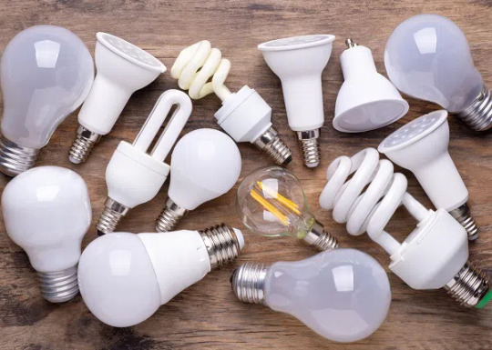
Understanding Heat Resistant LED Lights
Heat resistant LED lights are engineered with advanced materials and thermal management systems that allow them to operate efficiently at elevated temperatures, sometimes exceeding 150°C. Unlike standard LEDs, which may degrade or fail under heat stress, these robust LEDs incorporate heat sinks, specialized coatings, and resilient semiconductor materials. This ensures consistent brightness, reduced energy consumption, and a longer operational life span in harsh conditions.
Key Drivers Propelling Market Growth
One of the primary drivers behind the growth of the heat resistant LED lights market is the expanding industrial sector. Manufacturing plants, metal processing units, and chemical factories often have environments where ambient temperatures soar. Traditional lighting in such conditions not only risks premature burnout but also poses safety hazards. Heat resistant LEDs offer a safer, energy-efficient alternative, reducing maintenance costs and downtime.
Additionally, the automotive industry is witnessing a rising demand for heat resistant LEDs, particularly in engine compartments, brake lights, and headlamps. Vehicles, especially electric and high-performance models, generate significant heat, and these LEDs help enhance reliability and safety.
The aerospace and defense sectors also contribute to market expansion. Aircraft cabins, cockpits, and exterior lighting systems require durable LEDs capable of operating under extreme thermal fluctuations and vibrations. Heat resistant LEDs ensure optimal performance and energy efficiency in these critical applications.
Innovations Driving Technological Advancements
Technological innovations are a cornerstone of the heat resistant LED lights market. Manufacturers are focusing on developing LEDs with enhanced thermal conductivity through the use of novel substrates such as ceramics and metal-core printed circuit boards (MCPCBs). These materials dissipate heat more effectively than traditional plastic or fiberglass boards.
Another breakthrough is in encapsulation technology. Heat resistant LEDs use specially formulated silicone and epoxy resins that protect the internal components from thermal degradation while maintaining transparency for optimal light output.
Smart lighting solutions are being integrated with heat resistant LEDs as well. Sensors and controllers can monitor temperature and adjust brightness levels dynamically to prevent overheating, further extending the LED lifespan and energy savings.
Market Segmentation and Applications
The heat resistant LED lights market is segmented based on product type, application, and end-user industry. Key product categories include high-power LEDs, LED modules, and LED strips, each designed to meet specific heat resistance requirements.
In terms of applications, industrial lighting leads the demand due to the necessity for durable and energy-efficient lighting in factories, warehouses, and processing plants. Automotive lighting is another major segment, as heat resistant LEDs improve vehicle safety and aesthetics.
Other notable applications include outdoor lighting for high-temperature climates, marine lighting, and specialty lighting for equipment such as ovens, furnaces, and heat exchangers. These diverse applications underscore the versatility and critical importance of heat resistant LED technology.
Regional Insights
Asia-Pacific holds a significant share of the heat resistant LED lights market, driven by rapid industrialization and automotive manufacturing in countries like China, India, and Japan. Investments in smart factories and green energy initiatives further boost adoption in this region.
North America and Europe also exhibit robust market growth due to stringent energy efficiency regulations and growing awareness of LED benefits. These regions focus heavily on research and development, fostering innovation in heat resistant LED materials and designs.
Challenges and Market Restraints
Despite the promising outlook, the heat resistant LED lights market faces several challenges. The higher initial cost of these specialized LEDs compared to conventional lighting can be a barrier for small and medium enterprises. Additionally, the complexity involved in designing heat resistant LEDs that maintain optimal light quality at high temperatures requires advanced manufacturing capabilities.
Another restraint is the competition from alternative lighting technologies such as high-intensity discharge (HID) lamps and halogen lights, which still find usage in certain extreme environments despite their inefficiencies.
Future Outlook and Opportunities
The future of the heat resistant LED lights market is bright, with significant growth opportunities on the horizon. Increasing emphasis on energy conservation and sustainable industrial practices will continue to drive demand. Moreover, ongoing research into novel materials such as gallium nitride (GaN) and advances in nano-coatings are expected to enhance heat resistance and LED efficiency further.
Emerging applications in electric vehicles, renewable energy installations, and smart cities offer new avenues for market expansion. The integration of heat resistant LEDs with Internet of Things (IoT) platforms can enable predictive maintenance and adaptive lighting systems, making these lights more intelligent and user-friendly.
Conclusion
The Heat Resistant LED Lights Market features a dynamic and rapidly evolving sector that addresses the critical need for durable, energy-efficient lighting solutions in high-temperature environments. By combining cutting-edge materials science with innovative design, these LEDs are redefining how industries illuminate their operations under extreme conditions. As technology advances and awareness grows, heat resistant LED lights are poised to become indispensable in sectors demanding reliability, safety, and sustainability in lighting.
0 notes
Text
LED is the abbreviation of light emitting diode (Light Emitting Diode, LED),
LED is the abbreviation of light emitting diode (Light Emitting Diode, LED), also known as light emitting diode, this semiconductor element is generally used as an indicator light, a display panel, it can not only efficiently directly convert electrical energy into light energy, but also has up to tens of thousands of hours~ 100,000 hours of service life, while not as fragile as traditional bulbs, and can save electricity and other advantages.
However, no matter what kind of LED, it needs to be reasonably designed for different types of packaging, because only the packaged ones can become end point products and be put into practical application.
1. Why should LEDs be encapsulated?
The function of LED packaging is to connect the outer leads to the electrodes of the LED chip, which not only protects the LED chip, but also improves the luminous efficiency. Therefore, LED packaging not only completes the output of electrical signals, but also protects the normal operation of the die and outputs visible light. It can be seen that LED packaging has both electrical parameters and optical parameters design and technical requirements, which is not a simple task.
2. LED packaging equipment
Due to the high requirements of LED packaging, whether it is an in-line LED or a patch LED, a high-precision solid crystal machine must be used, because whether the position of the LED chip into the package is accurate will directly affect the luminous efficiency of the whole package device. If the position of the chip in the reflective cup is deviated, the light cannot be completely reflected, which directly affects the brightness of the LED. However, with an advanced PR System (pre-image recognition system) solid crystal machine, the LED chip can still be precisely soldered to the predetermined position regardless of the quality of the lead frame.
3. LED package form
According to different applications, different external dimensions, heat dissipation schemes and luminous effects. LED packaging forms are various. At present, LEDs are mainly classified according to packaging forms: Lamp-LED, TOP-LED, Side-LED, SMD-LED, High-Power-LED, Flip Chip-LED, etc
Lamp-LED (Vertical LED)
The early appearance of Lamp-LED is in-line LED, which is packaged in the form of potting. The process of potting is to inject liquid epoxy resin into the LED molding cavity, then insert a pressure-welded LED bracket, put it in an oven to let the epoxy resin cure, and then detach the LED from the cavity and form it immediately. Due to the relatively simple manufacturing process and low cost, it has a high market share.
SMD-LED (surface adhesive LED)
SMD LED is attached to the surface of the circuit board, suitable for SMT processing, reflow soldering, which solves the problems of brightness, viewing angle, flatness, reliability, consistency, etc., using lighter PCB board and reflective layer materials. After improvement, the heavier carbon steel material pins of the in-line LED are removed, so that the display reflective layer needs to be filled with less epoxy resin, the purpose is to reduce the size and weight. In this way, the surface mount LED can easily reduce the weight of the product by half, ultimately making the application more perfect.
Side-LED (side-emitting LED)
At present, another key point of LED packaging is the side-emitting package. If you want to use LED as the backlight source of LCD (liquid crystal display), the side-emitting light of LED needs to be the same as the surface-emitting light, so that the LCD backlight emits evenly. Although the design of the lead frame can also achieve the purpose of side-emitting light, the heat dissipation effect is not good. However, Lumileds invented the design of the mirror, which uses the principle of the mirror to emit side light, and successfully applies high-power LEDs to large-size LCD backlight modules.
TOP-LED (top-emitting LED)
The top light-emitting LED is a relatively common SMD light-emitting diode. Mainly used in backlights and status indicators in multi-function ultra-thin mobile phones and PDAs.
High-Power-LED (High Power LED)
In order to obtain high-power and high-brightness LED light sources, manufacturers have developed high-power LED chip and package designs. At present, LED packages that can withstand several W of power have appeared. For example, the package structure of Norlux series high-power LEDs is a multi-chip combination with a hexagonal aluminum plate as a base (making it non-conductive). The base diameter is 31.75mm, and the light-emitting region is located in its center. The diameter is about (0.375 × 25.4) mm, which can accommodate 40 LED dies. The aluminum plate is used as a heat sink at the same time. This package adopts a conventional die high-density combination package, which has high luminous efficiency, low thermal resistance, and high light output power under high current. It is also a promising LED solid light source.
It can be seen that the thermal characteristics of power LED directly affect the operating temperature, luminous efficiency, luminous wavelength, and service life of LED, etc. Therefore, the packaging design and manufacturing technology of power LED chips are even more important.
Flip Chip-LED (Clad Crystal LED)
The LED overlay packaging structure is basically made with a plurality of perforations in the PCB, and each perforation on one side of the substrate is provided with two different areas of conductive material that are open to each other, and the conductive material is tiled on the substrate. On the surface, there are a plurality of unpackaged LED chips placed at each perforation on the side of the conductive material. The positive and negative contacts of a single LED chip are connected with the conductive material on the substrate surface by solder balls, respectively, and on the surface of the side of the plurality of LED chips facing the perforation, there is a transparent sealant. The sealant is in the shape of a half sphere and is located at each perforation. It belongs to flip-chip light emitting diodes.
conclusion
According to the principle of solid-state light-emitting physics, the luminous efficiency of LED is approximately 100%. Therefore, LED is known as a new light source in the 21st century, and is expected to become the fourth generation light source after incandescent lamps, fluorescent lamps, and high-intensity gas discharge lamps. Looking to the future, manufacturers will definitely place high-power and high-brightness LEDs in a prominent development position. The substrate, epitaxy, chip, packaging, and application in the LED industry chain need to be jointly developed and cultivated by multiple parties. Packaging is the upper and lower parts of the industry chain, and requires great attention and attention from everyone.
0 notes
Text
Hydrogenated Bisphenol A (HBPA) Epoxy Resin Market, Global Outlook and Forecast 2025-2032
Hydrogenated Bisphenol A Epoxy Resin Market Size, Demand & Supply, Regional and Competitive Analysis 2025-2031
Market Size
The global Hydrogenated Bisphenol A Epoxy Resin market was valued at USD 30 million in 2023 and is expected to reach USD 40.89 million by 2032, growing at a CAGR of 3.50% during the forecast period.
Key Market Statistics:
Download a free Sample Report PDF
Market Size in 2023: USD 30 million
Projected Market Size by 2032: USD 40.89 million
CAGR (2023-2032): 3.50%
This steady growth is driven by increased demand in the coatings, automotive, electronics, and construction industries, which are looking for high-performance materials with excellent durability and resistance to environmental elements. As the global manufacturing sector grows and modernizes, the need for more advanced materials like HBPA Epoxy Resin is expanding.
Hydrogenated Bisphenol A Epoxy Resin (HBPA) is a specialized type of epoxy resin derived from hydrogenated bisphenol A. Known for its excellent weather resistance and low viscosity, HBPA is widely utilized in a variety of industries. However, unlike conventional bisphenol A-based epoxy resins, HBPA requires a longer gelation time and possesses unique attributes that enhance its performance in certain applications. This article will provide a comprehensive, SEO-friendly analysis of the global HBPA Epoxy Resin market, including its definition, market size, dynamics, regional analysis, and much more.
Definition
Hydrogenated Bisphenol A Epoxy Resin (HBPA) is a type of epoxy resin produced by hydrogenating bisphenol A (BPA). The hydrogenation process involves adding hydrogen molecules to the BPA compound to alter its structure, resulting in an epoxy resin with superior stability, durability, and resistance to weathering.
Key Characteristics of HBPA Epoxy Resin:
Low Viscosity: The resin has a very low viscosity, making it comparable to DGEBF (diglycidyl ether of bisphenol F), allowing for easier processing and application.
Longer Gelation Time: Unlike conventional DGEBA (diglycidyl ether of bisphenol A) resins, HBPA has a much longer gelation time, often requiring more than twice the amount of time to fully gel.
Excellent Weather Resistance: One of the standout features of HBPA is its exceptional resistance to environmental factors, including UV exposure and humidity. This makes it ideal for outdoor applications and products that are exposed to harsh weather conditions.
Primary Applications of HBPA Epoxy Resin:
Coatings and Paints: Used in protective coatings for structures and vehicles, HBPA provides excellent outdoor durability and weather resistance.
Electronics: In the electronics industry, HBPA is utilized for encapsulation and coatings that require good electrical properties and long-term stability.
Automotive: In the automotive sector, HBPA is used for coatings and adhesives due to its strong adhesion and resistance to chemicals and environmental stress.
Construction: HBPA resins are used in adhesives and sealants, where long-lasting performance and weatherability are essential.
Due to its enhanced durability and superior properties compared to conventional resins, HBPA Epoxy Resin is increasingly becoming a material of choice for high-performance applications.
Global Hydrogenated Bisphenol A (HBPA) Epoxy Resin: Market Segmentation Analysis
This report provides a deep insight into the global Hydrogenated Bisphenol A Epoxy Resin market, covering all its essential aspects. This ranges from a macro overview of the market to micro details of the market size, competitive landscape, development trends, niche market, key market drivers and challenges, SWOT analysis, value chain analysis, etc.
The analysis helps the reader shape the competition within the industries and strategies for the competitive environment to enhance potential profit. Furthermore, it provides a simple framework for evaluating and assessing the position of the business organization. The report structure also focuses on the competitive landscape of the HBPA Epoxy Resin market, introducing the market share, performance, product situation, and operation situation of the main players, helping readers understand the competition pattern.
In a word, this report is a must-read for industry players, investors, researchers, consultants, business strategists, and all those who have a stake or are planning to foray into the HBPA Epoxy Resin market in any manner.
Market Segmentation (by Application)
Automotive
Electronics
Construction
Industrial Coatings
Others
Market Segmentation (by Type)
Liquid HBPA Epoxy Resin
Solid HBPA Epoxy Resin
Key Company
Hexion Inc.
Huntsman International LLC
Kraton Polymers
Olin Corporation
Get The Complete Report &TOC
FAQs
1.What is the current market size of the Hydrogenated Bisphenol A Epoxy Resin market?
The Hydrogenated Bisphenol A Epoxy Resin market was valued at USD 30 million in 2023 and is projected to reach USD 40.89 million by 2032.
2.Which are the key companies operating in the Hydrogenated Bisphenol A Epoxy Resin market?
Key companies include Hexion Inc., Huntsman International LLC, Kraton Polymers, and Olin Corporation.
3.What are the key growth drivers in the Hydrogenated Bisphenol A Epoxy Resin market?
Key growth drivers include increasing demand in automotive, construction, and electronics industries, along with the rise in demand for durable and weather-resistant materials.
4.Which regions dominate the Hydrogenated Bisphenol A Epoxy Resin market?
North America, Europe, and Asia-Pacific dominate the market, with significant growth in the Asia-Pacific region.
5.What are the emerging trends in the Hydrogenated Bisphenol A Epoxy Resin market?
Emerging trends include the growing adoption of HBPA Epoxy Resin in green construction, electric vehicles, and electronics manufacturing, driven by their superior durability and resistance properties
0 notes
Text
How to Use Epoxy Adhesives for Preventive Maintenance in Industries?
Due to heavy loads, harsh environmental conditions and continuous operation, industrial equipment and structures are subjected to constant wear and tear. Industries rely on epoxy adhesives for preventive maintenance to avoid costly repairs and downtime. These high-performance bonding solutions offer exceptional strength, durability and resistance to chemicals, heat and moisture. This makes them ideal for industrial applications.
If you are looking to enhance the longevity of machinery and infrastructure, here’s how epoxy adhesives can be used for preventive maintenance.
1. Strengthening and Repairing Metal Components
Metal surfaces in industries often suffer from corrosion, cracks and surface wear. Epoxy adhesives provide a strong bond that reinforces weak areas, preventing further deterioration. Whether it is sealing a crack in a machine casing or repairing a worn-out shaft, epoxy resin ensures long-lasting adhesion, reducing the risk of sudden breakdowns.
2. Securing Loose Fasteners and Joints
Bolts, screws and fasteners can loosen over time due to constant vibration and movement in machinery. Applying epoxy resin to these connections creates a firm grip. This prevents loosening and maintaining structural integrity. This is particularly beneficial in industries such as automotive, aerospace and heavy machinery, where secure joints are critical for safety and efficiency.
3. Preventing Leaks in Pipes and Tanks
Leaks in pipelines and storage tanks can lead to serious operational hazards and material losses. Using epoxy adhesives, industries can seal minor cracks and leaks before they escalate into major failures. With excellent chemical and moisture resistance, epoxy resin ensures a tight seal that withstands high pressure and harsh substances.
4. Reinforcing Concrete Floors and Structures
Industrial floors and structures endure heavy loads and foot traffic, which leads to cracks and surface damage. Epoxy adhesives can be used to fill gaps and reinforce concrete surfaces, preventing further degradation. Additionally, epoxy resin coatings enhance floor durability, which makes them resistant to impact, abrasion and chemicals.
5. Insulating and Protecting Electrical Components
In electrical and electronic industries, epoxy resin is widely used for insulation and encapsulation of sensitive components. It protects circuits, connectors and transformers from moisture, dust and chemical exposure. This ensures uninterrupted performance and reduces the risk of short circuits.
Implementing epoxy adhesives in preventive maintenance helps industries reduce downtime, increase equipment lifespan and improve overall efficiency. Their versatility and strength make them essential for repairing, reinforcing and protecting industrial assets. Regular use of epoxy resin in maintenance strategies ensures long-term reliability, minimising unexpected failures and costly repairs. Investing in high-quality epoxy adhesives is a smart choice for industries looking to enhance operational resilience.
0 notes
Text
Long-Term Reliability Studies of Epoxy Encapsulation in Electronics

Epoxy encapsulation plays a critical role in ensuring the durability and operational stability of electronic components over extended periods. Used widely in sectors like consumer electronics, automotive systems, and industrial automation, epoxy encapsulation protects sensitive electronic parts from moisture, dust, vibration, thermal fluctuations, and corrosive chemicals. As devices become smaller and more complex, the demand for long-term reliability in encapsulated electronics has significantly increased.
The formulation of the epoxy resin used is a critical determinant of long-term reliability. Factors such as cure chemistry, filler content, and thermal conductivity directly influence how well the encapsulant protects electronic components. High-performance epoxy systems are designed to maintain mechanical integrity and electrical insulation properties even under severe environmental stress. Innovations in resin technology now include thermally conductive epoxies, UV-resistant formulations, and low-viscosity systems for precision encapsulation.
Long-term reliability studies typically evaluate the performance of epoxy encapsulation under accelerated aging conditions. These studies simulate years of exposure to extreme temperatures, humidity cycles, and mechanical stress to predict potential failure modes. Common test methods include thermal shock testing, high-humidity aging, dielectric breakdown tests, and adhesion strength analysis. The results help manufacturers refine encapsulation processes, resin compositions, and design strategies to enhance product longevity.
In India, several epoxy resin manufacturers support the growing electronics industry by offering custom formulations tailored for long-term performance. These companies play a vital role in supplying encapsulants that meet international quality standards for durability and safety. The right choice of epoxy resin ensures not just initial performance but sustained reliability over the device’s operational life.
For electronics manufacturers seeking proven reliability and material consistency, partnering with experienced suppliers is essential. MB Enterprises, a trusted name among epoxy resin manufacturers in India, offers specialized epoxy encapsulation solutions developed for long-term durability in electronic applications.

0 notes
Text
Plastic Encapsulated Thermistor Market: Transition to Advanced Nodes in Semiconductor Fabrication
MARKET INSIGHTS
The global Plastic Encapsulated Thermistor size was valued at US$ 234 million in 2024 and is projected to reach US$ 323 million by 2032, at a CAGR of 4.6% during the forecast period 2025-2032. The U.S. market accounted for 28% of global revenue in 2024, while China’s market is expected to grow at a faster CAGR of 6.7% through 2032.
Plastic Encapsulated Thermistors are temperature-sensitive resistors encapsulated in polymer materials, offering improved mechanical protection and environmental resistance compared to bare thermistors. These components exhibit a predictable change in electrical resistance with temperature variations, making them critical for temperature sensing and compensation applications across industries. The product range includes both uninsulated wire and insulated wire variants, with the latter dominating over 62% market share in 2024 due to better safety and durability.
Market growth is driven by expanding applications in home appliances, digital thermometers, and medical devices, where precise temperature monitoring is essential. While demand from automotive applications shows steady growth, the medical sector is emerging as the fastest-growing segment with a projected 7.1% CAGR, fueled by increasing adoption in diagnostic equipment and patient monitoring systems. Key manufacturers like Littlefuse and Semitec are investing in miniaturization technologies to capture opportunities in wearable medical devices and IoT applications.
MARKET DYNAMICS
MARKET DRIVERS
Expanding Automotive and Electronics Sectors Fuel Demand for Plastic Encapsulated Thermistors
The global automotive industry’s shift toward electric vehicles and advanced driver-assistance systems (ADAS) is creating substantial demand for reliable temperature sensors like plastic encapsulated thermistors. Modern vehicles contain over 50 temperature sensors on average, with thermistors playing a crucial role in battery management, climate control, and engine monitoring systems. The growing complexity of automotive electronics, combined with stringent safety regulations, is pushing manufacturers toward encapsulated solutions that offer better protection against environmental factors.
Growth in Smart Home Appliances Accelerates Market Penetration
The smart home appliance market, projected to maintain double-digit growth through 2030, represents a significant growth avenue for plastic encapsulated thermistors. These components are essential for temperature regulation in refrigerators, air conditioners, and washing machines. The encapsulation provides necessary protection against moisture and chemical exposure while maintaining precise temperature sensitivity. With consumers increasingly opting for energy-efficient appliances featuring IoT connectivity, manufacturers are incorporating more sophisticated thermal management systems that rely heavily on encapsulated thermistor technology.
➤ The Asia Pacific region accounts for over 40% of global appliance production, making it a critical market for thermistor suppliers looking to capitalize on this growth.
Furthermore, the medical equipment sector’s expansion, particularly in portable diagnostic devices and wearable health monitors, presents additional growth opportunities. These applications require miniaturized, reliable temperature sensors that can withstand sterilization processes and body fluid exposure.
MARKET RESTRAINTS
Raw Material Price Volatility Impacts Profit Margins
The plastic encapsulated thermistor market faces significant pressure from fluctuating raw material costs. The prices of key materials like epoxy resins, nickel, and specialty plastics have shown volatility exceeding 15% year-over-year in recent periods. This unpredictability makes cost management challenging for manufacturers, particularly smaller players with limited procurement leverage. The situation is further complicated by global supply chain disruptions that have affected material availability since 2020.
Other Constraints
Intense Commoditization Pressure The market has seen increasing price competition as numerous Asian manufacturers enter the space with lower-cost alternatives. While encapsulation provides differentiation, many basic thermistor applications face severe commoditization, squeezing margins for all participants.
Technical Limitations in Extreme Environments Despite their advantages, plastic encapsulated thermistors face operational challenges in applications requiring continuous exposure to temperatures above 150°C or aggressive chemical environments. This limitation restricts their use in certain industrial and automotive applications where ceramic or glass-encapsulated alternatives remain preferred.
MARKET CHALLENGES
Miniaturization Demands Strain Manufacturing Capabilities
The industry faces mounting pressure to produce smaller thermistors with equivalent or improved performance characteristics. Modern electronics, particularly wearables and IoT devices, require components measuring less than 1mm in diameter while maintaining tight resistance tolerances. Achieving this miniaturization without compromising reliability or increasing failure rates presents significant engineering and production challenges. The encapsulation process becomes particularly difficult at these scales, with yield rates suffering when dimensions shrink below certain thresholds.
Other Challenges
Stringent Automotive Qualification Processes The automotive industry’s stringent qualification requirements, including AEC-Q200 compliance, create lengthy and expensive certification processes. Many manufacturers struggle with the extensive testing and documentation requirements, delaying time-to-market for new products.
Maintaining Consistency Across Production Batches Achieving consistent performance characteristics across large production runs remains an ongoing challenge due to variations in plastic curing processes and raw material properties. This consistency is critical for applications requiring precise temperature measurement and control.
MARKET OPPORTUNITIES
Emerging Applications in Renewable Energy Systems Create New Growth Avenues
The rapid expansion of solar and wind energy infrastructure presents significant opportunities for plastic encapsulated thermistors. These components are increasingly used in battery storage systems, power inverters, and turbine monitoring equipment. The renewable energy sector’s projected 8% annual growth through 2032 suggests strong continued demand for reliable temperature monitoring solutions that can withstand outdoor environmental conditions.
Advancements in Encapsulation Materials Open New Possibilities
Recent developments in polymer science have yielded encapsulation materials with enhanced thermal conductivity and chemical resistance. These innovations enable thermistors to operate in previously inaccessible applications, including certain industrial processes and medical sterilization equipment. As material science continues progressing, we can expect expanded application boundaries for plastic encapsulated solutions.
Additionally, the integration of smart manufacturing techniques like AI-powered quality control and Industry 4.0 practices is helping manufacturers overcome previous production challenges. These technologies enable real-time process adjustments and predictive maintenance, significantly improving yield rates and product consistency.
PLASTIC ENCAPSULATED THERMISTOR MARKET TRENDS
Growing Demand Across Consumer Electronics and Automotive Sectors
The global Plastic Encapsulated Thermistor market continues to gain traction, primarily driven by increasing adoption in consumer electronics and automotive applications. Thermistors play a critical role in temperature sensing and circuit protection, making them indispensable in smart home devices, HVAC systems, and automotive battery management. The rise of IoT-enabled appliances and electric vehicles (EVs) has further accelerated demand, with market forecasts projecting a steady CAGR throughout the decade. Advances in polymer encapsulation technology have enhanced their durability and resistance to environmental factors, further expanding their utility in high-performance applications.
Other Trends
Miniaturization and Precision Engineering
Manufacturers are focusing on miniaturization to meet the evolving needs of compact electronic devices. Smaller form factors with enhanced thermal sensitivity are increasingly sought after in wearable technology and medical devices. Improved fabrication techniques allow for thermistors that maintain accuracy while reducing footprint—critical for applications like implantable medical sensors and precision instrumentation. Additionally, innovations in material science have led to better stability over wide temperature ranges, addressing key challenges in industrial automation.
Regional Market Dynamics and Supply Chain Optimization
While North America and Europe remain dominant markets due to stringent automotive safety regulations and advanced healthcare infrastructure, Asia-Pacific is emerging as the fastest-growing region. Countries like China and India are witnessing double-digit growth in thermistor shipments, fueled by expanding electronics manufacturing hubs and government incentives for EV adoption. Meanwhile, suppliers are increasingly focusing on vertical integration to mitigate raw material shortages, with leading companies investing in proprietary polymer compounds to ensure consistency and reduce lead times. Partnerships between sensor manufacturers and semiconductor foundries are also streamlining production workflows, directly benefiting OEMs.
Sustainability and Regulatory Compliance
Environmental regulations are reshaping material selection, with RoHS-compliant thermistors now constituting over 70% of new product launches. The shift toward halogen-free encapsulation materials aligns with global sustainability initiatives while maintaining performance benchmarks. Recycling programs for end-of-life electronic components are gaining momentum, particularly in Europe, where circular economy policies incentivize eco-friendly designs. These trends are expected to influence R&D priorities, particularly in balancing cost efficiency with compliance—a crucial factor for price-sensitive markets.
COMPETITIVE LANDSCAPE
Key Industry Players
Innovation and Strategic Positioning Drive Market Competition
The global plastic encapsulated thermistor market features a dynamic competitive landscape with a mix of established players and emerging manufacturers striving for market share. With Asia-Pacific dominating production capacity, regional players continue gaining ground on traditional Western manufacturers through cost-effective solutions.
Market leader Littelfuse maintains approximately 18% revenue share in 2024, leveraging its extensive distribution channels globally and premium product positioning in medical and industrial applications. The company recently expanded its NTC thermistor portfolio with high-precision variants certified for automotive applications, strengthening its market position.
Meanwhile, Semitec has emerged as the fastest-growing competitor, achieving 12% year-over-year growth in 2024 through targeted expansions in smart home appliance markets. Their patented encapsulation technology provides superior moisture resistance compared to industry standards, making them preferred suppliers for humid environment applications.
Chinese manufacturers including Shenzhen Minchuang Electronics and NDF collectively account for over 30% of global thermistor unit production, primarily serving domestic appliance manufacturers and export markets. Their competitive pricing continues to disrupt traditional pricing models, forcing multinational players to optimize manufacturing costs.
The market also sees increasing specialization, with companies like Kemit Sensing Technology focusing exclusively on medical-grade thermistors featuring biocompatible encapsulants. This trend toward application-specific solutions is reshaping competitive dynamics across price-performance segments.
List of Key Plastic Encapsulated Thermistor Manufacturers:
Littelfuse (U.S.)
Semitec (Japan)
NDF (Germany)
MINJIE TECHNOLOGY (China)
Kemit Sensing Technology (China)
Shenzhen Minchuang Electronics Co., Ltd. (China)
Fuwen (China)
Shenzhen Nuoruisi TechnologyCo., Ltd (China)
Dongguan Tianrui Electronics Co., Ltd (China)
Segment Analysis:
By Type
Uninsulated Wire Segment Holds Significant Share Due to Cost-Effectiveness and Widespread Use in Consumer Electronics
The market is segmented based on type into:
Uninsulated Wire
Subtypes: Bead type, Disc type, and others
Insulated Wire
Subtypes: Epoxy-coated, Silicone-coated, and others
By Application
Home Appliance Segment Dominates Due to Increasing Demand for Temperature Sensors in Smart Devices
The market is segmented based on application into:
Home Appliance
Digital Thermometer
Medical
Automotive
Others
By End User
Consumer Electronics Sector Leads Owing to Rising Adoption of Temperature Sensing Components
The market is segmented based on end user into:
Consumer Electronics
Healthcare
Automotive
Industrial
Regional Analysis: Plastic Encapsulated Thermistor Market
North America The North American market for Plastic Encapsulated Thermistors is driven by advanced manufacturing capabilities and stringent quality standards, particularly in the medical and automotive sectors. With the U.S. accounting for the majority of regional demand, manufacturers are focusing on high-precision components for applications like patient monitoring devices and electric vehicle battery management systems. The presence of key players like Littelfuse and Semitec further strengthens the supply chain. However, rising material costs and competition from Asian suppliers remain challenges. Environmental regulations promoting lead-free electronics are accelerating innovation in thermistor materials and encapsulation techniques.
Europe Europe’s market emphasizes energy efficiency and miniaturization, with Germany leading in industrial automation applications. The region’s medical device regulations (MDR) and automotive safety standards create demand for reliable, long-life thermistors. EU directives on hazardous substances (RoHS/REACH) are pushing manufacturers toward halogen-free plastic encapsulation. While Western Europe shows steady growth, Eastern Europe presents opportunities for cost-competitive production. The market is somewhat constrained by the shift toward integrated temperature sensing solutions in consumer electronics, though niche applications in HVAC and renewable energy systems offer stability.
Asia-Pacific As the largest and fastest-growing market, Asia-Pacific benefits from China’s dominance in electronics manufacturing and India’s expanding HVAC sector. Chinese firms like Shenzhen Minchuang Electronics hold significant market share by offering competitively priced products. Japan and South Korea drive demand for high-accuracy thermistors in automotive and robotics. The region faces price sensitivity, prompting suppliers to balance cost-cutting with quality—leading to a bifurcation between budget and premium offerings. Local governments’ investments in 5G infrastructure and IoT devices are creating new application avenues, particularly for insulated wire-type thermistors.
South America Market growth in South America is uneven, with Brazil’s automotive aftermarket and Argentina’s agricultural equipment sector being primary demand drivers. Infrastructure limitations hinder large-scale electronics production, making the region reliant on imports—chiefly from China. Economic volatility affects procurement cycles, though the medical device industry shows resilience due to public health investments. Manufacturers face challenges in building local distribution networks but can leverage Brazil’s growing appliance manufacturing base. The lack of standardized testing facilities impacts quality perception among buyers.
Middle East & Africa This emerging market is propelled by construction-related HVAC projects in the GCC countries and increasing electronics assembly in Turkey. While currently a small percentage of global demand, the region shows potential in oil & gas temperature monitoring and renewable energy systems. South Africa serves as a gateway for thermistor distribution to neighboring countries. The market is price-driven with limited local production, though UAE-based distributors are expanding value-added services. Political instability in parts of North Africa and inconsistent regulatory frameworks slow adoption rates compared to other regions.
Report Scope
This market research report provides a comprehensive analysis of the global and regional Plastic Encapsulated Thermistor markets, covering the forecast period 2024–2032. It offers detailed insights into market dynamics, technological advancements, competitive landscape, and key trends shaping the industry.
Key focus areas of the report include:
Market Size & Forecast: Historical data and future projections for revenue, unit shipments, and market value across major regions and segments. The global market was valued at USD XX million in 2024 and is projected to reach USD XX million by 2032.
Segmentation Analysis: Detailed breakdown by product type (Uninsulated Wire, Insulated Wire), application (Home Appliance, Digital Thermometer, Medical, Others), and end-user industry to identify high-growth segments.
Regional Outlook: Insights into market performance across North America, Europe, Asia-Pacific, Latin America, and Middle East & Africa, including country-level analysis. The U.S. market size is estimated at USD XX million in 2024 while China is projected to reach USD XX million.
Competitive Landscape: Profiles of leading market participants including NDF, MINJIE TECHNOLOGY, Kemit Sensing Technology, Littlefuse, Semitec, and others, covering their product portfolios, market share (top five players held approximately XX% in 2024), and strategic developments.
Technology Trends & Innovation: Assessment of emerging encapsulation technologies, material advancements, and integration trends in electronics applications.
Market Drivers & Restraints: Evaluation of factors including growing demand for temperature sensors in consumer electronics, medical devices, and industrial applications, along with supply chain challenges and raw material price fluctuations.
Stakeholder Analysis: Strategic insights for component manufacturers, OEMs, distributors, and investors regarding market opportunities and challenges.
Related Reports:https://semiconductorblogs21.blogspot.com/2025/06/chip-solid-tantalum-capacitor-market.htmlhttps://semiconductorblogs21.blogspot.com/2025/06/global-electrical-resistance-probes.htmlhttps://semiconductorblogs21.blogspot.com/2025/06/high-temperature-tantalum-capacitor.htmlhttps://semiconductorblogs21.blogspot.com/2025/06/global-link-choke-market-innovations.htmlhttps://semiconductorblogs21.blogspot.com/2025/06/multirotor-brushless-motors-market.htmlhttps://semiconductorblogs21.blogspot.com/2025/06/planar-sputtering-target-market.htmlhttps://semiconductorblogs21.blogspot.com/2025/06/ferrite-core-choke-market-opportunities.htmlhttps://semiconductorblogs21.blogspot.com/2025/06/float-zone-silicon-crystal-market.htmlhttps://semiconductorblogs21.blogspot.com/2025/06/carbon-composition-resistors-market.htmlhttps://semiconductorblogs21.blogspot.com/2025/06/resistor-network-array-market-analysis.htmlhttps://semiconductorblogs21.blogspot.com/2025/06/melf-resistors-market-key-drivers-and.htmlhttps://semiconductorblogs21.blogspot.com/2025/06/metal-foil-resistors-market.htmlhttps://semiconductorblogs21.blogspot.com/2025/06/metal-oxidation-resistors-market-size.htmlhttps://semiconductorblogs21.blogspot.com/2025/06/ferrite-toroid-coils-market-growth.htmlhttps://semiconductorblogs21.blogspot.com/2025/06/vacuum-fluorescent-displays-market.html
0 notes
Text
X-Ray Inspection in Electronics Manufacturing: Detecting Hidden Defects in PCBs and Semiconductors

Electronics manufacturing has evolved significantly, with devices becoming smaller, more complex, and highly integrated. The demand for high-quality printed circuit boards (PCBs) and semiconductors has increased, making defect detection more critical than ever. Traditional visual inspections and electrical tests often fail to detect hidden defects that lie beneath the surface of electronic components. This is where X-ray inspection plays a vital role in ensuring the reliability, functionality, and longevity of electronic products.
In this article, we will explore how X-ray inspection is transforming electronics manufacturing by detecting defects that are otherwise invisible, ensuring quality control, and reducing failure rates in electronic components.
1. Why X-Ray Inspection is Essential in Electronics Manufacturing
X-ray inspection, also known as X-ray non-destructive testing (NDT), is a powerful technique used to examine the internal structure of PCBs and semiconductors without causing damage. Unlike optical inspection methods, X-ray imaging allows manufacturers to:
Detect hidden defects inside components.
Inspect solder joints, connections, and traces beneath layers of circuitry.
Identify cracks, voids, and misalignments in semiconductor chips.
Improve quality control and reduce the risk of field failures.
With increasing complexity in miniaturized electronics, traditional inspection techniques like Automated Optical Inspection (AOI) and in-circuit testing (ICT) are often insufficient, making X-ray inspection a necessity for modern electronics production.
2. Common Defects Detected by X-Ray Inspection
X-ray imaging is used to identify defects in various stages of PCB assembly and semiconductor fabrication. Here are some of the most common issues detected:
A. Solder Joint Defects
With the widespread use of Surface Mount Technology (SMT), solder joints have become smaller and more compact, making them harder to inspect visually. X-ray inspection helps detect:
Cold Solder Joints – Incomplete melting of solder, leading to weak electrical connections.
Solder Bridges – Unwanted solder connections between adjacent pads, causing short circuits.
Head-in-Pillow (HIP) Defects – Poor solder bonding due to contamination or misalignment.
Voids in Solder Joints – Air pockets within solder that weaken structural integrity and cause performance issues.
B. Component Alignment Issues
With increasing use of Ball Grid Array (BGA), Quad Flat No-lead (QFN), and Chip-Scale Package (CSP) components, misalignment and soldering defects are major concerns. X-ray inspection can reveal:
Misaligned BGAs – Improperly placed BGA components can lead to failed connections.
Open Circuits – Breaks in solder joints that prevent electrical continuity.
Tombstoning – When a small passive component (like a capacitor) tilts or stands upright due to uneven heating.
C. Voids and Cracks in Semiconductor Packaging
Semiconductor chips and microprocessors are prone to micro-cracks, delaminations, and voids due to thermal stress and manufacturing defects. X-ray imaging can detect:
Cracks in Silicon Die – Tiny fractures that can cause failure under thermal cycling.
Delamination of Layers – Separation between layers in a multi-layer semiconductor package.
Air Voids in Encapsulation – Gaps in epoxy or underfill material that can compromise chip performance.
D. Wire Bonding and Interconnect Defects
For integrated circuits (ICs) and microchips, X-ray imaging helps check:
Broken or Weak Wire Bonds – Ensuring strong electrical connections inside the IC.
Short Circuits in Multi-layer PCBs – Detecting unwanted conductive paths inside the PCB stack-up.
3. Types of X-Ray Inspection Systems Used in Electronics Manufacturing
Manufacturers use different types of X-ray inspection systems depending on the complexity of the components being tested.
A. 2D X-Ray Inspection
Provides a flat, two-dimensional image of the PCB or semiconductor.
Useful for identifying simple soldering defects and misalignments.
B. 3D X-Ray Computed Tomography (CT)
Offers a layer-by-layer 3D view of internal structures.
Ideal for inspecting multi-layer PCBs and advanced semiconductor packaging.
C. Automated X-Ray Inspection (AXI)
A high-speed automated solution for mass production environments.
Used in SMT assembly lines to inspect large volumes of PCBs efficiently.
Each of these systems is used based on cost, speed, and required level of detail in defect detection.
4. Benefits of X-Ray Inspection in Electronics Manufacturing
Using X-ray inspection provides several key advantages for manufacturers:
✅ Non-Destructive Testing (NDT)
Inspect internal defects without damaging components.
✅ Increased Reliability and Quality Control
Reduces product recalls and warranty claims by catching defects early.
✅ Cost Savings in Manufacturing
Prevents expensive failures by detecting issues before final assembly.
✅ Detection of Hidden Defects
Unlike optical or electrical testing, X-ray sees through layers and encapsulated materials.
✅ Faster Production and Compliance with Industry Standards
Helps manufacturers meet IPC, ISO, and regulatory standards for quality assurance.
5. Future Trends in X-Ray Inspection for Electronics
As electronics continue to shrink and become more advanced, X-ray inspection technology is evolving. Some emerging trends include:
Artificial Intelligence (AI) in Defect Detection – AI-powered X-ray systems can automatically identify defects with high accuracy.
Higher Resolution Imaging – Next-generation X-ray systems are improving clarity for nano-scale defects.
Real-Time In-Line Inspection – Integrating X-ray inspection into fully automated production lines for instant defect detection.
Lower Radiation and Safer Systems – Newer systems minimize radiation exposure while maintaining imaging quality.
These advancements will further enhance efficiency, accuracy, and cost-effectiveness in electronics manufacturing.
Conclusion
X-ray inspection has become a critical tool in the electronics manufacturing industry, helping detect hidden defects in PCBs, BGAs, semiconductors, and microchips. By offering non-destructive, highly accurate, and real-time defect detection, X-ray technology ensures that manufacturers produce high-quality, reliable electronic products.
As technology continues to evolve, X-ray inspection systems will become even more advanced, integrating AI, automation, and higher-resolution imaging to meet the demands of next-generation electronics.
0 notes
Text
Step-by-Step Guide: Using Potting Compounds to Protect Electronics
Electronics are at the heart of modern technology, but they are vulnerable to environmental factors like moisture, dust, vibrations, and extreme temperatures. Potting compounds provide a robust solution to protect electronic components, ensuring reliability and longevity. This step-by-step guide explains how to effectively use potting compounds for safeguarding your electronics.
What Are Potting Compounds?
Potting compounds are liquid encapsulating materials, such as epoxies, polyurethanes, or silicones, that harden to form a protective barrier around electronic components. They provide insulation, mechanical stability, and protection from harsh environmental conditions.
Common Applications Include:
Power supplies
Circuit boards
Sensors
LED drivers
Battery packs (including Li-ion)
Electo Potting Compounds:
Electo offers high-performance silicone-based potting compounds, including:
Electo 2006: 0.6 TC (Thermal Conductivity), designed for efficient insulation and moderate thermal management.
Electo 2008: 0.8 TC, providing enhanced thermal conductivity for applications requiring improved heat dissipation.
Step-by-Step Process for Using Potting Compounds
1. Choose the Right Potting Compound
Selecting the appropriate compound is critical for optimal performance. Consider the following factors:
Thermal Conductivity: For applications requiring heat dissipation, choose a thermally conductive compound such as Electo 2006 (0.6 TC) or Electo 2008 (0.8 TC).Collapse
Electrical Insulation: Ensure the compound offers adequate dielectric strength.
Environmental Resistance: For outdoor or automotive applications, use compounds with high resistance to moisture, UV, and chemicals.
Flexibility: For components exposed to vibrations, a flexible silicone-based compound is ideal.
2. Prepare the Components
Proper preparation ensures a strong bond and effective protection:
Clean the Surface: Remove any dirt, dust, grease, or moisture from the components using a cleaning solvent.
Secure Components: Ensure all parts are properly mounted and fixed to prevent movement during the potting process.
Mask Sensitive Areas: Use masking tape or plugs to protect connectors or areas that should not be potted.
3. Mix the Potting Compound
Most potting compounds are supplied as two-part systems (resin and hardener). Follow these steps:
Check the Instructions: Refer to the manufacturer’s guidelines for mixing ratios.
Mix Thoroughly: Combine the resin and hardener using a mixing stick or mechanical mixer until the mixture is uniform.
Degas if Needed: To avoid air bubbles, use a vacuum chamber to remove trapped air from the mixture.
4. Pour the Potting Compound
Carefully pour the compound to avoid damaging the components:
Slow and Steady: Pour the mixture evenly and slowly to minimize air entrapment.
Layered Application: For complex or densely packed components, apply the compound in layers, allowing each layer to partially cure before adding the next.
Control Flow: Use barriers or dams to prevent overflow in specific areas.
5. Cure the Potting Compound
Curing is essential to achieve the desired mechanical and protective properties:
Room Temperature or Heat Cure: Follow the specified curing process, whether at room temperature or using an oven.
Cure Time: Allow sufficient time for the compound to fully set, as per the manufacturer’s instructions.
Post-Cure Checks: Inspect for any defects, such as bubbles or uneven surfaces.
Tips for Success
Work in a Clean Environment: Minimize contamination by working in a dust-free and temperature-controlled area.
Use the Right Tools: Employ mixing sticks, syringes, or dispensers for precise application.
Practice Safety: Wear gloves and protective eyewear, and ensure proper ventilation when working with potting compounds.
Advantages of Potting Compounds
Enhanced Durability: Protection against moisture, corrosion, and mechanical stress.
Thermal Management: Specialized compounds like Electo 2008 (0.8 TC) dissipate heat to prevent overheating.
Electrical Insulation: Prevents short circuits and ensures safe operation.
Environmental Resistance: Withstands harsh conditions like UV exposure and chemical contact.
Why Choose Electo Potting Compounds?
Electo is a trusted name in potting solutions, offering:
Electo 2006 (0.6 TC): Ideal for moderate thermal management and insulation.
Electo 2008 (0.8 TC): Designed for applications requiring higher thermal conductivity.
Tailored Formulations: Designed for Li-ion batteries, power supplies, and industrial applications.
Eco-Friendly Options: Compliant with RoHS and REACH standards.
Custom Packaging: Available in sizes ranging from 5 ml tubes to 290 kg containers.
Conclusion
Using potting compounds is a reliable way to protect and enhance the performance of electronic components. By following this step-by-step guide, you can ensure effective application, extending the life and reliability of your devices.
Need the right potting solution for your application? Contact Electo today to explore our range of high-performance potting compounds and find the perfect fit for your needs.
0 notes
Text
The LED Large Screen World: A "Three Kingdoms" of Packaging Technologies – DIP, SMD, and COB
The LED Large Screen World: A "Three Kingdoms" of Packaging Technologies – DIP, SMD, and COB The modern LED large screen industry resembles a "Three Kingdoms" era, filled with intense competition. Three packaging technologies—DIP, SMD, and COB—stand as dominant players. COB (Chip On Board) packaging, having matured in LED display applications, particularly shines in outdoor small-pitch displays with its unique technical advantages. As the battle rages, which technology will ultimately emerge victorious?
What is COB Packaging? COB, short for "Chip On Board," is a novel packaging technology distinct from DIP and SMD. In the field of LED display technology, COB packaging involves: • Fixing LED bare die chips onto PCB pad positions using conductive or insulating adhesive. • Conducting wire bonding via ultrasonic welding to establish electrical connections. • Encapsulating the chips with epoxy resin to protect the LED light-emitting components.
Differences Between COB, DIP, and SMD Packaging • DIP (Dual In-line Pin Package): The earliest packaging method, where pre-fabricated LED lamp beads (with leads) are inserted into PCB holes and wave-soldered to create semi-outdoor or waterproof modules. • SMD (Surface Mounted Devices): Uses surface-mount technology, integrating RGB LED chips into a single package (e.g., "three-in-one" SMD beads) with leads soldered onto the PCB via reflow welding. The key distinction between COB and DIP/SMD lies in the elimination of the 支架 (lead frame): • DIP/SMD rely on lead frames with 4-6 pins, requiring reflow soldering of these pins onto the PCB. • COB omits the lead frame, skipping the reflow soldering step for the lamp bead surface, thus simplifying the process.
Advantages of COB Packaging 3.1 High Reliability A critical metric for reliability is the dead pixel rate: • National standard for LED displays: 0.03% (3 per 10,000 pixels). • COB achieves: <0.005% for full-color screens; <0.0008% for single/dual-color screens.
Reasons for high reliability: • Fewer control points in production: o SMD requires controlling 9 process points (5 for chip bonding, 4 for lead soldering). o COB only controls 5 points (chip bonding), reducing failure risks. For a P10 screen (1m²), COB eliminates 40,000 solder joints; for P1.0, it eliminates 4 million—a massive reduction in potential defects like cold soldering or bridging. • No reflow welding heat damage: o SMD’s 240°C reflow process risks breaking bonds or cracking chips due to thermal stress, issues that may emerge after deployment. COB avoids this step entirely. • Superior heat dissipation: o COB directly attaches chips to the PCB, offering a larger heat dissipation area and better thermal conductivity than lead frame-based designs. • Gold-immersed PCB: o COB uses gold-immersed PCBs, enhancing oxidation resistance in humid, salty outdoor environments compared to traditional tin-sprayed PCBs. • Seamless protection: o COB’s hemispherical epoxy encapsulation covers all components, leaving no exposed leads. SMD, with angular lead frames, struggles to protect millions of solder joints during outdoor waterproofing, leading to potential oxidation issues. 3.2 Cost Savings • Material costs: Eliminates lead frames and taping. • Process costs: Skips lead frame cutting, sorting, taping, and reflow welding. • Transport costs: Lighter modules (e.g., COB P3 modules are ~5-10kg/m² lighter than SMD) reduce logistics costs. • Simplified workflow: Integrates mid-downstream processes (from chip to display) within one factory, cutting packaging, logistics, and quality control costs. 3.3 Ease of Small-Pitch Implementation • Unrestricted by lead frame size, COB can design lamp beads as small as 1.2mm in diameter with 0.5mm spacing, enabling theoretical pitches down to P1.7. Future 倒装芯片 (flip-chip) tech may push below P1.0. 3.4 Lightweight, Wide Viewing Angle, and Flexibility • Lightweight: COB modules are 50% lighter than SMD counterparts. • 180° viewing angle: Hemispherical encapsulation eliminates light obstruction, versus SMD’s 125°-160° angle. • Bendable: No lead soldering allows flexible designs, unlike rigid SMD modules. 3.5 Durability and Maintenance • Impact/abrasion resistance: High-TG epoxy offers: o Compressive strength: 8.4kg/mm² o Shear strength: 4.2kg/mm² o A single P4 lamp bead can withstand 51.66kg pressure and 25.83kg lateral shear. • Easy cleaning: Smooth, mask-free surfaces allow direct water 冲洗 (washing) for outdoor use.
Conclusion COB packaging revolutionizes the industry by streamlining production, enabling smaller pitches, enhancing reliability, and reducing costs—advantages that grow more pronounced as pixel density increases. For outdoor small-pitch applications, once scaled, COB will dominate in both technology and price. SMD faces challenges in reliability, miniaturization, and cost, compounded by variability in downstream manufacturers’ capabilities (PCB quality, soldering precision, waterproofing, etc.) and market pressures for low prices. In contrast, COB, unburdened by lead frames, is poised for a bright future. As the industry evolves: "Six-legged (SMD) can’t outrun four-legged (DIP), and four-legged can’t outrun legless (COB)."
1 note
·
View note
Text
Choosing An EI Transformer For Your Application

Widely used in industries like manufacturing, audio systems, and power supplies, EI transformers derive their name from the way their core shapes resemble the letters E and I. These transformers, which are well-known for their reliability, affordability, and versatility, are economical options for supplying power to general-purpose electronics, audio equipment, and industrial machinery. They are perfect for managing power fluctuations and guaranteeing steady performance because of their sturdy build. However, for optimal performance and efficiency, you must select the right kind of EI transformer for your application. A thorough assessment of important aspects including performance, longevity, and efficiency is necessary when choosing an EI transformer to satisfy certain application requirements. This blog examines important factors to assist you in selecting an EI transformer that meets your operational requirements.
Key features to look for when purchasing an EI transformer
Power requirements
The first step in choosing an EI transformer is to ascertain its power handling capacity. When determining the load current, it is crucial to make sure the transformer can manage the input and output voltages required for your application in order to prevent underpowered systems. Check the transformer’s compatibility with variable frequencies for certain applications and make sure it supports the operating frequency, depending on where you’re situated. To ensure safe operation and future growth, use a transformer whose wattage rating is more than the maximum load. It is advised to provide a safety buffer of 20–30% in the estimated power requirements to improve durability and efficiency during peak loads.
Efficiency
In order to lower operating expenses and the impact on the environment, efficiency is essential. While grain-oriented steel cores are favoured for high efficiency needs, silicon steel cores are frequently employed due to their cost-performance balance. By lowering resistance, premium copper windings further maximize energy transfer. Additionally, transformers work best when they are operated between 75 and 90 percent of their rated capacity. Buyers should seek transformers that meet or surpass established energy efficiency criteria to guarantee peak performance.
Durability
The materials and construction of an EI transformer have a significant impact on how long it will last. For instance, laminated cores help reduce eddy current losses and prolong the transformer’s life, high-quality insulation assures endurance amidst temperature changes while avoiding electrical problems, and sealed or epoxy-encapsulated transformers offer improved protection in high-humidity or dusty settings, guaranteeing dependable operation even in the face of adversity. These design elements ensure that the transformer will function efficiently and last the duration of its functional life.
Thermal stability
Thermal stability is essential to an EI transformer’s dependable operation. Verifying the transformer’s thermal rating — such as Class A, B, or F — ensures that it can function safely within the application’s specified temperature range. Furthermore, transformers with the right cooling systems — like enough ventilation — maintain reliable operation and last a long time.
Compliance with safety standards
Choosing an EI transformer requires adherence to safety regulations. Make sure that the transformer complies with established certifications such as UL or IEC, as these ensure minimum standards for reliability and efficiency. Additionally, models that have thermal protection or built-in fuses offer crucial overload protection, protecting the transformer from possible harm during power surges.
Matching the EI transformer to your application
Every industry has its own unique requirements and setbacks. It is thus important to consider important elements pertaining to the particular industrial requirements when choosing an EI transformer.
Industrial applications: Prioritizing robust designs with high insulation and overload capacity is crucial for industrial applications in order to guarantee performance and durability under harsh circumstances. Furthermore, in contemporary industrial installations, compatibility with automation systems is essential for smooth operation.
Power supply systems: Choosing EI transformers with dependable thermal control and good efficiency is essential for power supply systems. Because of these characteristics, the transformer can efficiently manage continuous loads, guaranteeing steady and reliable power delivery.
Medical devices: It is imperative that medical devices adhere to strict safety and hygienic regulations. To guarantee safe and dependable operation in delicate healthcare settings, EI transformers used in this industry must adhere to strict requirements.
Audio equipment: Low-noise transformers are essential for audio equipment. To preserve the quality and clarity of sound output, they should minimize electromagnetic interference while delivering high fidelity.
Customizing your EI transformer
Custom-built EI transformers provide solutions for specific applications. Customization enables improved insulation, core materials designed to suit certain situations, and modified voltage, current, and frequency ratings. More adaptability is offered by extra features like EMI shielding or encapsulation for tough environments. When thinking about customization, find out from your manufacturer whether the transformer can be made to meet particular power or voltage requirements, what kind of materials will be used for the windings and core, and whether there are extra expenses or lead times for unique designs.
Partnering with the right supplier
The quality and dependability of your EI transformer are greatly impacted by your choice of manufacturer or supplier. A trustworthy provider ought to provide strong technical support and after-sales service, have a track record of success and industry knowledge, and provide thorough documentation and test results. Prioritize manufacturers who provide warranties and prompt customer care for long-term peace of mind. This will guarantee a trustworthy collaboration and superior product performance over time.
Whether you opt for a standard transformer or a custom solution, collaborating with a trusted supplier ensures you receive a product that exceeds your expectations. With a commitment to quality and precision, Miracle Electronics is a trusted EI transformer manufacturer in India that delivers transformers tailored to diverse industry needs. The secret to a successful purchase is careful consideration, open communication with a reputable manufacturer like Miracle Electronics, and an emphasis on longevity and outstanding performance.
Resource: Read more
0 notes
Text
FCBGA Substrate: Understanding Its Importance in Electronic Manufacturing
What is an FCBGA Substrate?
FCBGA (Flip-Chip Ball Grid Array) is an advanced packaging technology used for encapsulating electronic chips. This packaging technique involves flipping the chip (flip-chip) and connecting it to the substrate through a grid of solder balls (Ball Grid Array). The FCBGA substrate is a critical component that provides support, thermal management, and electrical connections. It is typically used for high-performance microprocessors, graphics processing units (GPUs), and other chips that require high-speed signal transmission and high-density packaging.
How FCBGA Works
FCBGA packaging works by flipping the chip and connecting its pins to the substrate through tiny solder balls in a grid formation. This method differs from traditional packaging methods, such as QFP (Quad Flat Package) or BGA (Ball Grid Array), which use pins or pin arrays for connection, whereas FCBGA directly connects through solder balls.
The role of the FCBGA substrate is to provide mechanical support and electrical contact. The design of the substrate needs to ensure a high-density ball array layout and excellent thermal conductivity to handle the heat dissipation demands of high-power, high-frequency chips.
Structure of FCBGA Substrate
The design of an FCBGA substrate is complex and typically consists of multiple layers. The main layers include:
Chip Bonding Layer: This layer sits between the chip and the substrate, where solder balls are used to connect the chip’s pads to the substrate’s circuits. The solder balls are typically made from an alloy of tin and other metals, offering good electrical conductivity and thermal properties.
Circuit Layer: The circuit layer transmits electrical signals and is usually made of copper. These layers are created using multi-layer printed circuit board (PCB) technology. The layout and density of these layers are crucial for signal integrity and minimizing crosstalk.
Package Substrate: The package substrate serves as the foundation for the entire FCBGA package. It is typically made of materials like ceramics or glass fiber-reinforced epoxy resin (FR4). This layer provides structural support and ensures good connectivity between the solder balls and external circuit boards.
Heat Dissipation Layer: For high-power chips, heat management is crucial. FCBGA substrates often incorporate heat dissipation layers made of copper or other high thermal conductivity materials. These layers help transfer heat from the chip to the external environment, preventing overheating and chip damage.
Testing and Encapsulation Layer: During the manufacturing process, the FCBGA package undergoes extensive testing to ensure each package works as expected. The encapsulation layer is usually made of polymer materials and serves to protect the chip while adding mechanical strength to the package.
Advantages of FCBGA Substrate
FCBGA substrates offer many advantages due to their unique design and material choices. These benefits are especially apparent in high-performance and high-density electronic devices. Here are some of the key advantages:
High-Density Interconnects (HDI): The flip-chip design and ball grid array layout support extremely high interconnect densities. The circuit lines on the substrate can be packed more tightly, reducing the package size while enhancing electrical performance.
Excellent Thermal Management: FCBGA substrates excel in thermal management, effectively transferring heat from the chip. Since high-power chips generate a lot of heat, effective thermal design is essential to ensure reliable chip performance and longevity.
Smaller Package Size: FCBGA packages are typically smaller than traditional packages, making them ideal for applications where space is limited. This compact design allows for the integration of more functions into devices like high-end smartphones, servers, and portable electronics without increasing their size.
High-Speed Signal Transmission: The flip-chip design reduces the signal transmission path length, allowing for faster data transfer speeds. This feature is crucial for applications that require high-speed computation, such as processors and graphics chips.
Improved Reliability: The solder ball connection method used in FCBGA packages is more reliable than traditional pin-based connections. It can withstand higher mechanical stresses and temperature fluctuations, making it ideal for high-reliability applications.
Applications of FCBGA Substrate
FCBGA substrates are used across a wide range of electronic products, particularly in industries where high performance, high density, and high reliability are required. Some of the key applications include:
Central Processing Units (CPUs) and Graphics Processing Units (GPUs): FCBGA packaging is commonly used for high-performance computing chips like CPUs and GPUs, which require high processing power and effective heat management. The FCBGA substrate provides the necessary high-density connections and thermal dissipation needed for these chips to run efficiently at higher speeds and lower temperatures.
Servers and Data Centers: Processors used in servers and data centers need to handle large amounts of data, making their packaging requirements extremely demanding. FCBGA substrates' high-density interconnects and excellent thermal performance make them ideal for data center processors.
Mobile Devices: Processors and graphics chips in smartphones, tablets, and other mobile devices also utilize FCBGA packaging. The compact nature and efficient thermal management of FCBGA substrates are particularly suited for mobile devices that face size constraints.
Automotive Electronics: FCBGA substrates are also used in automotive electronics, such as self-driving, in-car entertainment systems, and electric vehicle control units. Automotive electronics must perform reliably in harsh environments, making the high durability and thermal management capabilities of FCBGA packaging a perfect fit.
Challenges and Future of FCBGA
While FCBGA substrates offer significant advantages, they also face some challenges:
Manufacturing Cost: The manufacturing process for FCBGA substrates is complex, involving precise fabrication and material selection, which increases the cost compared to traditional packaging methods. This could limit its use in lower-end products.
Thermal Issues: Although FCBGA substrates have good thermal management, as chip power increases, managing heat dissipation remains a challenge. Finding the balance between high-power density and effective cooling continues to be a key focus of packaging research.
Signal Integrity: High-speed signal transmission presents a challenge for FCBGA packaging. As chip frequencies increase, ensuring signal integrity and minimizing signal interference become critical issues in the design process.
FCBGA substrates are a crucial component in modern electronic packaging, offering high density, performance, and reliability. They are widely used in processors, GPUs, servers, mobile devices, and automotive electronics. As electronic devices continue to evolve and demand higher performance, FCBGA packaging will remain an essential technology.
The future of FCBGA substrates lies in overcoming challenges such as cost, thermal management, and signal integrity while pushing the boundaries of chip performance and miniaturization. With continuous advancements in packaging technology, FCBGA substrates will play a vital role in the next generation of high-performance electronic devices.
1 note
·
View note