#GaN epi on sapphire wafer manufacturer
Text
Compared to silicon-based counterparts, Gallium Nitride Power Device components conduct electrical current more efficiently, enabling faster computation.

Wide bandgap semiconductor gallium nitride (GaN) is extremely hard and mechanically stable. GaN-based power devices perform noticeably better than silicon-based counterparts in terms of breakdown strength, switching speed, thermal conductivity, and on-resistance. Numerous substrates, including as sapphire, silicon carbide (SiC), and silicon, can be used to generate gallium nitride crystals (Si). In order to utilise the existing silicon manufacturing infrastructure, a GaN epi layer must be grown on top of silicon. This eliminates the need for expensive specialist production locations and makes use of generally accessible, inexpensive big diameter silicon wafers.
RF components, light-emitting diodes, and semiconductor power devices are all made with gaN. (LEDs). Gallium Nitride Power Device has proven to be a technology that can replace silicon semiconductors in power conversion.
Read More @
https://delightblogging.blogspot.com/2022/08/compared-to-silicon-based-counterparts.html
0 notes
Text
Things You Need to Know About semiconductor wafer production
Things You Need to Know About semiconductor wafer production
In maximum aspects of everyone’s daily life, semiconductors and GaN epi on sapphire have made their way. In most of our modern conveniences including personal computers, mobile phones, automobiles, and television sets Integrated circuits are at the heart. There is no longer any requirement to design a good product. Today, at a reasonable cost a semiconductor company must be able to manufacture…
View On WordPress
#GaN epi on sapphire china#GaN epi on sapphire wafer#GaN epi on sapphire wafer manufacturer#GaN epi wafer on sapphire
8 notes
·
View notes
Text
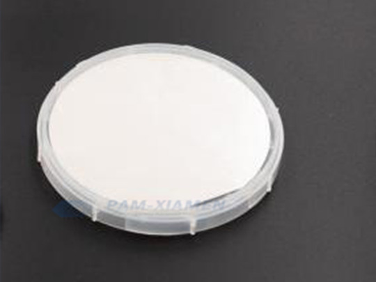
SAPPHIRE WAFERS / SAPPHIRE SUBSTRATES
https://www.cryscor.com/products/sapphire-wafers-sapphire-substrates/

Due to the less mismatched lattice and stable chemical and physical properties, sapphire(Al2O3) wafer is the popular substrates for III-V nitrides, superconductor and magnetic epi-film. They are widely used in GaN and thin-film epitaxial growth, silicon on sapphire, LED market and optics industry.
CRYSCORE is a professional sapphire wafer supplier who manufactures 99.999% high purity single crystal polished sapphire wafers for epitaxy. And our sapphire (Al2O3) substrates feature excellent surface finish, which is the key LED parameter.
If you are looking for reliable sapphire wafer suppliers, contact us now.
FEATURES OF SINGLE CRYSTAL SAPPHIRE
1. Sapphire has a high optical transmittance, so it is widely used as microelectronic tube dielectric material, ultrasonic conduction element, waveguide laser cavity and other optical elements, as window materials for infrared military devices, space vehicles, high-intensity lasers and optical communications...
2. Sapphire has high rigidity, high strength, high working temperature, abrasion resistance, corrosion resistance characteristics, so it is often used in harsh environments, such as boiler water gauge (high-temperature resistance), commodity bar code scanner, bearing and other precision manufacturing (wear resistance), coal, gas, well detection sensors and detector windows (anti-corrosion)...
3. Sapphire has the characteristics of electrical insulation, transparency, good thermal conductivity and high rigidity, so it can be used as the substrate material of integrated circuits, such as LED and microelectronic circuits, ultra-high-speed integrated circuit.
CRYSCORE'S EXCELLENT SAPPHIRE WAFERS
99.999 % high purity single crystal Al2O3 material.
Special CMP (Chemical Mechanical Polishing) technology to ensure its performance at a low cost.
Excellent surface quality in all orientations (less than 0.2 nm for C-plane, less than 0.5 nm for A-plane, M-plane, R-plane, N-plane, V-plane, 10-14, etc.)
Cleaned in class 100 cleanroom by ultrapure water with quality above 18MΩ *cm.
25 pcs a pack or single pack is available to maximize customer flexibility in their research.
Traceable product serial number.
Compact carton packaging for safer shipping and cost-saving.
Standard wafers are Generally in stock to ensure a quick delivery.
LOOK AT WHERE SAPPHIRE WAFER APPLIED
1. Semiconductor LED industry (MOCVD epitaxial GaN substrate)
In general, C-plane sapphire is needed in this area. R-plane or M-plane mainly used to grow non-polar/semi-polar plane epitaxial layers to improve the luminescence efficiency.
2. The growth of III-V or II-VI compound semiconductor.
3. Microelectronic IC applications especially Very High-Speed Integrated Circuit, SOS
Generally, it is a silicon heteroepitaxial deposition on R-plane sapphire.
4. Hybrid microelectronics
Hybrid microelectronics products are mainly HIC and MCM. It has high requirements on the substrate, while sapphire's characteristics such as stable dielectric constant and low dielectric loss make sapphire wafer the most commonly used substrate for HIC and the main substrate for MCM. Generally, the A-plane sapphire wafer is needed.
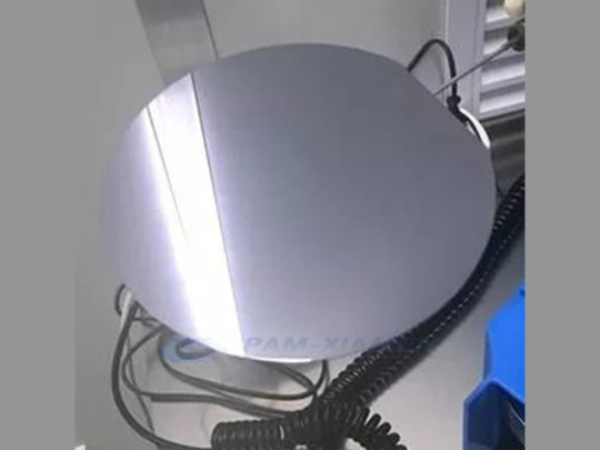
SAPPHIRE WAFER PROCESSING
At the very beginning, we have a crystal boule.
Crystal growing: Produce high-quality sapphire monocrystals via furnace.
Sapphire ingot processing: Drill out the ingot, Ground the ingot, Quality inspection.
Then we get the sapphire ingot.
Orientation: Position the ingot on the sawing machine.
Sawing: Cut the ingot into thin wafers.
Lapping: Lap the wafer to remove the scratched layer and improve its flatness.
Chamfer: Trim the edge of the wafer into an arc to improve the mechanical strength, to avoiding stress concentration.
Polishing: Reduce the surface roughness to reach the epitaxial wafer grade.
Cleaning: Remove dirt from the wafer surface.
Quality inspection: Inspect wafer with a high precision instrument to meet customer's requests.
Finally, we get the sapphire wafer.
0 notes
Text
Get to Know Which Substrate is better for GaN Template
Get to Know Which Substrate is better for GaN Template
Today every device has begun to network as a result there is a need for speed that is ultimately pushing the industry toward 5G. It is the next-generation telecom standard that promises to give greater bandwidth and reduced latency. Many 5G bands are based on the frequency bands that are quite challenging for traditional semiconductor devices that are based on silicon GaN Epi on…
View On WordPress
#GaN epi on sapphire china#GaN epi on sapphire wafer#GaN epi on sapphire wafer manufacturer#GaN epi wafer on sapphire
1 note
·
View note
Last Seen Blogs

intimages
IntImages.Biz


vrgx
Ravengambitx Nerd Blog


orca-iguana
Is that a trilobite 👀 💖 you are friend now.