#High Temperature PCB Tags
Explore tagged Tumblr posts
Visit Tumblr Blog
Explore Tumblr blogs with no restrictions, modern design and the best experience.
Last Seen Tumblr Blogs


Fun Fact
The average Tumblr user visits about 67 pages every month.
Text
Every construction company faces the challenge of cutting costs without compromising efficiency. With tight budgets, project delays, and the constant risk of theft, staying on track can feel like an uphill battle. But what if there was a way to streamline operations, prevent losses, and keep your projects running like clockwork? That’s where RFID technology steps in. This advanced tracking solution has become a game-changer for the construction industry, helping companies stay within budget and improve how they manage their resources.
RFID technology is gaining rapid popularity due to its ability to solve some of the most persistent problems in construction. By Using RFID tags to track inventory in real time to reduce downtime caused by missing equipment, RFID brings precision and efficiency to construction site management. Implementing RFID technology allows for better coordination between workers and materials, reducing delays and minimizing errors. This not only helps to control costs but also keeps projects moving forward smoothly.
Our PCB RFID Tags are highly reliable, durable, with anti-counterfeit technology, and absolutely compatible with high temperatures comparatively. These are also known as smart PCBs with RFID tags. The working remains the same and can be easily deployed for all types of tracking. These tags are so small that they can be easily embedded with electronic equipment like Mobile Phones, LEDs, Computers, and other electronic devices that contain a PCB. Apart from this, these can also be used in consumer goods, medicines, straps and medical equipment, Metallic Molds, Hardware tools, etc. These tags have their own advantages as they need very low space on the PCB, can work easily without an antenna, and can also communicate without a line-of-sight connection possible.
If you have questions about any of our RFID Tags listed below please feel free to contact us.
#RFID Tags#RFID Technology#rfid solutions#Construction Sites#Inventory Management#Asset Tracking#High Temperature PCB Tags#RFID asset Tags#RFID Metal tags
0 notes
Text
Flexographic Electronics: The Fastest Growing Segment in Printed Tech

Flexographic printing technology employs flexible relief plates to directly print functional inks such as PEDOT/PSS, silver-based, and dielectric formulations onto substrates ranging from plastics and metals to paper and fabrics. While historically focused on packaging labels, bags, and flexible pouches, recent innovations have extended its scope into electronics. Applications now include organic thin-film transistors (OTFTs), photovoltaic cells, electrochromic displays, wearable sensors, and more. In 2023, the global Flexography Printed Electronics market was valued at US$ 1.9 Bn, and is projected to reach US$ 5.9 Bn by 2034, growing at a robust 10.9% CAGR over the forecast period.
“Expansion of the consumer electronics industry and the surge in demand for environmentally friendly printing solutions are expected to propel the Flexography Printed Electronics Market to new heights,” says lead analyst at Global Industry Research. “With a forecasted CAGR of 10.9% from 2024 through 2034, the market presents a lucrative opportunity for new entrants to establish manufacturing facilities and drive technological advancement. Flexography’s adaptability and cost efficiency have made it the preferred choice across diverse applications beyond traditional packaging, reinforcing its critical role in the broader printed electronics ecosystem. Asia Pacific, buoyed by rapid adoption in consumer electronics, is poised to lead global growth.”
Market Drivers & Trends
Surge in Adoption of Conductive Inks: Manufacturers are increasingly embracing silver-based and other conductive inks to replace traditional PCB techniques, reducing production costs and simplifying supply chains. Conductive inks facilitate rapid prototyping and mass manufacturing of printed circuitry for sensors, RFID tags, and flexible interconnects.
Smart Packaging Integration: The demand for smart packaging featuring printed sensors for temperature, humidity, and freshness monitoring, as well as printed RFID/QR codes for authentication and inventory tracking is accelerating. Flexography’s high-throughput capabilities and low per-unit cost make it ideal for embedding electronics into mainstream packaging.
Environmental and Cost Efficiency: Silver conductive inks have eclipsed gold and platinum alternatives by offering a more affordable, scalable solution. Flexography’s relatively low solvent usage and compatibility with eco-friendly substrates further enhance its environmental credentials.
Latest Market Trends
Flexible, Rollable Displays: Flexography-printed displays for e-readers, tablets, wearables, and automotive heads-up displays are garnering strong interest. Manufacturers can now produce bendable, durable screens that maintain clarity and performance under repeated flexing.
In-Mold Electronics (IME): Integration of printed electronics into molded plastic parts such as smart device housings and automotive interiors is on the rise. IME enables seamless, lightweight integration of sensors and antennas.
Organic Electronic Materials: Advances in organic semiconductive and dielectric inks are unlocking novel applications in OLED lighting, organic photovoltaic films, and bio-sensors, offering low-temperature processing and roll-to-roll manufacturing compatibility.
Key Players and Industry Leaders
The Flexography Printed Electronics market remains fragmented, characterized by numerous specialized providers investing heavily in R&D and strategic partnerships. Notable players profiled in the latest report include:
Alstom SA
Brückner Maschinenbau GmbH & Co. KG
DuraTech Industries
Heidelberger Druckmaschinen AG
Henkel AG & Co. KGaA
InkTec Co., Ltd
Jabil Inc.
KOMURA-TECH CO., LTD.
Molex, LLC.
Nissha Co., Ltd
TRITEK CO.,LTD
Witte Technology GmbH
Other Key Players
New/ Emerging Players
Recent Developments
Henkel’s Bridgewater Adhesive Technologies Center (May 2023): Opened in the U.S., this hub focuses on printed electronics innovations for applications spanning hygiene products to engineered wood, fostering collaboration across more than 800 industry segments.
XSYS nyoflex FTV Plate Launch (March 2023): The company introduced a digital photopolymer plate designed for high-efficiency plate production and superior print quality with solvent-based inks, targeting flexible packaging and printed electronics sectors.
Examine key highlights and takeaways from our Report in this sample - https://www.transparencymarketresearch.com/sample/sample.php?flag=S&rep_id=86362
Market Opportunities
Entry of New Manufacturers: The market’s high growth trajectory and relatively low capital barriers present an ideal window for startups and regional players to invest in flexographic printing capacities and carve out niche segments.
Technological Innovation: Breakthroughs in ink formulation particularly in eco-friendly, water-based conductive inks offer differentiation opportunities. Co-development partnerships between ink formulators and press manufacturers can yield turnkey solutions tailored for electronics applications.
Adjacent Industry Adoption: Increased integration of printed electronics in medical wearables, industrial sensors, and aerospace components opens new verticals beyond packaging and consumer electronics.
Future Outlook
Over the next decade, the Flexography Printed Electronics market is expected to benefit from:
Advancements in Roll-to-Roll Manufacturing: Higher line speeds and improved process controls will reduce unit costs and enhance print resolution, enabling complex circuitry fabrication.
Smart Textiles and Wearables: Printed flexible batteries, textile-integrated sensors, and conductive threads will drive demand in health monitoring and fitness markets.
Automotive Electronics: As vehicles incorporate more distributed sensors for safety and connectivity, flexo-printed antennas, heaters, and interface films will gain prominence.
Market Segmentation
Material:
Substrates: Polymers, Papers, Fabrics, Silicon, Glass, Metals
Inks: Conductive, Dielectric, Semiconductive
Application:
Sensors & Switches, Displays, Medical Wearables, Photovoltaic Cells, Antennas, Heaters, In-Mold Electronics, Lighting, Others
Industry Vertical:
Automotive & Transportation, Consumer Electronics, Healthcare, Aerospace & Defense, Industrial, Others
Regional Insights
Asia Pacific (41.1% share, 2023): Dominant region driven by large-scale consumer electronics manufacturing in China, South Korea, and Japan. Government initiatives in smart cities and electric vehicles further bolster demand.
North America: Growth fueled by smart packaging uptake in food and pharmaceuticals, and strong R&D ecosystem for printed electronics in the U.S. and Canada.
Europe: Adoption across automotive, healthcare, and packaging sectors, with Germany and the U.K. leading in process innovation and regulatory support for sustainable manufacturing.
Middle East & Africa / Latin America: Emerging markets exhibit steady growth as packaging converters upgrade facilities and multinationals extend regional footprints.
Frequently Asked Questions
1. What is the projected market size of Flexography Printed Electronics by 2034? The market is forecast to grow from US$ 1.9 Bn in 2023 to US$ 5.9 Bn by the end of 2034, representing a CAGR of 10.9%.
2. Which region leads the market? Asia Pacific dominated the market in 2023 with a 41.1% share, driven by massive consumer electronics manufacturing in China, South Korea, and Japan.
3. What are the key drivers of growth? Primary drivers include the adoption of cost-effective conductive inks, demand for smart packaging solutions, growth in flexible displays, and the push for sustainable manufacturing practices.
4. Who are the leading players in this industry? Key players include Henkel AG & Co. KGaA, Heidelberger Druckmaschinen AG, Molex, LLC, Nissha Co., Ltd, InkTec Co., Ltd, among others that hold significant market share and lead in innovation.
5. What future trends will impact the market? Trends such as roll-to-roll high-speed manufacturing, smart textiles, automotive printed sensors, and advanced organic inks will shape market growth through 2034. About Transparency Market Research Transparency Market Research, a global market research company registered at Wilmington, Delaware, United States, provides custom research and consulting services. Our exclusive blend of quantitative forecasting and trends analysis provides forward-looking insights for thousands of decision makers. Our experienced team of Analysts, Researchers, and Consultants use proprietary data sources and various tools & techniques to gather and analyses information. Our data repository is continuously updated and revised by a team of research experts, so that it always reflects the latest trends and information. With a broad research and analysis capability, Transparency Market Research employs rigorous primary and secondary research techniques in developing distinctive data sets and research material for business reports. Contact: Transparency Market Research Inc. CORPORATE HEADQUARTER DOWNTOWN, 1000 N. West Street, Suite 1200, Wilmington, Delaware 19801 USA Tel: +1-518-618-1030 USA - Canada Toll Free: 866-552-3453 Website: https://www.transparencymarketresearch.com Email: [email protected]
0 notes
Text
CHIP Ceramic Patch Antenna vs. Bluetooth Patch Antenna: Which Is More Suitable for Your Device?
In wireless communication device design, antenna selection directly impacts signal transmission quality, device size, and user experience. With the rapid development of fields like the Internet of Things (IoT) and smart wearables, CHIP ceramic patch antennas and Bluetooth patch antennas have become mainstream choices due to their distinct characteristics.

I. Antenna Basics: CHIP Ceramic Patch Antenna vs. Bluetooth Patch Antenna
1. CHIP Ceramic Patch Antenna
Principle and Structure:Utilizes ceramic materials (such as dielectric ceramics) as the substrate, achieving signal transmission and reception through microstrip or radiation patch designs. The high dielectric constant of ceramics allows the antenna to operate at smaller sizes, suitable for high-frequency applications (e.g., 2.4GHz, 5GHz).
Core Advantages:
Multi-Band Compatibility: Supports Wi-Fi, Bluetooth, Zigbee, and other protocols, reducing the number of antennas within a device.
Strong Environmental Resistance: Ceramic material is resistant to high temperatures and corrosion, making it suitable for industrial or outdoor scenarios.
High Signal Purity: Low-loss characteristics reduce signal interference, enhancing transmission stability.
2. Bluetooth Patch Antenna
Principle and Structure:Specifically designed for the Bluetooth frequency band (2.4GHz-2.485GHz), typically using PCB substrates or flexible materials. The structure is simple, and the cost is relatively low.
Core Advantages:
Extreme Miniaturization: Sizes can be as small as 3×1.5mm, suitable for miniature devices (e.g., TWS earbuds).
Low Power Consumption Optimization: Designed for Bluetooth Low Energy (BLE) protocols, extending battery life.
Rapid Integration: No complex matching circuits required, simplifying the development process.
II. Key Comparisons: Which Is More Suitable for Your Device?
Comparison DimensionCHIP Ceramic Patch AntennaBluetooth Patch AntennaApplicable Frequency BandsMulti-band (Wi-Fi/Bluetooth/Zigbee, etc.)Single Bluetooth bandSizeRelatively larger (considering ceramic substrate thickness)Extremely small (suitable for space-constrained devices)CostHigher (due to material and process complexity)Lower (standardized design)Environmental AdaptabilityExcellent (resistant to high temperatures, vibrations)General (depends on PCB protection)Typical ApplicationsSmart home gateways, industrial sensors, smartwatchesBluetooth earbuds, smart tags, medical wearables
Scenario-Based Selection Recommendations
Need Multi-Protocol Support? Choose CHIP Ceramic Patch AntennaFor example, smart home central control devices need to connect to both Wi-Fi and Bluetooth. The multi-band characteristics of ceramic antennas can reduce the number of antennas, optimizing layout.
Kinghelm Case: Their KH-CPA series ceramic antennas support dual-band (2.4GHz/5GHz), applied in smart speakers, enhancing signal coverage by 20%.
Pursuing Extreme Miniaturization? Choose Bluetooth Patch AntennaFor instance, TWS earbuds have limited internal space, making the miniature design of Bluetooth patch antennas an ideal choice.
Kinghelm Case: The KH-BTA series patch antennas measure only 3.2×1.6mm, enabling a brand's earbuds to achieve stable transmission over 10 meters.
Operating in Harsh Environments? Choose Ceramic AntennaIndustrial equipment operating in high-temperature or vibration environments benefits from the high reliability of ceramic materials.
Kinghelm Technical Highlight: Achieved AEC-Q200 automotive-grade certification, withstanding temperatures ranging from -40℃ to 125℃.
III. Kinghelm Solutions: Technology and Services
As a leading domestic supplier of microwave RF antennas, Kinghelm Electronics offers customized antenna solutions for various scenarios:
1. CHIP Ceramic Patch Antenna
KH-CPA Series:
Supports multiple frequency bands, compatible with major global communication protocols.
Uses environmentally friendly ceramic materials, compliant with RoHS standards.
Application Areas: Smartwatches, industrial IoT terminals.
2. Bluetooth Patch Antenna
KH-BTA Series:
Transmission power up to +4dBm, reception sensitivity -96dBm.
Supports Bluetooth 5.2/5.3, with a transmission rate of 2Mbps.
Application Areas: Medical monitoring devices, asset tracking tags.
3. Value-Added Services
Free Simulation Design: Optimize antenna radiation direction based on device structure.
Rapid Prototyping: Provide samples within 5 working days, accelerating product launch.
Global Certification Support: Assist in obtaining FCC, CE certifications, reducing compliance risks.
IV. How to Scientifically Choose an Antenna? 3 Steps
Clarify Requirements: Which frequency bands does the device support? Is multi-protocol compatibility needed?
Assess Environment: What are the operating temperature, humidity, and electromagnetic interference levels?
Balance Costs: With limited budget, prioritize standardized Bluetooth antennas; for high-performance needs, investing in ceramic antennas is worthwhile.
V. Conclusion
Both CHIP ceramic patch antennas and Bluetooth patch antennas have their merits. The key to selection lies in matching the specific needs of the device. Whether pursuing multi-band compatibility or focusing on Bluetooth performance, Kinghelm Electronics offers cost-effective solutions. Their products not only lead in technology but also earn global customer trust.
About Kinghelm
Kinghelm is a leading provider of high-quality electronic components, including RoHS-compliant antennas, wires, plug-ins, switches, and connectors. With over 17 years of experience, the company serves industries including automotive, telecommunications, industrial automation, medical devices, and consumer electronics. Kinghelm is known for its durable, reliable components that meet international standards and are used in applications ranging from renewable energy to IoT devices.
0 notes
Text
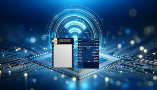
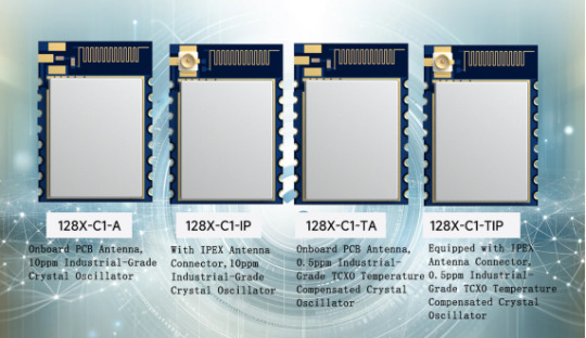
LoRa128X-C1 Series: High Sensitivity 2.4GHz, IPEX/PCB antenna, Long Range LoRa Modules
The LoRa128X-C1 series is a set of advanced modules designed to meet the diverse needs of modern wireless communication applications. Users can choose from four different models - LoRa128X-C1-TIP, LoRa128X-C1-IP, LoRa128X-C1-TA, and LoRa128X-C1-A - to select the module that best suits their specific requirements.
Applications :
The LoRa128X-C1 series is highly suitable for a wide range of applications, including wireless remote controls, smart home devices, toy control, tire pressure monitoring, health monitoring, and tag readers and writers.
Model Overview:
LoRa128X-C1-A: Features an onboard PCB antenna and a 10ppm industrial-grade crystal oscillator, providing a balance between performance and economy.
LoRa128X-C1-IP: Equipped with an IPEX antenna base and a 10ppm industrial-grade crystal oscillator, offering high cost-effectiveness and efficient operation.
LoRa128X-C1-TA: Comes with an onboard PCB antenna and a 0.5ppm industrial-grade TCXO, ensuring reliable and accurate communication.
LoRa128X-C1-TIP: Features an IPEX antenna base and a 0.5ppm industrial-grade TCXO temperature-compensated crystal oscillator, ensuring precise and stable performance.
Main features:
Operating frequency range: 2400-2500 MHz.
Modulation modes: LoRa, FLRC, and FSK modulation.
Data transfer rate: 0.476-202 Kbps under LoRa modulation.
Maximum Output power: 12.5dBm.
Sensitivity: -132dBm under LoRa modulation.
Accuracy: High precision crystal oscillator (0.5ppm TCXO/10ppm).
Communication: Packet communication mode, with 256 bytes of receive and transmit FiFo.
Operating Voltage range: 1.8-3.7 V.
Operating Temperature range: -40 to +85°C.
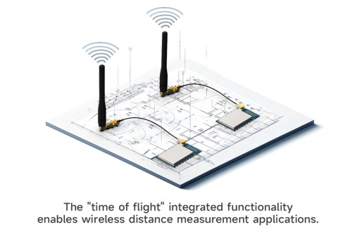
The LoRa128X-C1 series LoRa modules are produced and tested using lead-free processes, compliant with RoHS and REACH standards, ensuring not only environmental friendliness but also high quality and reliable performance. Based on Semtech's original SX1280/SX1281 RF chip, these modules utilize LoRa modulation to overcome the limitations of traditional 2.4GHz modules in terms of communication distance. Additionally, they integrate the "time of flight" function for wireless distance measurement applications.
With the high penetration performance of the 2.4GHz frequency band and LoRa mode, the LoRa128X-C1 series has very high receiving sensitivity and strong environmental anti-interference capability, making it very suitable for situations requiring long-distance 2.4GHz transmission. Choose the LoRa128X-C1 series LoRa modules as part of your next project and experience the excellent performance and versatility it offers in the field of wireless communication.
For details, please click:https://www.nicerf.com/products/ Or click:https://nicerf.en.alibaba.com/productlist.html?spm=a2700.shop_index.88.4.1fec2b006JKUsd For consultation, please contact NiceRF (Email: [email protected]).
0 notes
Text

What is Rogers PCB?
Rogers PCB is a type of printed circuit board (PCB) material made from a combination of epoxy and ceramic. It is well known for its high dielectric constant, low loss tangent, and high thermal conductivity, making it an ideal material for high-frequency applications. It is used in a wide range of electronics, such as:
5G Station
Cellular Base Station Antennas and Power Amplifiers
Automotive Radar and Sensors
Microwave point to point (P2P) links
LNB’s for Direct Broadcast Satellites
Microwave equipment of all kinds.
RF Identification (RFID) Tags
Rogers PCB is produced using the raw materials of the Rogers Company. Rogers company manufactures the laminate materials that are often used for manufacturing circuit boards. The Rogers PCB is a type of high-frequency PCB board, quite different from the traditional PCB board materials, epoxy resin. It uses the ceramic base as the material of high frequency. The major advantage of Rogers PCB is the temperature stability and superior dielectric constant.
Rogers PCB has a major application in high-speed electronic designs, radio frequency applications, and commercial microwaves. The low water absorption capacity of this Rogers PCB is ideal for the application of high humidity. Other Rogers PCB applications include RF identification tags, power amplifiers, automotive radar, sensors, etc.
Rogers PCB fabrication needs in-depth research on high-frequency PCB. HITECHPCB is a Rogers PCB manufacturer and has a deep understanding of the performance of Rogers PCB material. For example, Rogers PCB laminates and Rogers PCB dielectric constant in Rogers PCB material properties Rogers PCB is a high-frequency PCB material model produced by Rogers company, different from the conventional FR-4 PCB material. There is no epoxy resin in the Rogers PCB material, and Rogers ceramic PCB is used as the High-frequency PCB material. Absorption of Rogers PCB, it can be used as an ideal choice for application ns in high humidity environments, providing customers in the high-frequency PCB industry with the highest quality.
Difference Between Rogers Materials and FR-4 Materials
By combining Rogers PCB layers with FR-4 layers, we can achieve reduced cost and maximum performance compared to if we used only Rogers layers. Thus, this process should use Rogers PCB cores instead of prepregs for this process.
FR-4 stack up with 6 layers is shown below. Because prepreg is less expensive than cores, it is placed on the outside to minimize cost. A foil build is often referred to as this.
Rogers layers are required on the outside layers, but the core is usually found on the layers that need them. Below is an example with 6 layers but with 3 cores instead of 2. This configuration is sometimes called a "core build" or "cap construction" board. Rogers PCB is a high-frequency circuit board that has ceramic laminates and reinforced hydrocarbon. A Rogers PCB may be made from cores and prepregs, but most often, the top two copper layers are carried on the core, while the rest of the board is made from standard FR-4 to reduce the cost. The PCB materials absorb the signal, due to which it has less signal loss compared to that of FR-4. At higher frequencies, the signal loss is greater in FR-4 materials. This is also the signal length and design dependent.
High-Frequency
PCB with FR-4 materials is preferred due to their low cost, reliability, and well-understood electrical and mechanical properties. They are used in various applications ranging from microwave designs to audio circuits. Unfortunately, FR-4 printed circuit boards are not suitable for high-frequency applications. Rogers created the most well-known high-frequency-special laminates. Its materials have a constant dielectric reduction of close to 20% when compared to FR-4 printed circuit boards.
The best way to determine whether your project will benefit from high-frequency laminates is to assess electrical and mechanical requirements. If you find both variations are too broad, Rogers PCB material is a better option.
Dissipation
The material used is most important when producing printed circuit boards, though it may require a high cost. However, it is not the only issue that knows the content value when it comes to the loss factor or Df. FR-4 printed circuit boards will be affected or reduced. The losses are greater when compared to printed circuit boards made from Rogers materials.
In other words, when compared to Rogers PCB, FR-4 materials have a higher dissipation factor, especially at high frequencies. Typical values for FR-4 printed circuit boards are around 0.020 and close to 0.004 for Rogers boards. Dissipation of FR-4 materials increases with frequency. High-frequency laminates primarily have a frequency-dependent stable dissipation characteristic.
The signal loss is minimized with the lower dissipation factor in FR-4. Also, the automated assembly process and the processing of FR-4 materials make them easier in the assembly and manufacturing process.
Impedance Stability
Impedance is the measure of the current opposition when applying voltage. In many design applications, the stable impedance is essential and is an area where the materials like Rogers and FR-4 are applied.
FR-4, despite its low cost, is prone to high variations in the dielectric constant with the change in temperature across the length and width of the substrate. In terms of impedance stability, Rogers' material has a wider range of dielectric constants than FR-4 content.
High-frequency laminates are preferable for circuits that require little variation over wide temperature ranges. In this case, you may need to use printed circuit boards made of Rogers materials rather than FR-4 materials, especially if most of your operations involve working in high-temperature environments.
Dielectric Constant
The dielectric constant of any material measures a substance's ability to store some electrical energy across an electrical field. When it comes to dielectric constant, FR-4 has a dielectric constant of about 4.5, which is much lower than Roger's material, which has a dielectric constant of about 6.15 to 11.
The dielectric constant of FR-4 is comparatively higher than that of plastic materials. Using FR-4 materials can save at least 25% of PCB made from such materials. Other factors that make FR-4 articles available include their lightweight, moisture resistance, and high dielectric strength. Even though the Rogers PCB has a higher dielectric than FR-4, you can go with FR-4. FR-4 and Rogers 4350b and 4350 are similar manufacturing processes, although FR-4 stores electrical energy effectively.
Thus, PCB with higher dialect trends breaks easier when subjected to intense electric fields.
0 notes
Photo


PCB material UHF Anti Metal Tag, ABS material UHF Anti Metal Tag, Ceramic Material High Temperature UHF Anti-metal Tag. Multiple specifications, accept custom size specifications, frequency. http://www.seabreezerfid.com/rfid-dedicated-tag/rfid-anti-metal-tag Focus on Seabreeze Smart Card Co., Ltd. Website: http://www.SeabreezeRFID.com/ Sales contact: [email protected]
#PCB material UHF Anti Metal Tag#ABS material UHF Anti Metal Tag#ABS material Anti Metal Tag#Ceramic Material High Temperature UHF Anti-metal Tag#UHF Ceramic Material High Temperature Anti-metal Tag#Seabreeze Smart Card Co. Ltd#SeabreezeRFID#SeabreezeRFID Co.Ltd.
1 note
·
View note
Text
RFID PCB Tags | UHF RFID PCB Tags | PCB RFID Tag Manufacturer-India

ID Tech Solutions Manufacturer, Provider Of RFID PCB Tags, HF & UHF, Printed Circuit Board RFID Tags, Easily Traceable, Durable, Anti Counterfeit Smart PCB Tag, Buy At Best Price In India, Gurgaon, Delhi, High Temperature Tags, Logistics and Production Tracking Tags, Tags For Inventory Control and Product Authenticity, Small PCB Tags
1 note
·
View note
Text
Conductive Inks Market Is Expected To Reach New Growth Revenues During 2021-2028
Global Conductive inks market is anticipated to witness significant growth over the forecast period. Research initiatives to develop cost-effective raw materials, such as copper, nickel, and grapheme, which have properties similar to that of silver, are projected to further aid in the market growth in the near future. The research initiatives undertaken by both government and industry participants and are expected to increase multiple potential applications, which in turn are projected to complement the global conductive inks market growth.
Conductive inks have excellent electron mobility, high conductivity & low resistivity, as well as high thermal & chemical stability. These inherent properties contribute to increased efficiency of conductive ink applications such as PCB boards, RFID tags printing, and circuit repairing. Furthermore, the particle size of conductive inks can be adjusted to suit the requirements of the application. Increasing need for customization coupled with favorable properties of conductive inks suitable for electronic application needs is expected to aid in the overall market growth.
New product types, which suit rigid as well as flexible substrates and can achieve low electrical resistivity, have been developed. These developments are expected to benefit the conductive inks market globally. Inks requiring low curing temperature and having anti-shrinking properties were also launched in the past.
The electronics market is highly competitive in nature, and, therefore, key market players are constantly attempting to miniaturize their product offerings. Miniaturization involves the manufacturing of optical, mechanical, and electronics products to achieve product differentiation. Conductive inks are used to produce electrical contacts, short network connection, and improved layout design, which aids in miniaturization. These require single-sided assembly and resistance is created at the same time. The need for miniaturization is anticipated to grow over the forecast period due to the rising competition in regional markets such as in the Asia Pacific & Europe regions.
Download sample: https://www.polarismarketresearch.com/industry-analysis/conductive-inks-market/request-for-sample
They are used for manufacturing printed circuit boards, which are widely employed in automotive components. They are used to coat assemblies and components to shield them from radio interference. Car seat heaters and window defoggers use them for circuit tracing. Various companies are trying to develop interactive displays for achieving product differentiation. For instance, Henkel is involved in the manufacturing of fully printed ink products such as silver inks, dielectric inks, transparent, and bendable resistive inks, which are primarily used for electronic assembly purposes.
Silver inks are widely being used in electronic application owing to their excellent conductibility and printability. However, manufacturers have come up with alternative solutions that exhibit properties similar to that of silver due to the scarce availability of raw materials and high costs of silver inks. Copper has been identified as a good alternative for silver due to its low cost and high electrical conductivity. Therefore, due to these properties, manufacturers can reduce the production cost of conductive inks.
Companies such as Henkel have introduced conductive inks containing minimal silver formulations. The conductive ink produced by Henkel LOCTITE ECI 1001 E&C, finds use in the automotive sensor application, as customers demand a low-cost alternative of conductive silver inks. The product, which delivers the same performance as traditional conductive silver inks, is inexpensive and contains lesser silver content.
Get Discount offer: https://www.polarismarketresearch.com/industry-analysis/conductive-inks-market/request-for-discount-pricing
Polaris Market Research has segmented the global conductive inks market on the basis of products, application and region: Conductive Inks Product Outlook (Revenue, USD Million, 2015 – 2026)
Conductive Silver Ink
Conductive Copper Ink
Conductive Polymer
Carbon Nanotube Ink
Dielectric Ink
Carbon/Graphene Ink
Conductive Inks Application Outlook (Revenue, USD Million, 2015 – 2026)
Photovoltaic
Membrane Switches
Displays
Automotive
Smart Packaging/RFID
Biosensors
Printed Circuit Boards
Conductive Inks Regional Outlook (Revenue, USD Million, 2015 – 2026)
North America
Europe
Asia-Pacific
Latin America
Middle East and Africa
U. S.
Canada
Germany
UK
France
Spain
Russia
Rest of Europe
China
India
Japan
Australia
Singapore
Korea
Rest of Asia-Pacific
Brazil
Mexico
Argentina
Rest of Latin America
UAE
Saudi Arabia
South Africa
Rest of MEA
Buy Now: https://www.polarismarketresearch.com/checkouts/5341
0 notes
Text
Conductive Inks Market To Witness Massive Growth During Forecast Period
Global Conductive inks market is anticipated to witness significant growth over the forecast period. Research initiatives to develop cost-effective raw materials, such as copper, nickel, and grapheme, which have properties similar to that of silver, are projected to further aid in the market growth in the near future. The research initiatives undertaken by both government and industry participants and are expected to increase multiple potential applications, which in turn are projected to complement the global conductive inks market growth.
Conductive inks have excellent electron mobility, high conductivity & low resistivity, as well as high thermal & chemical stability. These inherent properties contribute to increased efficiency of conductive ink applications such as PCB boards, RFID tags printing, and circuit repairing. Furthermore, the particle size of conductive inks can be adjusted to suit the requirements of the application. Increasing need for customization coupled with favorable properties of conductive inks suitable for electronic application needs is expected to aid in the overall market growth.
Get Sample copy of this report : https://www.polarismarketresearch.com/industry-analysis/conductive-inks-market/request-for-sample
New product types, which suit rigid as well as flexible substrates and can achieve low electrical resistivity, have been developed. These developments are expected to benefit the conductive inks market globally. Inks requiring low curing temperature and having anti-shrinking properties were also launched in the past.
The electronics market is highly competitive in nature, and, therefore, key market players are constantly attempting to miniaturize their product offerings. Miniaturization involves the manufacturing of optical, mechanical, and electronics products to achieve product differentiation. Conductive inks are used to produce electrical contacts, short network connection, and improved layout design, which aids in miniaturization. These require single-sided assembly and resistance is created at the same time. The need for miniaturization is anticipated to grow over the forecast period due to the rising competition in regional markets such as in the Asia Pacific & Europe regions.
They are used for manufacturing printed circuit boards, which are widely employed in automotive components. They are used to coat assemblies and components to shield them from radio interference. Car seat heaters and window defoggers use them for circuit tracing. Various companies are trying to develop interactive displays for achieving product differentiation. For instance, Henkel is involved in the manufacturing of fully printed ink products such as silver inks, dielectric inks, transparent, and bendable resistive inks, which are primarily used for electronic assembly purposes.
Silver inks are widely being used in electronic application owing to their excellent conductibility and printability. However, manufacturers have come up with alternative solutions that exhibit properties similar to that of silver due to the scarce availability of raw materials and high costs of silver inks. Copper has been identified as a good alternative for silver due to its low cost and high electrical conductivity. Therefore, due to these properties, manufacturers can reduce the production cost of conductive inks.
Companies such as Henkel have introduced conductive inks containing minimal silver formulations. The conductive ink produced by Henkel LOCTITE ECI 1001 E&C, finds use in the automotive sensor application, as customers demand a low-cost alternative of conductive silver inks. The product, which delivers the same performance as traditional conductive silver inks, is inexpensive and contains lesser silver content.
Polaris Market Research has segmented the global conductive inks market on the basis of products, application and region:
Conductive Inks Product Outlook (Revenue, USD Million, 2015 – 2026)
· Conductive Silver Ink
· Conductive Copper Ink
· Conductive Polymer
· Carbon Nanotube Ink
· Dielectric Ink
· Carbon/Graphene Ink
Conductive Inks Application Outlook (Revenue, USD Million, 2015 – 2026)
· Photovoltaic
· Membrane Switches
· Displays
· Automotive
· Smart Packaging/RFID
· Biosensors
· Printed Circuit Boards
Conductive Inks Regional Outlook (Revenue, USD Million, 2015 – 2026)
North America
· U. S.
· Canada
Europe
· Germany
· UK
· France
· Spain
· Russia
· Rest of Europe
Asia-Pacific
· China
· India
· Japan
· Australia
· Singapore
· Korea
· Rest of Asia-Pacific
Latin America
· Brazil
· Mexico
· Argentina
· Rest of Latin America
Middle East and Africa
· UAE
· Saudi Arabia
· South Africa
· Rest of MEA
Request For Discount : https://www.polarismarketresearch.com/industry-analysis/conductive-inks-market/request-for-discount-pricing
About Polaris Market Research
Polaris Market Research is a global market research and consulting company. The company specializes in providing exceptional market intelligence and in-depth business research services for our clientele spread across different enterprises. We at Polaris are obliged to serve our diverse customer base present across the industries of healthcare, technology, semi-conductors and chemicals among various other industries present around the world
Contact us
Polaris Market Research
Phone: 1-646-568-9980
Email: [email protected]
Web: www.polarismarketresearch.com
0 notes
Text
How RFID Tags Reduce Construction Project Costs

Every construction company faces the challenge of cutting costs without compromising efficiency. With tight budgets, project delays, and the constant risk of theft, staying on track can feel like an uphill battle. But what if there was a way to streamline operations, prevent losses, and keep your projects running like clockwork? That’s where RFID technology steps in. This advanced tracking solution has become a game-changer for the construction industry, helping companies stay within budget and improve how they manage their resources.
RFID technology is gaining rapid popularity due to its ability to solve some of the most persistent problems in construction. By Using RFID tags to track inventory in real time to reduce downtime caused by missing equipment, RFID brings precision and efficiency to construction site management. Implementing RFID technology allows for better coordination between workers and materials, reducing delays and minimizing errors. This not only helps to control costs but also keeps projects moving forward smoothly.
What is RFID Technology?
Radio Frequency Identification (RFID) technology is a system that uses electromagnetic fields to track and manage assets. RFID tags, which consist of a small chip and antenna, can be attached to tools, equipment, materials, and even employee badges. Unlike barcodes that require direct scanning, RFID tags can be read from a distance, without a line of sight. This makes gathering and tracking real-time data across a construction site easy.
From managing inventory to tracking workforce movements, RFID tags provide instant insights, allowing project managers to make better decisions. This technology is particularly useful in large construction projects where manual tracking becomes inefficient and costly.
How RFID Tags Reduce Construction Project Costs
RFID technology offers several ways to cut costs, which can make a big difference in managing a construction project efficiently. Let’s explore how RFID technology tackles some of the biggest cost-related challenges in the industry.
1. Reducing Theft
Construction site theft poses a significant problem that can substantially inflate costs. Losing expensive equipment or materials not only causes delays but also eats into the project’s budget. With an estimated annual loss between $300 million to $1 billion from theft, companies need a reliable way to protect their assets.
High Temperature RFID tags provide a layer of security that traditional methods lack. By tagging high-value tools, machinery, and building materials, construction companies can track these assets in real time. If something is moved outside a designated area, an alert is triggered, allowing immediate action to be taken. The ability to monitor equipment 24/7 not only reduces the risk of theft but also helps recover stolen items.
With RFID, companies can avoid expensive replacements and reduce insurance costs, ultimately saving significant amounts of money on projects.
2. Improving Time Management
In construction, time is money. Delays, miscommunication, and inefficiencies often lead to extra costs, especially when workers or materials aren’t where they need to be. Traditional methods of tracking labor and materials can be time-consuming and prone to human error, which can slow down projects and increase costs.
RFID technology provides real-time visibility into every aspect of a construction site. RFID tags attached to employee badges allow project managers to monitor worker attendance and location across the site. This ensures that labor is used efficiently, and workers are being paid for the exact hours they’re on the job. It also helps in tracking equipment usage, preventing any delays caused by missing tools or machinery.
Furthermore, RFID systems automate the process of tracking deliveries and inventory. This ensures that materials are delivered on time and kept in the right place, avoiding any delays or extra costs due to missing supplies. With RFID, construction managers can optimize daily operations, preventing time from slipping away and cutting down on unnecessary expenses.
3. Optimizing Resource Allocation
Efficient resource allocation is essential to keeping construction projects on budget. However, without accurate information on inventory and equipment, companies often end up over-ordering materials or renting additional machinery, leading to wasteful spending.
RFID technology offers an ideal solution for this. By providing real-time data on inventory levels, construction managers can make informed decisions about ordering materials. For example, if a certain type of building material is running low, an RFID system will send an alert before stocks are depleted. This ensures timely reordering and prevents overstocking, which reduces waste and lowers costs.
RFID tags can also track the usage of heavy machinery. If equipment is sitting idle for long periods, it might be better allocated to another site or rented out. By keeping a close eye on resource usage, construction companies can avoid the costs of renting extra machinery unnecessarily and optimize their existing assets.
The Long-Term Benefits of RFID in Construction
RFID technology doesn’t just provide immediate cost savings. It also delivers long-term benefits that can help construction companies stay competitive in the future. By improving overall site efficiency, companies can complete projects faster, minimize errors, and avoid the need for costly rework.
Beyond reducing costs, RFID systems can also help improve safety, ensure regulatory compliance, and offer better transparency throughout the supply chain. These advantages not only lead to lower costs but also contribute to better overall project outcomes.
Conclusion
RFID technology is revolutionizing the construction industry by offering practical solutions to some of the biggest cost challenges. From reducing theft to improving time management and optimizing resource allocation, RFID tags are making construction projects more efficient and cost-effective.
For companies looking to cut expenses without sacrificing quality, adopting RFID technology is a strategic move that offers both short-term savings and long-term advantages. As construction projects become more complex, RFID systems will continue to play a vital role in helping businesses stay on track and within budget.
#rfid technology#rfid solutions#rfid tags#rfid tags manufacturers#construction company#Inventory Management#High Temperature PCB Tags#RFID asset Tags#RFID Metal tags
0 notes
Text
Flexography in Healthcare: Advancing Wearable and Smart Solutions

The global Flexography Printed Electronics Market, valued at US$ 1.9 billion in 2023, is projected to grow at an impressive CAGR of 10.9% from 2024 to 2034, reaching an estimated US$ 5.9 billion by the end of the forecast period. Flexography, a highly adaptable and cost-efficient printing technology, has evolved from traditional applications to play a pivotal role in emerging sectors like consumer electronics, healthcare, and smart packaging.
Flexographic printing utilizes flexible relief plates to directly print on diverse materials such as plastics, metals, and paper. This technology has increasingly been integrated with functional materials like PEDOT/PSS, silver-based, and dielectric inks, enabling the production of advanced electronics such as organic thin-film transistors (OTFTs), photovoltaic cells, and electrochromic displays. The expanding consumer electronics industry and rising demand for environmentally friendly printing solutions are key growth drivers.
Gain a deeper perspective by visiting our detailed report - https://www.transparencymarketresearch.com/flexography-printed-electronics-market.html
Key Drivers
Surge in Adoption of Conductive Inks: The growing use of conductive inks, particularly cost-effective silver-based inks, has been a major driver in the flexography printed electronics market. These inks are being increasingly used in printed circuit boards (PCBs), replacing expensive materials like platinum and gold to reduce production costs.
Demand for Smart Packaging: Flexography printed electronics are enabling innovations in smart packaging by integrating sensors, RFID tags, and QR codes to enhance product safety, improve inventory management, and boost consumer engagement. Real-time monitoring of parameters such as temperature and freshness has augmented the adoption of printed electronics in the packaging industry.
Rising Popularity of Flexible Displays: Flexography printed electronics facilitate the production of flexible, rollable, and transparent displays, which are increasingly used in wearable devices, automotive heads-up displays, and smart windows. This segment, accounting for 31.4% of the market in 2023, is projected to expand at a CAGR of 11.9% during the forecast period.
Market Challenges and Opportunities While the market presents immense opportunities, certain challenges such as high initial costs and the need for technological advancements in manufacturing processes remain. However, the shift toward eco-friendly materials and the development of cost-efficient production techniques present lucrative opportunities for new entrants and established players alike.
The transition to solvent-based silver conductive inks is expected to revolutionize manufacturing processes, enabling faster and more cost-effective production of printed electronics.
Key Player Strategies The global flexography printed electronics market is highly fragmented, with key players such as Henkel AG & Co. KGaA, InkTec Co., Ltd, and Jabil Inc. actively focusing on:
Product Innovations: Development of advanced inks and printing techniques.
Strategic Partnerships: Collaborating with technology providers to expand market reach.
Mergers and Acquisitions: Strengthening market presence and diversifying product portfolios.
For example, in May 2023, Henkel opened an adhesive technologies center in the U.S. to advance innovations in printed electronics. Similarly, XSYS launched the nyoflex FTV Digital photopolymer plate for high-quality flexographic printing, catering to the growing demand for flexible packaging solutions.
Market Segmentation
Material: Substrates (organic and inorganic) and inks (conductive, dielectric, semiconductive).
Application: Sensors & switches, displays, medical wearables, photovoltaic cells, antennas, heaters, in-mold electronics, and lighting.
Industry Vertical: Automotive and transportation, consumer electronics, healthcare, aerospace & defense, industrial, and others.
The consumer electronics segment, accounting for 37.8% of the market in 2023, is expected to grow at a CAGR of 11.5%. Key applications include wearable devices, smart appliances, and electronic toys.
Contact:
Transparency Market Research Inc.
CORPORATE HEADQUARTER DOWNTOWN,
1000 N. West Street,
Suite 1200, Wilmington, Delaware 19801 USA
Tel: +1-518-618-1030
USA - Canada Toll Free: 866-552-3453
Website: https://www.transparencymarketresearch.com
Email: [email protected]
0 notes
Text
CHIP Ceramic Patch Antenna vs. Bluetooth Patch Antenna: Which Is More Suitable for Your Device?
In wireless communication device design, antenna selection directly impacts signal transmission quality, device size, and user experience. With the rapid development of fields like the Internet of Things (IoT) and smart wearables, CHIP ceramic patch antennas and Bluetooth patch antennas have become mainstream choices due to their distinct characteristics.
I. Antenna Basics: CHIP Ceramic Patch Antenna vs. Bluetooth Patch Antenna
1. CHIP Ceramic Patch Antenna
Principle and Structure: Utilizes ceramic materials (such as dielectric ceramics) as the substrate, achieving signal transmission and reception through microstrip or radiation patch designs. The high dielectric constant of ceramics allows the antenna to operate at smaller sizes, suitable for high-frequency applications (e.g., 2.4GHz, 5GHz).
Core Advantages:
Multi-Band Compatibility: Supports Wi-Fi, Bluetooth, Zigbee, and other protocols, reducing the number of antennas within a device.
Strong Environmental Resistance: Ceramic material is resistant to high temperatures and corrosion, making it suitable for industrial or outdoor scenarios.
High Signal Purity: Low-loss characteristics reduce signal interference, enhancing transmission stability.
2. Bluetooth Patch Antenna
Principle and Structure: Specifically designed for the Bluetooth frequency band (2.4GHz-2.485GHz), typically using PCB substrates or flexible materials. The structure is simple, and the cost is relatively low.
Core Advantages:
Extreme Miniaturization: Sizes can be as small as 3×1.5mm, suitable for miniature devices (e.g., TWS earbuds).
Low Power Consumption Optimization: Designed for Bluetooth Low Energy (BLE) protocols, extending battery life.
Rapid Integration: No complex matching circuits required, simplifying the development process.
II. Key Comparisons: Which Is More Suitable for Your Device?
Comparison DimensionCHIP Ceramic Patch AntennaBluetooth Patch AntennaApplicable Frequency BandsMulti-band (Wi-Fi/Bluetooth/Zigbee, etc.)Single Bluetooth bandSizeRelatively larger (considering ceramic substrate thickness)Extremely small (suitable for space-constrained devices)CostHigher (due to material and process complexity)Lower (standardized design)Environmental AdaptabilityExcellent (resistant to high temperatures, vibrations)General (depends on PCB protection)Typical ApplicationsSmart home gateways, industrial sensors, smartwatchesBluetooth earbuds, smart tags, medical wearables
Scenario-Based Selection Recommendations
Need Multi-Protocol Support? Choose CHIP Ceramic Patch Antenna For example, smart home central control devices need to connect to both Wi-Fi and Bluetooth. The multi-band characteristics of ceramic antennas can reduce the number of antennas, optimizing layout.
Kinghelm Case: Their KH-CPA series ceramic antennas support dual-band (2.4GHz/5GHz), applied in smart speakers, enhancing signal coverage by 20%.
Pursuing Extreme Miniaturization? Choose Bluetooth Patch Antenna For instance, TWS earbuds have limited internal space, making the miniature design of Bluetooth patch antennas an ideal choice.
Kinghelm Case: The KH-BTA series patch antennas measure only 3.2×1.6mm, enabling a brand's earbuds to achieve stable transmission over 10 meters.
Operating in Harsh Environments? Choose Ceramic Antenna Industrial equipment operating in high-temperature or vibration environments benefits from the high reliability of ceramic materials.
Kinghelm Technical Highlight: Achieved AEC-Q200 automotive-grade certification, withstanding temperatures ranging from -40℃ to 125℃.
III. Kinghelm Solutions: Technology and Services
As a leading domestic supplier of microwave RF antennas, Kinghelm Electronics offers customized antenna solutions for various scenarios:
1. CHIP Ceramic Patch Antenna
KH-CPA Series:
Supports multiple frequency bands, compatible with major global communication protocols.
Uses environmentally friendly ceramic materials, compliant with RoHS standards.
Application Areas: Smartwatches, industrial IoT terminals.
2. Bluetooth Patch Antenna
KH-BTA Series:
Transmission power up to +4dBm, reception sensitivity -96dBm.
Supports Bluetooth 5.2/5.3, with a transmission rate of 2Mbps.
Application Areas: Medical monitoring devices, asset tracking tags.
3. Value-Added Services
Free Simulation Design: Optimize antenna radiation direction based on device structure.
Rapid Prototyping: Provide samples within 5 working days, accelerating product launch.
Global Certification Support: Assist in obtaining FCC, CE certifications, reducing compliance risks.
IV. How to Scientifically Choose an Antenna? 3 Steps
Clarify Requirements: Which frequency bands does the device support? Is multi-protocol compatibility needed?
Assess Environment: What are the operating temperature, humidity, and electromagnetic interference levels?
Balance Costs: With limited budget, prioritize standardized Bluetooth antennas; for high-performance needs, investing in ceramic antennas is worthwhile.
V. Conclusion
Both CHIP ceramic patch antennas and Bluetooth patch antennas have their merits. The key to selection lies in matching the specific needs of the device. Whether pursuing multi-band compatibility or focusing on Bluetooth performance, Kinghelm Electronics offers cost-effective solutions. Their products not only lead in technology but also earn global customer trust.

About Kinghelm
Kinghelm is a leading provider of high-quality electronic components, including RoHS-compliant antennas, wires, plug-ins, switches, and connectors. With over 17 years of experience, the company serves industries including automotive, telecommunications, industrial automation, medical devices, and consumer electronics. Kinghelm is known for its durable, reliable components that meet international standards and are used in applications ranging from renewable energy to IoT devices.
0 notes
Link
If you are planning to build a gaming pc and are restricted to a budget of Rs. 40,000, then this PC build guide will help you build the best Gaming Desktop Under 40000 INR (500 USD).
For building a gaming PC, the first thing one has to consider is the budget. Because the PC components are available from low to high-end category which depends on performance and high price tag, but the less price tag components also do their job well because of the heavy competition in the gaming industries.
[su_note note_color="#7afd7d" text_color="#000000"]We may earn a commission for purchases using our links. Learn more.[/su_note] [su_note note_color="#7afd7d" text_color="#000000"]Pro Tip: Always search stores like MDComputers, VedantComputers in India and BestBuy, NewEgg, MicroCenter in the US for best pricing[/su_note]
Gaming Desktop Under 40000 INR (500 USD)
Components
These components are necessary to build a gaming PC. Let’s discuss the components which we have used to build the 40000 INR (500 USD) gaming PC.
Component Model Price Processor Ryzen 3 3100 ~ ₹ 8.6k ($ ) Motherboard MSI B450M Pro-VDH Max ~ ₹ 7.8k ($ ) RAM Corsair Vengeance 8GB DDR4 ~ ₹ 3.8k ($ 50) Hard Drive WD Blue 1TB PC Hard Drive [Optional] Crucial MX500 240GB SSD ~ ₹ 6.3k ($ ) Power Supply or PSU In-built 550 W PSU ~ N/A PC Chassis Corsair Carbide SPEC-05 with 550 W PSU ~ ₹ 6.5k ($ 85) Graphics Card Zotac GTX 1650 AMP Edition 4GB ~ ₹ 13.7k ($ )
Component Details
Let’s dive into the individual component in this system:
AMD Ryzen 3 3100 Processor
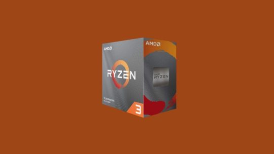
Also Read: How to Check Graphics Card Details in Windows 10?
4 Cores & 8 Threads
Base Clock: 3.6GHz, Max Boost Clock: up to 3.9GHz, 18MB Cache, TDP: 65W
System Memory Specification: 3200MHz, System Memory Type: DDR4, Memory Channels: 2
Socket: AM4, Motherboard Compatibility: AMD 300, 400, 500 series chipset-based motherboards
Graphics: Separate Graphics Card is required, Heatsink Fan: Wraith Stealth
Buy from Amazon.in
Buy from MDComputers.in
Buy from Amazon.com
Buy from NewEgg
MSI B450M Pro-VDH Max Motherboard
If you are building a gaming desktop, make sure not to compromise with the core components like Motherboard, PSU, and Processor. If you are compromising with these then you might face issues in the near future and that can cost, you a lot more while recovery.
B450M MoBos are specially designed for best gaming performance in a tight budget. These are one of the best motherboards when comes to gaming. B450M Pro-VDH Max is a soft priced motherboard from MSI. B450M Pro-M2 and B450M Pro-VDH. Both models share the same black PCB with brownish traces and tracks, while the B450M Pro-VDH makes use of a heatsink on the CPU section of the power delivery, whereas the B450M Pro-M2 omits power delivery heatsinks completely.

AMD AM4 motherboard inspired from architectural design, with Core Boost, DDR4 Boost, Audio Boost, Turbo M.2 – Supports DDR4 Memory, up to 3466+(OC) MHz.
Turbo M.2: Running at PCI-E Gen3 x4 maximizes performance for NVMe based SSDs.
DDR4 Boost: Advanced technology to deliver pure data signals for the best performance and stability.
Core Boost: With premium layout and fully digital power design to support more cores and provide better performance.
i). EZ Debug LED: The easiest way to troubleshoot. ii). PCI-E Steel Armor: Protecting VGA cards against bending and EMI.
Buy from Amazon.in
Buy from MDComputers.in
Buy from Amazon.com
Buy from NewEgg
Corsair Vengeance 8GB DDR4 RAM

Specs:
XMP 2.0 SUPPORT: One setting is all it takes to automatically adjust to the fastest safe speed for your VENGEANCE LPX kit. You’ll get amazing, reliable performance without lockups or other strange behavior.
ALUMINUM HEAT SPREADER: Overclocking overhead is limited by operating temperature. The unique design of the VENGEANCE LPX heat spreader optimally pulls heat away from the ICs and into your system’s cooling path, so you can push it harder.
DESIGNED FOR HIGH-PERFORMANCE OVERCLOCKING: Each VENGEANCE LPX module is built from a custom performance PCB and highly-screened memory ICs. The efficient heat spreader provides effective cooling to improve overclocking potential.
LOW-PROFILE DESIGN: The small form factor makes it ideal for smaller cases or any system where internal space is at a premium.
Buy from Amazon.in
Buy from Amazon.com
WD Blue 1TB PC Hard Drive

Specs:
Upgrade and backup with ease
Future-proof storage
Improve PC performance
1TB capacity
3.5-inch internal hard drive
64MB buffer size
7200 RPM Class
Buy from Amazon.in
Buy from Amazon.com
Crucial BX500 240GB SSD
By installing an SSD instead HDD can enhance not only the storage but also the speed of the processor. Your motherboard has an additional slot to accommodate the SSD. Installing this SSD will result in an enhanced performance because of the R/W speeds of 550MB/s and 520MB/s respectively. Yes, the costs of your gaming PC will exceed your budget, but you will end up with a better performing PC.
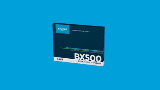
240 GB, SSD write cache is enabled, Low power consumption, Laptop, and Desktop
2.5Inch, /SATA 6 Gb/s interface, ATA modes supported
Sequential 128KB Read and Write speeds up to 540MB/s and 500MB/s respectively
Operating temperature – Commercial (0°C to 70°C)5, Voltage Input-Minimum: 4.5V, Maximum: 5.0V
Boot up faster. Load files quicker. Improve overall system responsiveness
300% faster than a typical hard drive
Improves battery life because it’s 45x more energy efficient than a typical hard drive
Buy from Amazon.in
Buy from Amazon.com
Corsair Carbide SPEC-05 Case with 550 W PSU
Specs:
Minimalist exterior design with an edge-to-edge tinted side panel window.
Room for up to five 120mm fans with one 120mm front fan pre-installed.
Expansive storage space with mounts for up to three HDD’s and two SSD’s
Clean, front panel with high-speed USB 3.0 port.
Cable routing cutouts and tie downs keep your build looking clean and uncluttered.
Removable, built-in dust filters help keep your PC clean and your components running longer.
Minimalist Exterior Design with Edge-to-Edge Side Panel Window: The asymmetrical, smooth-edged design adds bold styling to your build.
Room up to for Five 120mm Fans: Tons of room for excellent cooling potential with one 120mm front fan pre-installed.
Buy from Amazon.in
Zotac GTX 1650 AMP Edition 4GB GDDR GPU
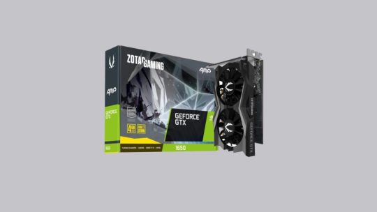
Also Read: Graphics Card Buying Guide: All You Need to Know
GPU Clock: 1725 Mhz Processors and Cores: 896 CUDA Cores Bus Standard: PCI Express 3.0 Cooling and Heatsink: Dual Slot Dual Fan Power Supply Required: 300-watt Memory: 128-bit, 4 GB GDDR5 Memory Additional Features: Turing Shaders, DirectX 12, Ansel, Fire Storm, Turing GPU Architecture
Buy from Amazon.in
Buy from Amazon.com
Buy from NewEgg
Conclusion
Well, we are almost ready with the Best Gaming Desktop Under 40000 INR or 500 USD. The Graphics Card may disturb your budget by a few bucks, but it is really worst the price. Additionally, you can later add other gaming accessories like the joystick, gaming headset, etc., for a better gaming experience.
Go through this and buy the best. If you end up buying any of these, tell us the same by commenting down below.
[su_box title="More Gaming Desktop Builds" box_color="#000000"]
Best Gaming Desktop Build Under 25000 INR (350 USD)
Best Gaming Desktop Build Under 30000 INR (400 USD)
Best Gaming Desktop Under 50000 INR (700 USD)
Best Gaming Desktop Build Under 60000 INR (800 USD)
[/su_box]
via TechLatest
0 notes
Link
Global Conductive inks market is anticipated to witness significant growth over the forecast period. Research initiatives to develop cost-effective raw materials, such as copper, nickel, and grapheme, which have properties similar to that of silver, are projected to further aid in the market growth in the near future. The research initiatives undertaken by both government and industry participants and are expected to increase multiple potential applications, which in turn are projected to complement the global conductive inks market growth.
Conductive inks have excellent electron mobility, high conductivity & low resistivity, as well as high thermal & chemical stability. These inherent properties contribute to increased efficiency of conductive ink applications such as PCB boards, RFID tags printing, and circuit repairing. Furthermore, the particle size of conductive inks can be adjusted to suit the requirements of the application. Increasing need for customization coupled with favorable properties of conductive inks suitable for electronic application needs is expected to aid in the overall market growth.
Request for sample copy of this report @ https://www.polarismarketresearch.com/industry-analysis/conductive-inks-market/request-for-sample
New product types, which suit rigid as well as flexible substrates and can achieve low electrical resistivity, have been developed. These developments are expected to benefit the conductive inks market globally. Inks requiring low curing temperature and having anti-shrinking properties were also launched in the past.
The electronics market is highly competitive in nature, and, therefore, key market players are constantly attempting to miniaturize their product offerings. Miniaturization involves the manufacturing of optical, mechanical, and electronics products to achieve product differentiation. Conductive inks are used to produce electrical contacts, short network connection, and improved layout design, which aids in miniaturization. These require single-sided assembly and resistance is created at the same time. The need for miniaturization is anticipated to grow over the forecast period due to the rising competition in regional markets such as in the Asia Pacific & Europe regions.
They are used for manufacturing printed circuit boards, which are widely employed in automotive components. They are used to coat assemblies and components to shield them from radio interference. Car seat heaters and window defoggers use them for circuit tracing. Various companies are trying to develop interactive displays for achieving product differentiation. For instance, Henkel is involved in the manufacturing of fully printed ink products such as silver inks, dielectric inks, transparent, and bendable resistive inks, which are primarily used for electronic assembly purposes.
Silver inks are widely being used in electronic application owing to their excellent conductibility and printability. However, manufacturers have come up with alternative solutions that exhibit properties similar to that of silver due to the scarce availability of raw materials and high costs of silver inks. Copper has been identified as a good alternative for silver due to its low cost and high electrical conductivity. Therefore, due to these properties, manufacturers can reduce the production cost of conductive inks.
Companies such as Henkel have introduced conductive inks containing minimal silver formulations. The conductive ink produced by Henkel LOCTITE ECI 1001 E&C, finds use in the automotive sensor application, as customers demand a low-cost alternative of conductive silver inks. The product, which delivers the same performance as traditional conductive silver inks, is inexpensive and contains lesser silver content.
Polaris Market Research has segmented the global conductive inks market on the basis of products, application and region: Conductive Inks Product Outlook (Revenue, USD Million, 2015 – 2026)
Conductive Silver Ink
Conductive Copper Ink
Conductive Polymer
Carbon Nanotube Ink
Dielectric Ink
Carbon/Graphene Ink
Conductive Inks Application Outlook (Revenue, USD Million, 2015 – 2026)
Photovoltaic
Membrane Switches
Displays
Automotive
Smart Packaging/RFID
Biosensors
Printed Circuit Boards
Conductive Inks Regional Outlook (Revenue, USD Million, 2015 – 2026)
North America (U.S., Canada)
Europe (Germany, UK, France, Italy, Spain, Belgium, Russia, Netherlands, Rest of Europe)
Asia Pacific (China, India, Japan, Korea, Singapore, Malaysia, Indonesia, Thailand, Philippines)
Latin America (Brazil, Mexico, Argentina, Rest of LATAM)
Middle East & Africa (UAE, Saudi Arabia, South Africa, Rest of MEA)
Request for Discount on This Report @ https://www.polarismarketresearch.com/industry-analysis/conductive-inks-market/request-for-discount-pricing
About Polaris Market Research
Polaris Market Research is a global market research and consulting company. The company specializes in providing exceptional market intelligence and in-depth business research services for our clientele spread across different enterprises. We at Polaris are obliged to serve our diverse customer base present across the industries of healthcare, technology, semi-conductors and chemicals among various other industries present around the world
Contact us
Polaris Market Research
Phone: 1-646-568-9980
Email: [email protected]
Web: www.polarismarketresearch.com
0 notes
Text


Acid and Alkali Resistant Harsh Environment UHF Anti-metal Tag, High Temperature Resistant Acid and Alkali Resistant Harsh Environment UHF Anti-metal Tag, Ultrasonic Cleaning Resistant UHF Anti-metal Tag, Anti-metal PCB material NFC Hard Tag. http://www.seabreezerfid.com/ultrasonic-cleaning-resistant-high-temperature-resistant-acid-and-alkali-resistant-harsh-environment-uhf-anti-metal-tag.html Focus on Shenzhen Seabreeze Smart Card Co.,Ltd. RFID/IoT/AIDC products manufacturers. Visit our website: http://www.SeabreezeRFID.com/ Sales Email: [email protected]
#AcidAlkaliResistantHarshEnvironmentUHFantimetalTag,
#HighTemperatureResistantAcidAlkaliResistantHarshEnvironmentUHFantimetalTag,
#UltrasonicCleaningResistantUHFantimetalTag,
#AntimetalPCBmaterialNFChardTag
#HighTemperatureResistantAcidAlkaliResistantHarshEnvironmentUHFantimetalTag
#AcidAlkaliResistantHarshEnvironmentUHFantimetalTag#HighTemperatureResistantAcidAlkaliResistantHarshEnvironmentUHFantimetalTag#UltrasonicCleaningResistantUHFantimetalTag#AntimetalPCBmaterialNFChardTag
1 note
·
View note
Text
What is High Tg PCB
High Tg PCB Board

Tg means glass transition temperature. There are also a lot of different High Tg PCB materials that are not listed here, other countries, other companies prefer different materials. If without special notification, we will normally use SYL’s S1170.
6 layers high TG FR4 PCB with blinded holes
Board thickness: 1.6 mm
Minimum. Hole diameter: 0.3 mm
Minimum. Line width: 5.0mil
Minimum. Line spacing: 4.8mil
Surface treatment: immersion gold
Were they from high-TG materials?
The access to a high high-TG material is that it is possible to increase the continuous operating temperature and thus also to higher currents. The continuous operating temperature is the temperature at which the circuit board can be operated continuously without being damaged. Gold plated as a rule of thumb that the TÜV is at about 20 ° C below the specified TG. This difference should serve as security because that means that loading on the TG definitely leads to the destruction of the circuit board.
High-TG material certainly feels like a “special technology”. In the automotive industry, this material is in demand due to the higher temperature resistance – with increasing authorizations and ever-increasing settings. TGs around 130 ° C is the lowest limit of FR4 materials today, but many many multilayers will become TG150 ° C. The temperature of the glass transition The temperature at which the material initially softens because the glass fiber fabric softens.
Exactly from high-TG material one speaks practically from a TG of 170 ° C. This high-TG material up to TG170 ° C becomes like normal FR4 based on epoxy resin and how it should be like a normal circuit board. The exceptions in the process are a drilling parameter because the material contains special fillers. A high TG material can be taken care of, taken care of one eye and taken care of more.
How are the high-TG materials ordering rights?
At Bittele Electronics we offer complete solutions for PCB assembly for all types of requirements related to the production of high-quality PCBs and PCB assembly. One of the most common special requirements for PCB manufacturing is the requirement for high-temperature tolerance to withstand the demanding operating conditions and/or environments.
Our customers often have questions about the temperature requirements for the PCB assembly process itself and whether a certain material selection is required for the lead-free PCB assembly or not.
High TG PCB manufacturer and manufacturing ability
Moko Technology can produce high-Tg circuit boards with a Tg value of up to 180 ° C.
The following table lists some of our commonly used materials for manufacturing high-temperature circuit boards.
Material TG
(DSC, ° C) Td (Wt., ° C) CTE-z (ppm / ° C) Td260 (Minimum) Td288 (Minimum) S1141 (FR4) 175 300 55 8 / S1000-2M (FR4) 180 345 45 60 20 IT180 180 345 45 60 20 Rogers 4350B 280 390 50 / /
One can refer to our direct relationship table as a guideline:
Material TG TÜV FR4 standard TG 130 ° C 110 ° C. FR4 medium TG 150 ° C 130 ° C. FR4 high TG 170 ° C 150 ° C. Polyimide super high TG material 250 ° C 230 ° C.
The properties of high Tg materials are listed below:
Higher heat resistance Lower the CTE of the Z-axis Excellent thermal resilience High resistance to temperature changes Outstanding PTH reliability Pcbway offers some popular high tg materials S1000-2 & S1170: Shengyi materials IT-180A: ITEQ material TU768: TUC material
Types of PCB board material
There are many types of PCB board material, each board specification is different, its material, price, parameters, etc. are also different.
Depending on the grade from low to high:
The details are as follows:
94HB: ordinary cardboard, without fireproof (the lowest material, punch, can not make PCB power).
94V0: flame retardant cardboard (punched holes).
22F: one-sided half-glass fiber plate (punched holes).
CEM-1: single glass fiber plate (must be drilled by the computer, holes cannot be punched).
1. The quality of the flame retardant properties can be divided into four types: 94V-0 / V-1 / V-2/94-HB
2. Prepreg: 1080 = 0.0712 mm, 2116 = 0.1143 mm, 7628 = 0.1778 mm.
3. FR4, CEM-3 are all for material type, FR4 is fiberglass and CEM3 is the composite substrate.
4. Halogen-free is a substrate that does not contain halogen (elements such as fluorine and iodine), since bromine produces toxic gases when burned, it is not harmful to the environment.
5. Tg is the transition temperature of the glass, namely the melting point.
Moko Technology has been a professional circuit board manufacturer for many years, can provide customers PCB solution for most types of circuit boards from one source, just contact us freely.
We are one of the leading Chinese manufacturers focused on the manufacture of FR4 circuit boards. If you are interested in our PCB solution for the high TG fr4 board, please contact our factory. We are certain that we can offer you the best quality products on time and excellent service from a single source. Hot Tags: PCB solution for high TG fr4 board, china, factory, manufacturer, manufacturing
Why is none of the TG specified in the datasheets?
With some common high-frequency materials, the TG is not taken into account in datasheets. This is due to the technical origin of the importance of the TG concentration since this is the “glass transition temperature”. In principle, this is also the case for polyimide material. In general, with ceramic or PTFE material you can usually have a “TG” of 200 ° C or more.
What should you think about flexible polyimide boards?
Rigid flex circuit board
With flexible printed circuit boards, it should be noted that despite a polyimide, they are usually also equipped with an epoxy component. Even with adhesive-free material, an adhesive would come into play when the cover film or stiffeners were stuck on, as a result of which the TG of the flexible circuit, despite polyimide as the main component, lies in the area of the epoxy.
What can a solder resist withstand?
Conventional solder resists sometimes have a load limit well below the material’s TG. For high TG material for applications above these areas, we, therefore, recommend either manufacturing without solder resist and, if necessary, protecting the entire assembly with appropriate high-temperature protective lacquers. Alternatively, discoloration of the paint at very hot temperatures should be expected.
Then please contact us and we will be happy to supply prototypes from Asia so that the later series material can be correctly qualified.
“Tg” refers to the glass transition temperature from a printed circuit board, indicates the point at which the board material begins to transform. We manufacture standard printed circuit boards with materials offering a TG value of 140 ° C, which can withstand a moderate operating temperature of 110 ° C. Incidentally, PCBonestop also offers high TG printed circuit boards to online customers.
If the Tg of PCB substrate is increased, the heat resistance, moisture resistance, chemical resistance and stability of printed circuit boards will be improved as well. The high Tg applicates more on top free PCB manufacturing processes.
Therefore, the difference between general FR4 and high Tg FR4 is, when hot, especially in heat absorption with moisture, high Tg PCB substrate will perform better than general FR4 in the aspects of mechanical strength, dimensional stability, adhesiveness, water absorption, and thermal decomposition.
China high TG PCB supplier
High TG PCB – High-temperature PCB for PCB applications that require high temperatures.
In recent years, more and more customers have asked to produce high Tg circuit boards.
Since the flammability of the printed circuit board (PCB) is V-0 (UL 94-V0), the printed circuit board changes from the glassy to the rubbery state when the specified Tg value is exceeded and the function of the PCB is impaired.
If your product is operating in the range of 130 degrees Celsius or higher, you should use a circuit board with a high TG for safety reasons. The main reason for the Hi TG board is the shift to RoHS boards. Because of the higher temperatures required for the lead-free solder to flow, most of the PCB industry is moving towards Hi-TG materials.
Attempting to reduce heat build-up on your circuit board can affect the weight, cost, performance requirements, or size of your application. As a rule, it is cheaper and more practical to simply start with a high temperature, heat resistant circuit board.
If your application is at risk of exposing your PCB to extreme temperatures or the PCB has to be RoHS compliant, you should consider high TG PCBs.
Multi layer circuit boards with many layers
Industrial electronics Automotive electronics Fineline trace structures High-temperature electronics
Heat dissipation considerations
High TG PCB circuit boards are very important if you want to protect your circuit boards from the high temperatures of the application process or the extreme temperatures of the lead-free assembly. However, you should, of course, consider several methods of pulling the circuit board Extreme heat generated by electronic applications away from your board.
What is FR-4?
FR-4 circuit boards are divided into four classifications, which are determined by the number of copper trace layers contained in the material:
• Single-sided circuit board / single-layer circuit board • Double-sided circuit board / double-layer circuit board • Four or more than 10 layers of PCB / multilayer PCB
High TG PCB advantages
High glass flow temperature (TG) High-temperature resistance Long peel resistance Small expansion of the Z-axis (CTE)
High TG PCB Application:
Automobile
Backplanes
Server and network
Telecommunications
Data storage
Heavy copper application
Main features
Advanced high Tg PCB resin technology
Industry-standard material with multi-functional epoxy resin with high Tg (175 ℃ from DSC) and excellent thermal reliability.
The world is going green – Why are halogen-free base materials the better solution when PCB requirements are high?
According to IEC 61249-2-21: Definition of “halogen-free” the following applies: – maximum 900 ppm chlorine – maximum 900 ppm bromine – a total maximum of 1500 ppm halogen As a result, halogen-free materials predominantly use phosphorus, nitrogen, ATH as halogen-free flame retardants.
Today, modern base materials are classified according to the following UL classification, which also expresses the different nature of the base material in the standardization. FR 4.0 – filled and unfilled epoxy resin systems Tg 135 – 200 TBBPA FR 4.1 – filled and unfilled epoxy resin systems Tg 135 – 200 halogen-free
A new additional classification has been available for two years: FR 15.0 – filled epoxy resin systems TBBPA RTI 150 ° C FR 15.1 – filled epoxy resin systems halogen-free RTI 150 ° C The replacement of the flame retardant TBBPA with halogen-free flame retardants is linked to other chemical properties of the resin systems. The bonding energy of the resin system increases significantly and serves as the basis for the improved thermal properties of the halogen-free materials. This increased binding energy also improves the adhesion problem with the glass fabric, which in turn has a positive effect on the CAF performance. The lecture shows various examples of improved properties such as heat stability and CAF behavior in small HW-HW, which have been proven in practice.
Factors to consider in terms of thickness
Compatibility with components: Although FR-4 is used in the manufacture of numerous types of printed circuit boards, its thickness affects the type of components used.
Space requirements: When designing a circuit board, it is extremely important to save space, especially with USB plugs and Bluetooth accessories.
Design and flexibility: Most manufacturers prefer thicker printed circuit boards. With FR-4, a carrier that is too thin could break if the circuit board is enlarged. Thicker PCBs are flexible and at the same time allow “V-grooves” (notch cuts).
The environment in which the circuit board is to be used must be taken into account. With electronic control units in the medical field, thin printed circuit boards guarantee lower loads. They can bend and deform when the components are soldered.
Impedance control: The thickness of the printed circuit board includes the thickness of the dielectric medium, in this case, the FR-4, which facilitates the impedance control.
If you want to integrate your printed circuit boards in products where the use of components is not easy and which are not very suitable for a rigid printed circuit board, you should also prefer another material: polyimide/polyamide.
Product category of high TG PCB, MOKO Technology is a specialized manufacturer from China, blank PCB, high TG PCB supplier/factory, wholesale high-quality products of high TG PCB r & d and production, we have the perfect after-sales service and technical support. Look forward to your cooperation!
0 notes