#JEDEC
Text
DDR6, 21 Gbps'ye kadar hızlar sunabilir

14. nesil Çekirdekler geriye dönük olarak DDR4'ü de desteklediği için DDR5 RAM henüz bir standart haline gelmedi, ancak JEDEC organizasyonu DDR6 ile ilgili ayrıntıları paylaştı.
DDR6, 21 Gbps'ye kadar hızlar sunabilacak. JEDEC, yeni bellek standardına ilişkin ayrıntıları açıkladı
Yani, LPDDR6 belleği 10.667 ila 14.400 Mbps arasında hız ve 28,5 ila 38,4 Gbps aralığında bant genişliği sunacak.
DDR6'ya gelince, standart henüz kesinleşmedi, ancak JEDEC 8800'den 17.600 Mbit/s'ye ve hatta 21.000 Mbit/s'ye kadar bir aralıktan bahsediyor! Yani bu zaten GDDR6X seviyesidir.
DDR6 spesifikasyonlarının gelecek yılın ikinci çeyreğine kadar onaylanması gerekiyor.
Read the full article
0 notes
Text
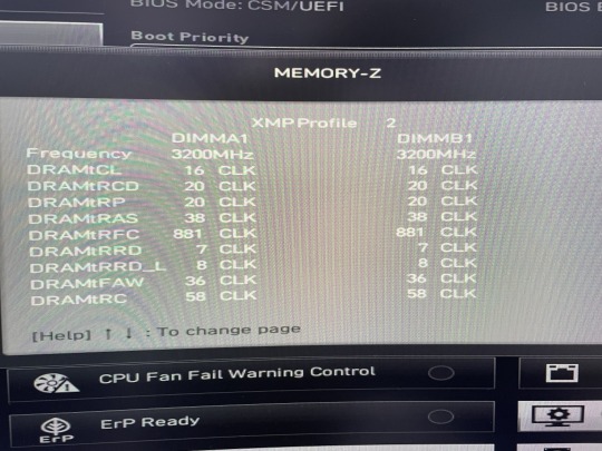
AMD 平台手動套用記憶體 XMP 設定
前陣子架設了 AMD 5600G 平台,當時配套的是DDR4 3600記憶體,但後來發現平台實際上只跑了DDR4 2666的速度。
經確認原來我用的這條記憶體的JEDEC標準時脈只到2666MHz,剩下的3200MHz和3600MHz是屬於Intel XMP設定。
雖然AMD平台可以透過各家主機板的快速超頻功能套用XMP設定,但我的MSI A520 主機板偏偏就只能套用3600MHz的設定,這已經超過AMD原廠支援的3200MHz了,若要符合,就必須手動處理:
1. 先確認記憶體的XMP設定內容。透過CPU-Z這套軟體可以查到XMP中包含時脈、電壓、主要CL延遲時間等對效能影響較大的參數,但若要看到細部的CL延遲時間,還是要藉由主機板BIOS提供的查詢功能。(底下是MSI的MEMORY-Z查詢畫面)
2. 套用最高的JEDEC標準時脈後,重啟電腦進入BIOS…
View On WordPress
0 notes
Text
The SK Hynix ZUFS 4.0 NAND Solution Improves On-Device AI
NAND Solution ZUFS 4.0
Zoned Universal Flash Storage (ZUFS) is a NAND Flash solution designed to increase data management effectiveness. By storing data with comparable properties in the same zone of the UFS, the product a flash memory product for various electronic devices like digital cameras and mobile phones optimizes data operating system-storage device transfer.
2On-Device AI: This is a technology that allows AI operations to be implemented directly on the device, bypassing the need for a physically separate server to do computation. The direct information gathering and processing capabilities of smartphones enable quick responses from AI systems and offer enhanced, personalised AI services.
According to SK Hynix, the ZUFS 4.0 is the greatest product of its kind on the market and is optimized for on-device AI from mobile devices like smartphones. The current device is expected to help the business extend its leadership in AI memory to the NAND arena, building on its success in the high-performance DRAM market, which is dominated by HBM.
Using unique technology, the ZUFS organizes and stores data from smartphones in several zones based on specific attributes. The newest product, in contrast to a traditional UFS, divides and stores data in distinct zones for comparable purposes and frequencies. This increases the performance of the operating system on smartphones and improves the efficiency of storage device management.
When compared to a traditional UFS, the ZUFS reduces the amount of time needed to execute an application from a smartphone during extended hours by 45%. The product’s lifespan increased by 40% as the problem of read and write performance deterioration was resolved more than four times over.
The technology was first developed in 2019, before to the commencement of the AI boom, when SK Hynix partnered with a multinational platform service provider in anticipation of a rise in the market for high-performance NAND solutions.
Following the delivery of the ZUFS prototypes, SK Hynix and the client worked together to build the 4.0 product, which satisfies JEDEC’s requirements. In the third quarter, SK Hynix plans to start mass producing the ZUFS 4.0 with the goal of supplying different on-device AI smartphones for international businesses.
Customers are demanding better memory options as large tech businesses concentrate on developing on-device products and implementing their own generative AI applications, according to Ahn Hyun, Head of the N-S Committee at “SK Hynix will create high-performance NAND solutions to meet these expanding needs to dominate global AI memory. time and forging closer relationships with top ICT companies.”
Leading memory chip maker SK Hynix has unveiled ZUFS 4.0 (Zoned Universal Flash Storage), a major advancement for smartphone technology. The purpose of this next-generation mobile NAND technology is to enhance smartphone on-device AI features.
Recognising the Need: AI’s Storage Requirements
Advances in storage solutions are required due to the growing world of on-device AI applications in smartphones, which include capabilities like voice assistants, intelligent cameras, and facial recognition. For best results, these AI features strongly rely on effective data storage and access. AI applications are need more and more data throughput, and traditional NAND storage is finding it difficult to stay up.
ZUFS 4.0: A Focused Method for Storage
ZUFS 4.0 uses a unique architecture to carefully arrange and store smartphone data in zones that are chosen based on certain criteria, thereby addressing these issues. Data with comparable usage patterns and retrieval rates are grouped together thanks to this clever allocation. There are several advantages to this focused storage strategy:
Improved Performance
ZUFS 4.0 dramatically lowers read and write latencies by allocating commonly utilized AI data to zones that are easily accessible. This means that your smartphone’s AI apps will run more quickly and seamlessly.
Enhanced Durability
As write cycles pass, traditional NAND storage experiences a decline in performance. By intelligently controlling write operations across many zones, ZUFS 4.0 lessens this problem. This keeps the storage device operating at a steady state for a longer period of time and increases its lifespan.
Optimised Power Efficiency
The storage unit uses less power because of the optimised data organisation within zones, which simplifies data access. This means that your smartphone’s battery life will be longer.
ZUFS 4.0: A Positive Sign for On-Device AI in the Future
ZUFS 4.0, an innovation from SK Hynix, is a big step towards smartphones having strong on-device AI capabilities in the future. This technology has the ability to completely transform a number of smartphone usage characteristics, improving the efficiency and smoothness of AI-powered features. ZUFS 4.0 is expected to be included into future smartphone models from top manufacturers, ushering in a new era of intelligent mobile experiences, with mass production scheduled for Q3 2024.
Beyond the Synopsis: Extra Interesting Information
Here are some more things to consider if you want to go deeper:
Technical specifications of ZUFS 4.0 architecture: How do data allocation and zone management work inside the storage device?
ZUFS 4.0 and conventional NAND systems are compared: Examine quantifiable data regarding increases in power efficiency, durability, and performance.
ZUFS 4.0’s effects on particular AI applications: What impact will this technology have on the advancement and functionality of AI capabilities on smartphones, such as facial recognition and natural language processing?
You can obtain a deeper comprehension of ZUFS 4.0 and its capacity to influence on-device AI in the smartphone industry by exploring these domains.
Read more on govindhtech.com
#AI#artificialintelligence#ZUFS 4.0#AIApplications#aiapp#AIDevelopment#smartphone#SKhynix#news#technews#technologynews#technologytrends#technology#govindhtech
0 notes
Text
Lenovo kondigt eerste laptop met Lpcamm2-geheugenmodules aan
Lenovo heeft de ThinkPad P1 Gen 7 van tenminste 2450 euro aangekondigd. De workstationlaptop is de eerste die met dunne Lpcamm2-geheugenmodules wordt uitgerust. Dit type geheugen wordt door Micron gemaakt en is gebaseerd op de CAMM2-standaard van Jedec. http://dlvr.it/T63nhd
0 notes
Text
JEDEC Extends DDR5 Memory Spec to 8800 MT/S, Adds Anti-Rowhammer Features
https://www.anandtech.com/show/21363/jedec-extends-ddr5-specification-to-8800-mts-adds-anti-rowhammer-features
0 notes
Photo

JEDEC amplía la especificación de memoria DDR5 a 8800 MT/s y agrega funciones anti-martillo de fila Cuando JEDEC lanzó su e... https://ujjina.com/jedec-amplia-la-especificacion-de-memoria-ddr5-a-8800-mt-s-y-agrega-funciones-anti-martillo-de-fila/?feed_id=600641&_unique_id=662665df461e5
0 notes
Text
JEDEC Extends DDR5 Memory Specification to 8800 MT/s, Adds Anti-Rowhammer Features
http://i.securitythinkingcap.com/T5rRjd
0 notes
Text
Lenovo, dünyanın ilk yeni nesil belleğe sahip dizüstü bilgisayarı P1 Gen 7'yi tanıttı

Lenovo'nun yeni ThinkPad P1 Gen 7 Workstation , resmi olarak dünyanın ilk LCAMM2 bellek modüllerine sahip ilk dizüstü bilgisayarıdır . LPCMM2, CAMM2'yi temel alan , DDR5 SO-DIMM'lerden daha küçük ve LPDDR5X bellek kullanımı sayesinde güç açısından daha verimli olan yeni bir bellek türüdür . Ayrıca geleneksel LPDDR5X çözümlerinin aksine dizüstü bilgisayarınızın belleğini yükseltmeyi de mümkün kılar.
ThinkPad P1, Lenovo'nun ThinkPad markalı profesyonel tüketici dizüstü bilgisayarlarının en son versiyonudur. Gen 7 modeli, P1 serisinde Micron'un LCAMM2 belleğini taşıyan ve maksimum desteklenen 64 GB kapasiteye sahip tek modeldir. Bu, daha yüksek kapasitelere ulaşabilen SO-DIMM seçeneklerinden biraz daha düşük olsa da, LPCMM2 ile Gen 7 sürümü, 7467 MT/s hızında çalışan LPDDR5X modüllerine erişimi olan tek ThinkPad dizüstü bilgisayardır. Resmi CAMM2 standardı 128 GB'a kadar veriyi işleyebilir, dolayısıyla Gen 7'nin maksimum bellek kapasitesi gelecekte değişebilir.
ThinkPad P1 Gen 7, Intel Core Ultra 9 185H Meteor Lake CPU tarafından desteklenen, 16:10 en boy oranlı OLED ekrana sahip 16 inçlik bir kasa kullanıyor. GPU olarak, Intel entegre grafikleri ve harici Nvidia GPU seçenekleri biçiminde geliyor; bunlardan sonuncusu, RTX 3000 dir.
Micron'un LCAMM2'si, dizüstü ve masaüstü bilgisayarlar için tamamen yeni CAMM2 JEDEC bellek standardını destekler. Daha önce de belirtildiği gibi yeni standart, geleneksel SO-DIMM belleğe kıyasla tamamen farklı bir form faktörü kullanıyor. Bu iki amaca hizmet eder. Birincisi, CAMM2 tabanlı bellek türlerinin önemli ölçüde daha az alan kullanmasını sağlamasıdır. İkincisi ise LPDDR5X çözümlerinden farklı olarak LPDDR5X modülünü daha yüksek kapasiteli bir seçenekle değiştirebilirsiniz.
LPCMM2, 7.500 MT/s hızında LPDDR5X belleği kullanarak standart JEDEC DDR5 SO-DIMM belleğinden 1,3 kat daha fazla bant genişliği sağlar. Tek bir modül, CPU bellek denetleyicisinin 128 bitlik bellek veri yolu genişliğinin tamamını kullanır; bu, tek bir LPCAM2'nin çift kanallı bir çözüm olarak işlev görmesi anlamına gelir.
Read the full article
0 notes
Text
What are the reliability standards for Discrete Semiconductor Products?
When it comes to the reliability of Discrete Semiconductor Products, several standards and factors play a crucial role. These standards are essential to ensure that the components meet certain quality and performance criteria, providing users with reliable and long-lasting products.
One of the key standards is the JEDEC (Joint Electron Device Engineering Council) standards. JEDEC standards cover a wide range of aspects, including environmental and mechanical testing, as well as electrical and thermal characteristics. These standards help manufacturers ensure that their products can withstand various environmental conditions and operate reliably over their intended lifespan.
Another important standard is the AEC-Q101 standard, which is specifically designed for automotive-grade discrete semiconductors. This standard sets rigorous requirements for reliability, ensuring that the components can withstand the harsh conditions often encountered in automotive applications.
Additionally, manufacturers often adhere to their own internal quality standards and testing procedures to further enhance the reliability of their products. These internal standards may include additional testing and quality control measures tailored to the specific needs of their products and customers.
Overall, adherence to these standards and rigorous testing procedures helps ensure that Discrete Semiconductor Products meet high reliability standards, providing users with dependable and long-lasting components for their applications.
0 notes
Link
In a breakthrough for computing technology, the JEDEC Solid State Technology Association has recently embraced a new form factor for laptop RAM, named CAMM2. This innovative technology stands out for its compact design and enhanced speed capabilities, dwarfing the traditional SO-DIMM standard. CAMM2, also known as LPCAMM2, is a game-changer for both designers and users, offering the first-ever modular LPDDR-based memory solution. LPCAMM2 combines the speed and efficiency of LPDDR5X components in a modular form. This advancement is significant as it allows for up to 16 DRAM components to be stacked within a single package. This not only simplifies memory architecture but also significantly reduces the space required within laptops, promising designs that are up to 64% more compact than those with dual-SO-DIMM stacks. This opens up possibilities for thinner, lighter laptops, potentially transforming the user experience. However, LPCAMM2 is not without its challenges. The requirement for a new type of socket could initially increase costs, despite the long-term savings anticipated from its design that fills both memory channels with a single module. Additionally, the tech industry is witnessing a trend where companies like Apple are integrating memory directly into processors. This approach, while eliminating traditional bottlenecks and enhancing efficiency, might pose a significant hurdle for the adoption of LPCAMM2. While LPCAMM2 represents a significant step forward in memory technology, offering benefits such as reduced energy consumption (a particular advantage for data center operators), its full adoption in the laptop market might take time. The tech industry's current direction towards integrating memory and processors suggests that LPCAMM2, despite its advantages, might not completely reverse this trend. In summary, LPCAMM2’s introduction is a major development in computer memory technology, heralding a future where laptops are thinner, lighter, and more efficient. However, its path to becoming a dominant technology in the field is not without obstacles, as the industry continues to evolve rapidly with different approaches to memory integration.
0 notes
Text
GDDR7-muisti on monella tapaa parempi kuin GDDR6 - Muropaketti.com
0 notes
Text
Z890 motherboards with Arrow Lake-S CPUs and Thunderbo

Intel Z890 Motherboard
Intel Z890 Motherboard Will Have Up To 4 “Arc Xe-LPG” iGPU Cores and Native Thunderbolt 4 Support for Arrow Lake Desktop Processors. Half of the iGPU “Xe-LPG” cores in Intel Arrow Lake-S desktop CPUs will be Meteor Lake, and Z890 motherboard will natively support Thunderbolt 4.
Information about the corresponding 800-series platform and Intel’s Arrow Lake-S “Core Ultra 200” Desktop CPUs is beginning to take shape. The highest Z890 chipset and iGPU configurations.
Z890 Motherboard release date
Intel Z890 motherboard are expected in 2[024] or early 2025. Next-generation motherboards will support Intel Arrow Lake CPUs.
Insights from leaks and rumours:
LGA 1851 is a new socket, thus LGA 1700 coolers won’t work.
DDR5 only Z890 doesn’t support DDR4.
PCIe: Gen 5.0 lanes provide bandwidth for faster graphics cards and storage devices.
Thunderbolt 4: Expected to be standard, allowing quicker data transfer and multiple high-resolution screens.
In general, Intel Z890 motherboard will be better than Z690 ones. They support the newest CPUs, memory, and storage, making them suitable for gamers and power users.
Z890 motherboard Rumors’ and leaks may change specs:
The Intel Core Ultra 200 “Arrow Lake-S” Desktop CPUs will commence with Core Ultra 5 SKUs and will be based on the first-generation Core Ultra 100 “Meteor Lake” family. In a prior study, found here, they have discussed the three potential “Unlocked” SKUs: Core Ultra 9 285K, Core Ultra 7 265K, and Core Ultra 5 245K.
It appears that the Core Ultra 3 chip will not be part of the portfolio, and Intel will probably continue to sell and update its current Core i3 CPUs in order to make up for the entry-level demand which, despite entry-level costs, is not as high as it appears. A refresh with entry-level SKUs on the current LGA 1700 platforms, like the forthcoming Bartlett Lake-S Desktop processors, may be provided by Intel.
Based on the Alchemist Xe-LPG graphics architecture, the Intel Arrow Lake-S “Core Ultra 200” Desktop CPUs can have up to 4 Xe-Cores in terms of iGPU configurations. Compared to the best Intel Core Ultra 9 “Meteor Lake” CPUs, these have half as many cores, and some SKUs should also have three and two Xe-cores. Since these also include four Xe-core iGPUs, you can use the Intel Core Ultra 7 165U/155U performance tests as a guide to see how these iGPUs perform.
Because desktop processors have larger TDPs, their clock speeds should be greater as well. Performance should be respectable, but don’t anticipate much. They would undoubtedly fall short of the best AMD Ryzen 8000G APUs, which that studied here currently provide competitive and occasionally even quicker performance than the top dies from Meteor Lake with 8 Xe-cores.
Regarding the cache, it appears that there is another leaker who has identified a maximum of 3 MB of L3 cache for each Lion Cove P-Core. According to MebiuW, the Skymont E-Core cluster, which consists of 4 E-Cores, will have a 3 MB L3 cache, whereas the Lion Cove P-Core will have a 3 MB L3 cache. As a result, the total cache for the top 24 core CPUs (Core Ultra 9 285K), the 20 core CPUs (Core Ultra 7 265K), and the 6+8 core configurations is now 36 MB, 33 MB, and 24 MB.
Last but not least, there is fresh information on the best Intel Z890 motherboard that will be included in the 800-series platform. According to reports, these motherboards have native support for Thunderbolt 4, along with a number of additional enhancements that should allow for quicker memory due to the upgraded Arrow Lake-S (Core Ultra 200) memory controller, among other things.
What is currently known regarding desktop CPUs from Arrow Lake-S is as follows:
LGA 1851 Socket Life Expected to End in 2026; DDR5 Only Compatibility; DDR4 Not Supported
Begins with motherboards from the 800-Series
Up to DDR5-6400 Memory Supported (Native JEDEC)
PCIe Gen 5.0 Lane Increases Via CPU & PCH
The first desktop family supported by Arrow Lake-S (DIY) CPUs have features P-Core L2 Cache of 3 MB
Features of Arrow Lake-S CPUs iGPUs Alchemists
Features of Arrow Lake-S CPUs CPU SKUs: 8+16, 6+8
Lake Arrow-S 8+16 (24 Cores)
Lake Arrow-S 6+8 (14 Cores)
Lack of Hyper-Threading Assistance
In the second half of 2024
Additionally, a tiny birdie has informed us that Intel 800-series motherboards will soon be in use.
Thunderbolt 4 compatibility on Z890 motherboards
New naming system: Arrow Lake-S CPUs will be called Core Ultra 200 series. This replaces Core i9, i7, and i5.
Additional cores: The flagship Core Ultra 9 285K may feature 24 cores (8 performance and 16 efficiency), and the Core Ultra 7 265K may have 20.
Updated socket that works with older coolers: Although Intel informs us that coolers compatible with LGA 1700 sockets will also work with LGA 1851, Arrow Lake-S CPUs will use the new LGA 1851 socket.
DDR5 only: The Arrow Lake-S will only work with DDR5 memory, in contrast to earlier generations that supported both DDR4 and DDR5 memory.
Additional capabilities include Alchemist integrated graphics, support for PCIe Gen 5.0, and Thunderbolt 4 compatibility on Z890 motherboard.
Z890 motherboard price
Since Z890 motherboards haven’t been formally released yet, it’s difficult to provide an exact price. But we can speculate a little bit based on the Z790 boards’ current price and reported features:
Price Range: Z890 motherboards could be anticipated to be in the range of the more expensive Z790 versions, if not more. Z890 boards can start at $250 and go up to well over $1000 for the highest-end variants with all the bells and whistles. Z790 boards range in price from $200 to $800.
Amounts Determining Price: Features like power delivery modules (VRMs), the quantity of PCIe slots, networking and WiFi capabilities on board, and the reputation of the brand will all affect the ultimate cost. The pricing will increase for high-end features like numerous Thunderbolt 4 ports and sophisticated overclocking capabilities.
Read more on govindhtech.com
#Z890#Motherboard#CPUs#intelarrowlakes#graphicscards#MeteorLake#IntelCoreUltra7#amdryzen#DDR5memory#news#technews#technology#technologynews#technologytrends#govindhtech
0 notes
Link
GDDR7 es el primer estándar que se centra tanto en la mejora del ancho de banda como en las necesidades de la industria RAS, dijo JEDEC, proporcionando una mejor solución de memoria para mercados en crecimiento como los juegos en la nube, las aplicaciones de inteligencia artificial y los centros de datos. Todos en la industria de los semiconductores están de acuerdo con el soporte GDDR7: AMD habla de un estándar de memoria innovador y Nvidia expresa su "entusiasmo" por la adopción de la señalización PAM como base de GDDR7.
0 notes
Text
JEDEC Publishes GDDR7 Graphics Memory Standard
https://www.jedec.org/news/pressreleases/jedec-publishes-gddr7-graphics-memory-standard
0 notes
Photo

JEDEC ya tiene listo el estándar LPDDR6, pero nos hará esperar Hasta el momento apen... https://ujjina.com/jedec-ya-tiene-listo-el-estandar-lpddr6-pero-nos-hara-esperar/?feed_id=556813&_unique_id=65f0524965baa
0 notes
Link
$159.00 $ TeamGroup T-Force Delta RGB 32GB DDR4 3200Mhz Desktop RAM Kit - Black https://nzdepot.co.nz/product/teamgroup-t-force-delta-rgb-32gb-ddr4-3200mhz-desktop-ram-kit-black/?feed_id=142580&_unique_id=65e4041cae924 Features: DELTA RGB DDR4 GAMING MEMORY – Full frame 120° ultra wide angle lighting – Built-in Force Flow RGB lighting effect – Aluminum alloy heat spreader with asymmetric minimalist design – Supports ASUS Aura Sync software synchronization – Latest JEDEC RC 2.0 PCB – Energy saving 1.2V~1.4V ultra low working voltage – Supports XMP2.0 one-click overclocking technology – QVL approved by all mainstream motherboard manufacturers Pursuing the perfect revolution The R on the heat spreader represents Revolution. The heat spreader is built with a lighter and thinner metal material. The hollow “R” design is very stereoscopic and matches with the […] #
0 notes
Last Seen Blogs

lucifersbby
👑👽💕💀

starhaze
✨🌛🌞🌜✨

thewidownatasha
TheWidowNatasha

lilpainy
𝑯𝒐𝒍𝒚 𝒑𝒓𝒊𝒏𝒄𝒆𝒔𝒔

witchwyfe
the boy is mine