#MultilayerPCB
Explore tagged Tumblr posts
Visit Tumblr Blog
Explore Tumblr blogs with no restrictions, modern design and the best experience.
Last Seen Tumblr Blogs


Fun Fact
Forty percent of Tumblr users are between the ages of 18 to 25.
Text

Looking for a high-precision custom PCB manufacturer?
At Hitech Circuits, we specialize in advanced multilayer PCB prototyping, tailored to your unique requirements.
Trace/space down to 3mil (0.075mm) Local fine-line spacing as tight as 2.5mil Impedance control within ±8% Hole tolerance up to ±0.05mm
Let us turn your complex PCB designs into reality. Get in touch today! hitechcircuits.com
0 notes
Text
#stackup#multilayerpcb#dfm#impedance#pcbmanufacturing#pcbmaterial#prepreg#core#pcbdesigner#pcbdesign#electronicsengineering#usa#europe
0 notes
Text
Designing Tomorrow: Aimtron’s Impactful PCB Assembly Solutions
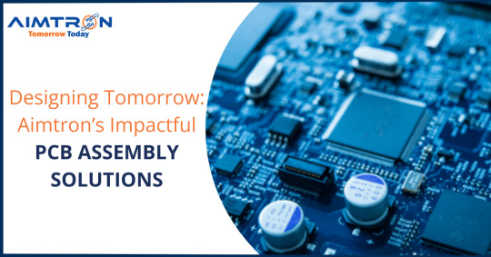
In the ever-evolving landscape of technology, Printed Circuit Boards (PCBs) play a pivotal role. These intricate electronic platforms serve as the backbone for countless devices, from smartphones to medical equipment. Among the trailblazers in this field is Aimtron, a company that doesn’t just design PCBs; it engineers solutions that shape the future.
Aimtron’s Vision and Expertise
Driven by a passion for progress and societal advancement, Aimtron excels in sourcing, building, and launching innovative products that enrich society globally. Their expertise in Electronic Design and Manufacturing Services sets them apart. Let’s delve into their impactful PCB assembly solutions:
1. PCB Assembly Services
At Aimtron, the journey from concept to production is seamless. Their dedicated team handles all your PCB needs, ensuring top-quality performance and reliability. Here are the types of PCBs Aimtron works with:
a. Flex PCBs (Flexible PCBs)
For applications requiring flexibility and durability, Aimtron’s flex PCBs are the ideal choice. Designed to bend and flex during use, these PCBs fit into tight or unusual spaces, providing reliable performance in dynamic environments.
b. Rigid-Flex PCBs
Combining the stability of rigid PCBs with the flexibility of flex circuits, Aimtron’s rigid-flex PCBs offer versatile solutions for complex electronic applications. These hybrid PCBs ensure reliability and performance, even in the most challenging environments.
c. Single-Sided PCBs
Ideal for simple electronic applications, Aimtron’s single-sided PCBs provide a cost-effective and reliable foundation for your components. They work well for low-density designs, ensuring quality and durability.
d. Double-Sided PCBs
With conductive layers on both sides, Aimtron’s double-sided PCBs offer more flexibility for complex circuits. These PCBs accommodate a higher component density, meeting the needs of sophisticated electronics.
e. Multilayer PCBs
For advanced electronic challenges, Aimtron’s multilayer PCBs provide the solution. Featuring three or more layers of conductive material, these PCBs are perfect for high-speed and high-frequency applications. They ensure signal integrity and reduce electromagnetic interference (EMI).
f. Rigid PCBs
Aimtron’s rigid PCBs offer a solid foundation for most electronics. Available in single-sided, double-sided, and multilayer configurations, they provide a stable and durable platform for a wide range of applications.
2. Chip-on-Board (COB) Technology
Aimtron employs COB technology, allowing direct attachment of bare semiconductor dies to the PCB. This results in smaller and more cost-effective solutions. The integration of COB technology enhances performance and reliability.
3. Design for Excellence (DfE)
Aimtron’s DfE method ensures efficient integration of components like PCBAs, wire harnesses, and mechanical enclosures. Collaborative engineering strategies streamline manufacturing, resulting in superior end products.
Conclusion
As we design tomorrow’s innovations, Aimtron’s impactful PCB assembly solutions pave the way. From flex PCBs to advanced multilayer designs, Aimtron’s commitment to excellence drives progress in the electronics industry. So, when you think of shaping the future, think Aimtron.
For more information, visit Aimtron’s website: Aimtron
#electronicsdesign#electronicsmanufacturer#pcbassembly#pcbassemblysolution#multilayerpcb#pcbdesign#pcbassemblyservices
0 notes
Text

Multi Layer PCBs 4 to 32 Layers
In-House manufacturing plant to manufacture Hi-end Multilayer PCBs
For more details visit : https://eiprismindia.in/
1 note
·
View note
Text
Laser Direct Imaging Equipment Market
The global Laser Direct Imaging (LDI) Equipment market was valued at 678.44 Million USD in 2021 and will grow with a CAGR of 2.4% from 2021 to 2027.
Get Free Research Report Sample PDF: https://cutt.ly/k0wxUTK
#imagingequipment#imagingequipmentmarket#laser#laserdirectimagingequipment#polygonmirror#dmd#hdipcb#icsubstrate#multilayerpcb#marektresearch#marketresearchreport#marketresearches#lifesciences#lifesciencesmarket#equipment#statsmarketresearch
0 notes
Photo

A multilayer PCB has multiple copper layers which are interconnected through copper plating vias, such as laser vias, NC vias, buried,blind vias, and plated through vias.
Such a circuit board has copper foil, adhesive, pre-peg, and core materials; all layered together under high pressure and temperature to make a multi-layer PCB. The pressure squeezes out the air, whereas the heat melts the adhesive to bind all layers.
A high-layer count PCB is a board with many layers,from 3 to 16, and more layers. In general, you will see an even number of layers in this reference like 4, 6, 8, 10, 12, 14, 16, 18, 20, etc. A multi-layer circuit board helps engineers create complex products.
A PCB with a high-layer count allows designers to implement high-speed and RF design techniques to have ground returns and a high-power distribution.
The BGA(ball grid arrays) of dense devices demand a multi-layer Printed Circuit Board to teach every possible signal.
Website: https://pnconline.com/ Facebook: https://www.facebook.com/PNCONLINE Twitter: https://twitter.com/PNCINC Instagram: https://www.instagram.com/pnc_pcb/ Tumblr: https://www.tumblr.com/blog/view/pncinc Myspace: https://myspace.com/pncinc2020 Bresdel: https://bresdel.com/pncinc Call us: (973) 284-1600 Email us: [email protected] Location: PNC INC, 115 East Centre St.Nutley, NJ, 07110
0 notes
Text
The difference between Double Layer PCB and Single Layer PCB
Before you start designing your PCB, you need to decide whether you will use a double-layer or a single-layer PCB. We widely use both of these in everyday electronic devices. The kind of PCB you use primarily depends on what you are using it for. If you intend to use your PCB in a complex device then you should go with double-layer and if you intend to use it in a relatively simpler device then you should go with a single-layer. The aim of this article is to explain the fundamental differences between the two and how to choose between them according to your requirements.
Double-Layer PCBs

You can also use a double layer board which commonly has two layers. These boards have one substrate layer like the single-layer boards. However, double-layer boards have two layers of conductive metal, one on each side. We can place the components on both sides as well.
Components on one side of double-layer PCB are connected to the components on the other side by using two different methods.
Single-Layer PCBs

Single-layer PCBs have a conductor material on one side and the components are placed on the other side. These boards have only one layer of conductive material which is mostly copper. A single-layer board has a conductive material, a substrate layer, a protective solder mask, and then the silkscreen. We mostly use these boards in simple electronic devices.
Through-Holes

In this method, we drill small holes through the board. Then we feed the wires, known as leads, through them. After that, we solder them to the correct component.
Surface Mounts

In this method, we solder the leads directly to the board. So, the board starts acting like the wiring surface for the components. Therefore, circuit implementation requires lesser space.
Comparison between the Single-Layer and the Double-Layer PCBs
Now we will compare these two types of PCBs by looking at their Pros and Cons.
Pros of Single-Layer PCBs
Lower Cost
Single-layer PCBs are much simpler than double-layer PCBs. Therefore, they require fewer resources to manufacture them. Hence, they are cheaper to produce.
Simpler Design and Production
Single-layer PCBs are simple to design and produce in comparison to the double-layer PCB. Therefore, we can design and manufacture them easily. So, we won’t need specialized equipment and skilled labor.
High Volume
Since we can easily design and manufacture these PCBs hence we can do their mass production without facing any issues. This will further decrease the manufacturing cost.
Short Lead Time
Single-layer boards have an easy manufacturing process. Therefore, they have a relatively small turnover time. So, they are the right pick when we immediately need PCBs in bulk quantities.
Pros of Double-layer PCBs
Increased Durability
Since these boards have more layers hence they are thicker. So, they are more durable in comparison to single-layer PCBs. This improved durability allows the PCBs to last longer and withstand rough conditions.
Useful for More Complicated Projects
Complex devices that involve more components often need a double-layer PCB. The double layers ensure that you have sufficient space for placing more components and connecting them. Hence, double-layer devices are ideal for advanced devices.
Smaller Size and Lighter Weight
Double-layer PCBs are lightweight and smaller in size. This is because layers are stacked over each other hence we can compress more components in a much tighter space. This smaller size leads to a reduction in weight.
Cons of Single-layer PCBs
Simplistic Design
The simplistic design of single-layer PCBs is their substantial limitation. A single-layer PCB won’t suffice when we need to make complex devices. The devices will not function properly if the wires cross each other. Hence, the board should have sufficient room for accommodating everything.
Slower Speed and Low Capacity
The speed and power of these boards are also affected by their limited number of connections. They have a low operating capacity and therefore they don’t have enough power for certain applications.
Larger Size
If you want to improve the capacity of a single-layer PCB then you will have to increase its dimensions. If you increase the size of the board then the finished product will have an increased overall weight.
Cons of Double-layer PCBs
Higher Costs
It is more expensive to use double-layer boards and it requires more resources. On top of that, we need skilled labor and sophisticated equipment.
Complicated Designing and Manufacturing
It is more complicated to design and manufacture double-layer boards. So, if you lack the resources then you might face many problems throughout the manufacturing process.
Longer Lead Times
Since double-layer boards are more complicated therefore they have a longer turnover time. If you make a mistake during the manufacturing process or if there is a flaw in the design then it will be very difficult to rework. Also, it will increase the overall cost.
Complex Repairs
Double-layer PCBs are very reliable, however, if they get damaged then it is very difficult to repair them. This is because of their complex design. A large number of components and their connections make it very difficult to identify and fix the problem.
Deciding Between Single-Layer or Double-Layer PCBs
If you want to determine whether you should go with single-layer or double-layer PCBs, then you should consider your requirements and which type of PCB is more suited for them. You may do so by asking yourself these five questions.
What level of functionality would I need?
You should go with double-layer PCBs if you need them for complex applications.
2. What is the maximum size the board can be?
Double-layer boards have a smaller size and they have improved performance.
3. Is durability a major priority?
You should go with double-layer PCBs if the answer is Yes.
4. What is my budget?
If you have a modes budget then single-layer PCBs are the best choice.
5. How quickly do I need the PCBs?
Single-layer PCBs have a shorter turnover time in comparison to double-layer PCBs.
MOKO Technology is a renowned name in the PCB industry. We have large manufacturing set up and we have mass production capacity. MOKO Technology specializes in manufacturing both the single-layer and double-layer PCBs. Feel free to reach out to us if you want a quote or if you have any questions.
0 notes
Photo

As soon as LED aluminum substrates came to the market, the development of the heat dissipation application industry started. Click here to know more about #LED #Aluminum #Substrates #multilayerpcb , #LightingProducts, #ElectronicRegulator, #Thermalresistance #assembly #electricity #leds https://lnkd.in/dYTkqKw
0 notes
Link
0 notes
Text
What is HDI PCB?
Do you remember IBM Simon? You can consider it the father of smartphones. The Simon phone has 38 mm thickness and almost 510g weight. So it was impossible to place in the pocket. On the other hand, look at today’s smartphone. You can easily put them in your pocket. And the reduction in the size of a smartphone is due to the HDI PCB. The purpose of HDI technology is to make devices smaller, thinner, and lighter as well.
So do you want to learn HDI PCB? This article gives you a clear idea about what is HDI circuit boards. So we will cover its features, benefits, and applications, etc. After completing this article, you will be adept in the HDI PCBs.
What is HDI PCB
HDI PCB stands for High-Density Interconnector Printed Circuit Board. It is one of the significant enhancement in the world of PCB electronics. Moreover, its advanced multiple via processes minimizes the number of layers. So it provides smaller yet most powerful circuitry.
Features of HDI PCB
HDI PCB fabrication uses the latest multilayer technology that allows you to integrate multiple layers with high density. This technology has significant dominance over other traditional PCBs. Here are some key features of this technology:
High-density interconnector uses laser drilling technology. So this technology precludes different drawbacks that occurred during traditional mechanical drilling technology. Therefore, it reduces your difficulties.
These boards contain high wiring density per unit surface area as compared to regular PCBs.
HDI boards most often come with apertures having a range of 3.0 to 6.0 mil. Moreover, the line width is between 3.0 and 4.0 mil. So by using these features, you can minimize the pad size significantly.
Another most popular feature of these boards is vias. There are different types of vias such as buried, blind and micro vias. The size of the vias can be lesser than 0.0006 mm in diameter. So these small size vias help you to save more space on the boards. So you can create a more compact design.
The effectiveness of these boards assists as a substitute to use of high-layer laminated boards. Moreover, these boards are expensive as well.
Different characteristics such as lightweight and high frequency. Plus, high electrical speed makes it the ideal option for various applications.
Different stack-ups for HDI PCBs
According to the IPC-2315 standard from the IPC, there are 6 basic types of stack-ups. These stack-ups types include I, II, III, IV, V and VI. However, the last three types are more expensive and have minimum use. So we will only discuss the first three types of vias. Moreover, the standard differentiates HDI stack-ups on the basis of the vias type. Such as micro, buried, blind and plated through vias.
HDI Type I: These types have a structure of a laminated core having at least just a single layer of micro vias. These vias can exist on one or both sides of the circuit. Type I HDI use blind and PTH vias. However, it doesn’t use buried vias.
HDI Type II: This type includes different blind and buried vias on a laminated core. Fabricators can stagger different micro vias and stack them relative to buried vias.
HDI Type III: To construct this type, the manufacturer uses micro vias, buried and blind vias on a laminated core. Moreover, this type includes at least two layers of micro vias on one side of the board or both. You can stagger micro vias over other micro vias. Furthermore, you can stack them over other buried vias.
Materials of HDI PCB Fabrication
Do you want to know about the different materials used in HDI PCB manufacturing? You should know about the different materials for various reasons. For example, if you know about the material, you can choose the right material for your HDI board. Let’s have a look at the most important material used for HDI:
Copper: This is the primary material for all PCBs.
Core: It is a skeleton of the board. It is a copper-clad board. You can use it for the double-panel production of the inner layer.
Surface treatment materials: It includes nickel-gold alloy, lead-tin alloy, OSP, silver, etc.
RCC: The specification of RCC includes 60T12, 60T18, 65T12, etc.
FR4 (LDP): The specifications of FR4 include 1080 and 106.
If you want your PCB to perform well, you will have to choose adequate dielectric and resin material. The properties of these materials include decomposition temperature and glass transition. It further includes thermal expansion coefficient and delamination time.
For example, most of the people go with FR4 materials. You can use it for those applications that need a few GHz frequencies. In addition to this, if you want to pick materials used in microwave/ RF applications. You need materials that are capable to maintain impressive signal integrity. So choose a material that can is good for up to 20 GHz.
And other material includes BT epoxy, polyamide, and enhanced epoxy. You can pick any of them according to your needs!
Benefits of using HDI PCB Board
Using HDI circuit boards in your application has a lot of advantages. Due to these benefits, most manufacturers prefer HDI over other types of circuit boards. Have a look at the benefits of using HDI PCB in your applications:
1. Reduce heat transferring
Traditional PCBs burn due to a lack of heat transferring. So this technology has an edge over traditional circuitry such that it reduces heat transfer. Why? It is because the heat has to travel for a short distance before leaving the HDI PCB.
The design of this circuity makes it capable to go through a high thermal expansion. So it increases the lifespan of the circuit boards.
2. Manage thermal conductivity
The availability of different types of vias makes sure the current transmission between the components. So it is up to you to fill these vias with either conductive or non-conductive materials. You can further enhance the functionalities by using the blind vias and via in pad components together.
Furthermore, the HDI boards have a compact structure. So it reduces the transmission distance between different components. It further reduces transmission times and crossing delays as well. So as a result, you will have a strong signal for your circuit.
3. Minimal power usage
HDI PCBs consume less battery power as compared to traditional ones. This is because of advanced manufacturing technology. This technology binds the electrical components resulting in minimizes loss of energy.
HDI circuits use vias instead of through holes that also reduce power usage. This effect increases the lifespan of your battery.
4. Smaller form factors
It is an ideal choice for saving space. You can easily minimize the total number of layers on HDI PCB desingning. For example, you can replace the 8-layer through holes by using a 4-layer via in pad solution. As a result, you will have a small PCB. Some vias will not visible to the people and increase performance as well.
5. Incorporation of components
You can’t only minimize the space but also incorporate your boards as well. It means you can put as many details as you want on the HDI board. Furthermore, you can populate both sides of the board to incorporate the components. So this depends on the design and the need for the application.
6. Different designs
By using the high-density interconnector technology, you can create different designs of the boards. So you can use these circuit boards in all applications as you want. Such as you can have rigid, flexible and combination of both.
How does HDI PCB change your lives?
HDI PCB is the fastest-growing part of different industries. Nowadays, devices are getting smarter and more portable. Furthermore, components insides the devices are smaller and lightweight. On the other hand, performance is getting higher and higher. In addition to this, performance works in smaller areas as well.
So all this happening just because of HDI circuits and other technologies similar to this. These circuits provide higher density per unit as compared to traditional circuit boards. This technology use buried, blind, and micro vias to uplift the performance. Besides, these vias provide high-quality results when combined with laser direct imaging and laser drilling machines.
Application of HDI PCBs
So far you have learned a lot of things about this amazing technology. However, you might be thinking that where you can apply these incredible circuit boards. So it is a fact that there are countless applications where you can use this board. Therefore, you can use this circuitry from simple to mega-complex applications. Here are some significant applications for HDI PCBs:
1. Consumer electronics
This term refers to all basic devices you find in your daily life usage. Such as laptops, smartphones, and cameras. Moreover, it also includes the majority of home appliances and entertainment systems.
All these gadgets need circuit boards having lighter weight. Moreover, these appliances also need flexibility. Thus, HDI circuitry meets the qualities of these gadgets.
2. Medical equipment
There are numerous electronics playing a key role in the wellbeing of our health. So the medical industry wants to ensure the high-quality circuits that meet their standards. So all medical equipment should be effective and play a major role in the safety of the patient.
So there are several devices where you will find HDI printed circuit boards. Such as monitors and scanners. It further includes heart pacemakers, scientific instruments and control systems.
3. Industrial applications
You can find this circuitry in the high-powered industrial applications. Due to its effectiveness and robust nature. Moreover, it consumes less energy and ensures maximum output.
Even these circuit boards are capable to perform in a harsh environment. So most boards use thick copper that helps in faster battery charging. Moreover, it also helps in high current applications as well.
So you can find this circuitry in various applications. Such as electric drills and different measuring equipment. Besides this, they exist in power equipment such as generators and solar power panels.
4. Automotive
Most automotive rely on different electronic parts to work properly. So you can use this technology in these applications. You can use high-frequency signals of RF and HDI PCBs combined with sensor applications. This is common in automotive.
Different technologies such as radar technology are clearing their way in the automobile industry. All such technologies rely on HDI circuitry.
In addition to this, some common applications such as engine management systems use this technology. It further includes navigation devices, video, and audio devices.
5. Aerospace applications
The precision and durability make HDI an ideal choice for aerospace applications. Moreover, HDI circuits can resist vibration effects. Airplane and jets need circuity that can withstand in harsh environments.
So HDI circuit boards ensure the security of aerospace applications. These apps include monitoring equipment such as pressure sensors. Plus, accelerometer.
Conclusion
The high-density interconnector circuit board is the most robust technology. You can use this technology in a wide number of applications. If you want to order high-quality PCB, you must be familiar with the basics of this technology.
So if you are looking for a reliable PCB, you can consult MOKO Technology. We utilize the latest technologies to create high-quality circuit boards.
0 notes
Text
Multilayer PCB boards are better than their alternatives
A multilayer PCB board is made from three or more conductive copper foils. These are glued and laminated together with layers of insulation between them. We use VIAS to achieve electrical connections between the layers. This allows us to make complex PCBs of various sizes.
The electronic products are becoming sophisticated with time and we need advanced PCBs. Conventional PCBs had problems like crosstalk, noise, and stray capacitance. So, we had to follow some design constraints. However, these design constraints didn't allow for the satisfactory performance of single-layer PCBs. Therefore, manufacturers came up with a multilayer PCB board.
Multilayer PCB boards are gaining popularity in modern electronics. They are available in different sizes so we can use them for numerous applications. Multilayer PCB boards can have 3-50 layers. However, layers are mostly used in even numbers because an odd number of layers can lead to circuit warping. Common applications need no more than 12 layers of these PCBs however some special applications can involve up to 100 layers. However, this is very rare because it reduces their cost-effectiveness.
Multilayer PCB boards are better than their alternatives
When we compare multilayer PCB boards to the single layer or double layer PCBs, then the benefits of multilayer PCB boards seem more prominent. Here, we will take a look at some of them.
1.Higher Assembly Density
Single layer PCBs have limited density because of their surface area. However, we can multiply the density of multilayer PCB boards through layering. Therefore, we can increase their functionality, speed, and capacity and reduce their size.
2.Smaller Size
Multilayer PCB boards have a smaller size in comparison to the single layer PCBs. We can increase the surface area of single layer PCBs only by increasing their size. However, we can increase the surface area of multilayer PCB boards by adding more layers. So, we can decrease their overall size. This allows us to use multilayer PCB boards even in very small electronic devices.
3.Lighter Weight
We can seamlessly integrate a large number of components in multilayer PCB boards. So, we need a smaller number of connectors. Therefore, multilayer PCB boards are lightweight and are ideal for complex electronic applications. Multilayer PCB boards have the same functionality as that of a single-layer PCB. However, they require fewer connections and have reduced weight. This is empirical for smaller devices where we are concerned with the overall weight.
4.Functionality Enhancement
Multilayer PCB boards are more capable than the single layer PCBs. They have controlled impedance, greater design quality, and improved EMI shielding. So, we can accomplish more with them as compared to single layer PCBs.
Multilayer PCB boards still exist some limitation
Despite their advantages, multilayer PCB boards have some limitations. Therefore, we should also take a look at them.
1.Higher Cost
Multilayer PCB boards manufacturing is more expensive as compared to double layer and single layer PCBs. Multilayer PCB board design is difficult so we need more time to work out any possible problems. They have a complex manufacturing process so there are high labor costs. Additionally, the equipment we use for multilayer PCB boards fabrication is a little expensive.
2.Complicated Production
Multilayer PCB boards are difficult to manufacture and they require sophisticated manufacturing techniques. So, a multilayer PCB board can become useless even if there is a small flaw in the designing or manufacturing process.
3.Need for Highly Skilled Individuals
Multilayer PCB boards require extensive designing before we can manufacture them. If we lack experience then it can be very difficult. Interconnection is required between different layers of a multilayer board. However, we have to avoid impedance issues and crosstalk. Therefore, we need to be careful because a single flaw in the design can lead to a non-functioning PCB.
4.Production Time
There are more manufacturing steps involved as the complexity increases. This affects the turnover rate of multilayer PCB boards. Every multilayer PCB board needs a considerable amount of time to manufacture. This leads to longer wait times between when an order is placed and when you deliver the product.
Tips for Designing Multilayer PCB boards
Designing an efficient multilayer PCB board requires a lot of focus and care. So, here are some tips which can help you with the designing process.
1.Board size
If you set your board size first then it will give you a constraint for determining other elements of your multilayer PCB boards. The optimal board size depends on the size and number of components. It also depends on the location where you will mount your board, tolerance for spacing, drill holes, and clearances.
2.Layer design
You can use PIN density for finding the number of layers you will need for your board. For layer design, you should consider impedance requirements, especially if you are using controlled or fixed impedances.
3.VIAS selection
The VIAS you choose for your board will affect the complexity of manufacturing. So, this will affect the quality of your multilayer PCB boards.
4.Material selection
You should select the material for manufacturing your board by using a layer by layer approach. However, you must ensure that the material allows for good signal integrity and ground plane distribution.
5.Optimize the manufacturing process
Your design decisions will affect the performance of your multilayer PCB board. You should carefully choose clearances, solder masking, drill hole sizes, and trace parameters. All of these significantly influence the manufacturing process.
Thickness Standard for Multilayer PCB board
The typical thickness of PCBs was 1.57 mm or 0.063 inches in the past. This was standardized because of the substrates of plywood sheets. However, when we started developing multilayer PCB boards then we had to follow the thickness of connectors between layers. So, the required thickness became variable. However, a general standard is thickness from 0.008 to 0.240 inches. You can choose the PCB thickness depending on your needs and applications.
MOKO Technology is a renowned name when it comes to manufacturing PCBs. We specialize in all kinds of PCBs including multilayer ones. We have the capability for mass production and we can incorporate any number of layers in our boards. If you are looking for a reliable supplier for custom made multilayer PCB boards service, then you are in the right place! Feel free to contact us if you want a quote or have any queries.
0 notes
Text
What is multilayer PCB?
Complete Guide about Multilayer PCB
Multilayer PCB is a type of circuit board that contains three or more layers of conductive material. These boards increase the available area for wiring. Whenever we talk about a number of layers, it means we are considering a number of conducting patterns on the board. Multilayer PCBs are normally Rigid PCB. It is because it is very difficult to create it in a flexible format.
The number of layers depends on your needs. So layers could be up to 100. However, 4 to 8 layer PCBs have common usage in various applications. Circuitry gets complex when layers increase. So you can customize different numbers of layers according to your needs.
Different essential components of multilayer PCB
There are 4 main components of multilayer PCB as follows:
Substrate: it is the most important part usually made of fiberglass. Fiberglass provides the core strength to the PCB and resists against breakage. You can consider the substrate as a skeleton of PCB.
Copper layer: It depends on the board type. So this layer can be either full-on copper or a copper foil. Regardless of the board type, the copper layer is still the same. So copper carries electrical signals to and from the PCBs. You can consider this layer as a nervous system. That carries signals from the brain to your muscles and vice versa.
Solder Mask: It is a layer of polymer that protects the copper layer. So it basically prevents short-circuit when copper comes into contact with the environment. So you can consider the solder mask as the skin of the PCB.
Silkscreen: It is the final part of the PCB. The silkscreen basically shows part number, symbols, and logos of different components on the board. Furthermore, it also provides information like symbols switch settings, test points, and component references.
How to manufacture Multilayer PCB?
Here is the complete step by step guide for manufacturing multilayer PCB:
1.Designing
The first and foremost step to design PCB and prepare them for production. All manufacturers have their own approach to this process. Generally, the designer lays out a blueprint for the circuitry and fulfills all the outlined requirements. Different types of software are available for designing such as Extended Gerber.
So you can use Extended Gerber or any other tool to design your circuit. Once you design the circuit, carefully check the entire design. Make sure that there is no error in the entire blueprint. After designing, you can send this blueprint to the fabrication house to start building circuitry.
2.Photo Plotting
In this step, you can use a laser photo-plotter to plot a film for each individual layer. A laser photo-plotter is a tool used to create photo-tools for solder mask and silkscreen. The thickness of the film is about 7 mils.
Many manufacturers use special laser direct imaging equipment that images straightly onto the Dry Film. This technique reduces costs. Furthermore, the process is more accurate and effective. So you can produce internal as well as external layers using laser direct imaging (LSI).
3.Imaging and Develop or Etch
This process applies the primary images such as pads and traces onto the circuit board. Besides this, the DES process creates the copper pattern for the plating. Here is what to do in this step:
Apply photo imageable to the copper panels.
Furthermore, image the panels using LSI.
Etch off the whole exposed copper from the panel.
Strip the remaining Dry Film and just leave the remaining copper pattern for the inner layers.
4.Automated Optical Inspection
AOI basically inspects different layers of multilayer PCB before laminating all layers together. The optics compare the PCB design data to the actual image on the panel. Any differences such as missing or extra copper can result in opens or shorts. So this process basically helps manufacturers to catch any defect in the circuitry.
5.Oxide
Oxide is a chemical treatment to inner layers before lamination for multi-layer PCBs. Moreover, the oxide code is brown or black depends on the process. It is an important step to increase the roughness of copper to enhance the laminate bond strength. Furthermore, this process prevents the separation between different layers of the base material.
6.Lamination
To produce a multilayer PCB, different layers of epoxy-infused fiberglass are laminated together. For lamination, manufacturers apply high temperature and pressure using a hydraulic press. The presser and heat cause the fiberglass sheet to melt and tightly join the layers together. After cooling this material, it further follows the same manufacturing process as a double-sided PCB.
7.Drilling
All PCBs need some holes to link copper layers, attaching components and mounting the PCB. So you can drill holes using some advanced drilling systems. These systems use solid carbide cutting tools. Furthermore, these have a design for the fast removal of chips in abrasive materials.
A pre-programmed drill machine drills specific-sized holes at the exact location. So the drill machine works according to the designer’s provided data. Designers provide this information as a numerically controlled drill file.
In addition to this, a thin sheet of aluminum acts entry material. Besides this, hard cardboard acts as exit material. So this technique keeps the drilling smooth and avoids creating different fibers.
8.Electroless Copper Deposition
After drilling, manufacturers deposit a thin coat of copper on the exposed surfaces of the panels chemically. Furthermore, they deposit a copper coat on the hole walls using electroless plating.
9.Dry Film Outer Layer
After copper deposition, you must apply the outer layer images to prepare the panel for electroplate. So you can utilize a laminator machine to coat outer layers with the dry film. The dry film is a photo imageable material. Moreover, this process is almost similar to image the inner layers of a multilayer PCB.
10.Plate
The electroplating process involves copper plating onto the conductive pattern. Plus on the hole walls of the PCB as well. The thickness of the plating is around 1 mil. After copper plating, you need to deposit a thin layer of tin plating. The tin plating layer serves as an etch barrier.
11.Striping and Etching
After completing the plating process on the panel, the dry film remains. But you need to remove the copper that lies beneath. Now the panel will go through the SES process. So SES stands for String Etch Strip.
In this process, you need to etch the exposed copper. It means you will remove the uncovered area of copper by tin. So traces and the pads around the holes and copper patterns remain there. At last, you will remove the remaining tin that is covering holes and traces chemically. So after completing this step, you only leave behind exposed laminate and copper of the PCB.
At this stage, the skeleton of the PCB is complete now. Now all onwards steps are related to protecting PCB.
12.Solder Mask and Legend
Most manufacturers use a liquid photo imageable (LPI) Solder mask to protect the copper surface. It further protects solder bridging between different components during assembly.
LPI solder mask is basically a photo-sensitive epoxy-based resist. You can cover the entire panel by using the screen printing process. There are some other alternative methods to the traditional screen plating. So you can use such an alternative for solder masking.
After the solder mask, you can apply legend. It prints different symbols and letters on the PCB for reference during assembly.
13.Surface Finish
It is the last and final chemical process to manufacture a multilayer printed circuit board. Solder mask covers almost all circuitry. So the surface finish prevents oxidation of the remaining exposed copper area.
This is an important step because you cannot solder the oxidized-coper. Furthermore, you can use different types of surface finish for this step. Such as you can you hot air solder level (HASL).
The benefit of multilayer PCB
Here are some advantages of multilayer PCB over other types:
It has a higher assembly density than single and double-layer PCBs.
There is no need for cables to interconnect different components. So it is an ideal choice for low weight PCBs.
These PCBs come in smaller sizes resulting in reduced space requirements.
EMI shielding is straightforward and flexible.
Flexibility is another factor that stands out multilayer PCB among all printed circuit boards.
Different applications of multilayer PCB
Many electronic components use a multilayer PCB. Moreover, these circuits encompass intermediate to complex range of circuitry structure. Here are some significant applications of multilayer PCB:
Heart Monitors
Cell phone transmission and repeaters
Atomic accelerators
Space probe and X-ray equipment
Weather analysis and GPS technology
Data storage and file servers
Fiber optic receptors and Cat scan technology
How to identify a multilayer PCB
If you have some PCBs and want to check the total number of layers, you can follow these steps.
Expose the edge of the circuit board to the light to see the copper planes. So in this way, you can easily watch trances more closely. Even if the multilayer PCBs don’t contain blind via, you can still utilize bright light to analyze the inner layers.
The best place to detect the inner layers is where no path and lines visible on the outer layers. Moreover, the majority of manufacturers print the label to identify the total number of a layer on the circuit board. So by just looking at the edges, you can identify the total number of layers.
0 notes