#PCB Chip Surface Mount LED
Explore tagged Tumblr posts
Visit Tumblr Blog
Explore Tumblr blogs with no restrictions, modern design and the best experience.
Last Seen Tumblr Blogs


Fun Fact
Tumblr has 411 employees.
Text
https://www.futureelectronics.com/p/semiconductors--optoelectronics--leds/sml-lx0603gw-tr-lumex-7962061
Optoelectronic devices, Isolation components, led display screen, led emitter
Green 0603 1.6 x 0.8 mm 160° Diffused 18 mcd 2.2 V PCB Chip Surface Mount LED
#Lumex#SML-LX0603GW-TR#Optoelectronics#LEDs#light control#optoelectronic applications#light emitting diode#Isolation components#led display screen#led emitter#Power Optoelectronics#PCB Chip Surface Mount LED#led monitor
1 note
·
View note
Text
Sharing a Computer with More Friends
A few months ago I built an I/O expansion board for my homebrew 68030 project with a 4-port serial card to go with it, and got BASIC running for four simultaneous users. It worked, but not as well as I had hoped. I wanted to be able to run two of those serial cards to support 8 total users, but it had proven unstable enough that with just the one card I had to slow down the whole system to 8MHz.
So I designed a new serial card.

I had previously been running this computer without any issues at 32MHz with a mezzanine card with FPU & IDE as well as a video card. The main board by itself can clear 56MHz. Having to go all the way down to 8MHz just didn't sit well with me. I want this machine to run as fast as possible for its 8 users.
I put extra time into reviewing worst-case timing for all components and graphing out how signals would propagate. The 16C554 quad UARTs I'm designing around are modern parts that can handle pretty fast bus speeds themselves — easily up to 50MHz with no wait states on the 68030 bus — assuming all the glue logic can get out of the way fast enough.
Signal propagation delays add up quickly.
My first draft schematic used discrete 74-series logic for chip selection, signal decoding, timing, etc. At slower bus speeds this wouldn't have been a problem. But I want this thing to run as fast as possible. By the time critical signals had made it through all those logic gates, I was looking at already being well into one wait state by the time the UART would see a 50MHz bus cycle begin.
I needed something faster. I was also running low on space on the board for all the components I needed. The obvious answer was programmable logic. I settled on the ATF22V10 as a good compromise of speed, size, availability, and programmability. It's available in DIP with gate delays down to 7ns. Where discrete gates were necessary, I selected the fastest parts I could. The final design I came up with showed a worst case timing that would only need one wait state at 50MHz and none for anything slower.
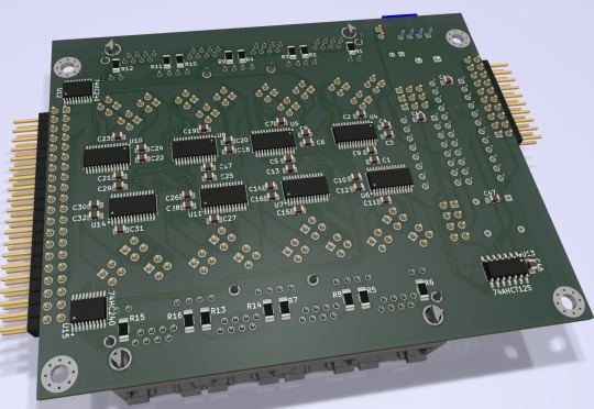
It ended up being a tight fit, but I was able to make it work on a 4-layer board within the same footprint of my main board, putting some components on the back side. (It may look like a bunch of empty space, but there's actually a lot going on running full RS232 with handshaking for 8 ports).
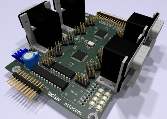
New problem. I had blown my budget for the project. As much as I love those stacked DE9 connectors, they're expensive. And there's no getting around the $10 pricetag for each of those quad UARTs. Even using parts on-hand where possible, I was looking at a hefty Mouser order.
[jbevren] suggested using ganged RJ45 connectors with the Cisco pinout instead of stacked DE9, to save space & cut costs. [Chartreuse] suggested buffering the TTL serial TX/RX signals to drive the LEDs that are frequently included on PCB-mount RJ45 connectors. Both great ideas. I was able to cut 20% off my parts order and add some nice diagnostic lights to the design.
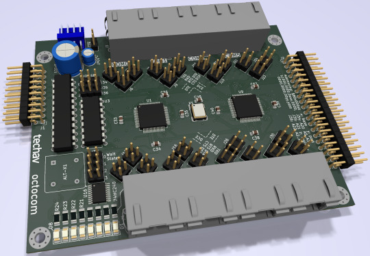
Two weeks later, I received five new PCBs straight from China. I of course wasted no time setting into starting to assemble one.
I really set myself up for a challenge on this one. I learned to solder some 25 years ago and have done countless projects in that time. But I think this might be the most compact, most heavily populated, most surface mount board I've ever assembled myself. (There are 56 size 0805 (that's 2x1.2mm) capacitors alone!)


After a few hours soldering, I had enough assembled to test the first serial port. If the first port worked then the other three on that chip should work too, and there's a great chance the other chip would work as well.

And it did work! After some poking around with the oscilloscope to make sure nothing was amiss, I started up the computer and it ran just fine at 8MHz.
And at 16MHz.
And at 25MHz.
And at 32MHz.
And at 40MHz.
And almost at 50MHz!
Remember what I said about my timing graphs showing one wait state for 50MHz? The computer actually booted up and ran just fine at 50MHz. The problem was when I tried typing in a BASIC program certain letters were getting switched around, and try as I might, BASIC just refused to 'RQN' my program. It was pretty consistently losing bit 3, likely from that signal having to travel just a tiny bit farther than the others. A problem that will probably be resolved with an extra wait state.
Good enough for a first test! A few hours more and I finished assembling the card.

I did have some problems with cleaning up flux off the board, and I had to touch up a few weak solder joints, but so far everything seems to be working. I've updated my little multi-user kernel to run all 8 users from this new card and it's running stable at 40MHz.
I need to update my logic on the 22V10 to fix a bug in the wait state generator. I would love to see this thing actually running at 50MHz — a 25% overclock for the 40MHz CPU I am currently running. I also want to expand my little kernel program to add some new features like the ability to configure the console serial ports and maybe even load programs from disk.
I hope to bring this machine with a collection of terminals and modems this June to VCF Southwest 2025 for an interactive exhibit that can be dialed into from other exhibits at the show.
#wrap030#multi-user BASIC#EhBASIC#homebrew computer#motorola 68030#68030#mc68030#motorola 68k#vcfsw#vcfsw2025#Retrocomputing#rtc#retrotech crew
31 notes
·
View notes
Text
LED PCB Assembly
What is the LED Circuit Board assembly?
Generally, LED PCB assembly is considered to be a circuit board that has the LED components soldered to it. The LED is soldered to the printed circuit board and features a chip that creates the light as electrically connected. A thermal heat sink and a ceramic base are used to bond the chip. Not all the PCB products can be used in Led industry, as an LED PCB is easy to create a high volume of heat, but making it hard to cool with traditional methods. For this reason, metal core PCB is widely used in LED application because of their enhanced ability to dissipate heat, especially aluminum pcb is often used to fabricate PCB for LED lights.
We’ve had great LED PCB assembly experiences with top LED chips to brand such as Cree, Luxeon, Osram, Nichia, Lumileds, MLS, EVERLIGHT, Samsung, LG, Seoul., etc. PCB LED lights can be incorporated into numerous lighting applications due to their combination of excellent energy efficiency, low cost and maximum design flexibility.

Application of LED PCB Assembly
Hitechpcba serves customers in different industries, providing highly reliable and innovative LED PCBs for various applications:
• Horticulture light LED PCB Assembly
• LED controller PCB Assembly
• Computer LED display and indicators
• LED lights PCB Assembly for medical use
• Automotive LED PCBs Assembly include PCBs for brake lights and headlights
• Street lighting LED PCB Assembly
• Flashlights and camping accessories
• Traffic light PCB Assembly
• Commercial lighting LED PCB Assembly
LED PCB Assembly specification
Number of layers for LED PCB
These layers are made up of aluminum and magnesium, but now have Copper base material and Ceramic base materials for LED PCB industry, we can meet it.
Aluminum LED PCBs stand out among other PCBs because it has a good insulation characteristic and has a better machinery performance, the cheap cost is one important factor too.
Types of layers for LED PCB Assembly
Normally, the base layer is made using aluminum alloy metal.
This aluminum alloy substrate used in making the base makes it ideal for through-hole technology which transfers and dissipates heat.
A thermal insulation layer is made using some ceramic polymer which has good viscoelasticity characteristics.
It is highly heat resistant and protects the PCB against heat and mechanical stress.
The circuit layer, which is covered by a copper foil which can range from one to ten ounces.
LED Board type- single or in panel
Some boards are shapeless. For this reason, LED PCB panels are used. This reduces time, labor production and testing time.
Some LED PCB Assembly is done on a single board while others are done on panel boards.
LED PCB Assembly Process
Roughly, the PCBA process can be divided into theses phases: soldering paste printing > SMT (surface mounted technology) > reflow soldering > AOI (automated optical inspection)> THT (through-hole technology) > wave soldering > touch-up and cleaning > IC-programming > FCT (functional tests) > aging testing.
Below we show you the process.
Step1. Summarizing Project Information
Before contacting your supplier, make sure you have all the project information. Suppliers will need info following for quoting LED PCB assembly:
Gerber
BOM
LED PCB specification
Quotation quantity
Once you have gathered these information, you can contact us and request for a quote.
Of course, you can also provide the schematic, LED PCB Assembly pictures and even samples to us. The more details they have, the more accurate the supplier’s quotation will be.
Step2. Discussion and details about custom LED PCB Assembly
Different projects will have different requirements. Remember the special requirements mentioned in step 1? That’s going to be the focus of this session. Equipment and engineering capacity will not be identical between suppliers. Make sure your supplier has the equipment to produce and assemble major components and the corresponding testing capabilities.
For example, some vendors don’t have X-ray testing equipment, which means they can’t check the mount quality of BGA chips. Outsourcing this step will increase risk and cost. That’s what you don’t want.
Also, pay attention to time taken by the supplier to quote. Motherboards often contain hundreds or even thousands of components, and they are supplied by different manufacturers. To ensure the quality of the components, the supplier sourcing team will make multi-inquiries from these manufacturers or authorized suppliers to match customer’s requirement, which usually takes 2-3 business days, and even longer for some scarce chips. Therefore, if your project is complex and the supplier quotes you within few hours, double check with them.
Step3. Sample and feedback
After confirming the PI, the supplier will usually provide pre-production samples for your approval. At the same time, the supplier will also confirm with you the logistics plan of the bulk goods. Make sure they understand your shipping requirements, including details on packaging, customs clearance, taxes, etc.
For us to have a successful LED PCB Assembly process, its functions must be defined. Compliance requirement is defined to reduce the effect when components are selected.
The Bill of Materials is then generated from the information installed on the LED PCB.
All this information is used to assemble components which are identified from MOB to the LED PCB.
After that, the routing of traces is determined to each component, based on the size, shape of the circuit board and location of connectors.

Hitech Circuits is trusted by thousands of electronic engineers on their LED PCB assembly projects, from consumer, led bulb to precisely medical LED light, we can help you from the beginning of design stage; From commercial flood LED to industrial high power LED, from automotive LED to military LED, Venture is the perfect place for your LED PCB assembly requirement.
Hitech Circuits has been participated in hundreds and thousands of LED lighting projects, by providing LED PCB and also LED PCB assembly service.
Our LED PCB assembly had covered both ends of the Lighting Class LED size spectrum, assembling some of the largest (2 meter long boards) and some of the smallest LED Lighting applications which used in Medical Endoscopes.
LED PCB Assembly is very crucial in the current industrial development. Many electrical devises are being innovated and the old once being improved.
LED PCBs are useful due to the fact that they are made using materials that can transfer and dissipate heat. This characteristic increases device durability.
The world is changing with new technology, especially PCB technology that plays an essential role in the application of LED circuits. And the LED industry is taking advantage of this technology and growing faster.
As a full feature PCB solutions provider with more than a decade of experience, we're capable to provide LED PCB fabrication, components procurement and LED PCB assembly all under one roof. We can work with you to develop metal core PCB, aluminum circuit boards customized to your specific applications. We feature competitively priced PCBs made with standard FR-4 material that includes a thermal aluminum clad layer that will efficiently dissipate heat, keep all LED PCB components cool and significantly enhance the performance of your products.

LED pcb board, LED pcb assembly
LED with its advantages of high brightness, high efficiency, low heat, long life, is considered the most development potential in the 21st century lighting. In the market and policy driven by the rapid development of the domestic LED industry blowout has formed a relatively complete industrial chain, including the production of epitaxial wafers, chip preparation, packaging, integration, LED application. In 2010, China's LED industry scale, up from $ 827 billion in 2019 to 220 billion yuan, an annual growth rate of over 70%, higher than the 50% level of growth of the global LED lighting industry output value. Among them, the middle and lower reaches of the most complete industrial chain, accounting for 90% of the overall percentage of the GDP.Chinahas become the world's leading LED manufacturing base and important application market.
To further promote the technological innovation of the LED industry, construction and wide application of independent industry chain, China Electronic Appliance Corporation and industry associations to organize the theme of "Focus on the core energy LED Exhibition will be held November 9-11, 2010 in Shanghai International Expo Center and the 78th China Electronics Fair over the same period will be held will create from raw materials, epitaxial wafers, chip, LED bracket, LED accessories, LED packaging and supporting materials, the LED backlight upstream firm to the upstream and downstream enterprises of the display, lighting, landscaping, decorative lighting, traffic lights, automotive lighting, special lighting, to the equipment, instrumentation, software, finance, consulting and other service enterprises and technological exchanges and market trading platform, help the domestic industry sustained and healthy development, and promote the steady expansion of the LED application market.
In the LED industry chain upstream of the epitaxial wafers and LED chips accounted for 70% of the profits of the whole industry, and technology-intensive, capital-intensive, where the core technology of the LED. Well-known epitaxial wafer and chip production enterprises will be exhibited a number of energy-efficient, low heat, cost-effective LED products, many of whom have excellent products of international advanced level.
LED electronic pcb assembly manufacturing 100% Original LED Chip with one-stop in-house pcba services
3 notes
·
View notes
Text
LED is the abbreviation of light emitting diode (Light Emitting Diode, LED),
LED is the abbreviation of light emitting diode (Light Emitting Diode, LED), also known as light emitting diode, this semiconductor element is generally used as an indicator light, a display panel, it can not only efficiently directly convert electrical energy into light energy, but also has up to tens of thousands of hours~ 100,000 hours of service life, while not as fragile as traditional bulbs, and can save electricity and other advantages.
However, no matter what kind of LED, it needs to be reasonably designed for different types of packaging, because only the packaged ones can become end point products and be put into practical application.
1. Why should LEDs be encapsulated?
The function of LED packaging is to connect the outer leads to the electrodes of the LED chip, which not only protects the LED chip, but also improves the luminous efficiency. Therefore, LED packaging not only completes the output of electrical signals, but also protects the normal operation of the die and outputs visible light. It can be seen that LED packaging has both electrical parameters and optical parameters design and technical requirements, which is not a simple task.
2. LED packaging equipment
Due to the high requirements of LED packaging, whether it is an in-line LED or a patch LED, a high-precision solid crystal machine must be used, because whether the position of the LED chip into the package is accurate will directly affect the luminous efficiency of the whole package device. If the position of the chip in the reflective cup is deviated, the light cannot be completely reflected, which directly affects the brightness of the LED. However, with an advanced PR System (pre-image recognition system) solid crystal machine, the LED chip can still be precisely soldered to the predetermined position regardless of the quality of the lead frame.
3. LED package form
According to different applications, different external dimensions, heat dissipation schemes and luminous effects. LED packaging forms are various. At present, LEDs are mainly classified according to packaging forms: Lamp-LED, TOP-LED, Side-LED, SMD-LED, High-Power-LED, Flip Chip-LED, etc
Lamp-LED (Vertical LED)
The early appearance of Lamp-LED is in-line LED, which is packaged in the form of potting. The process of potting is to inject liquid epoxy resin into the LED molding cavity, then insert a pressure-welded LED bracket, put it in an oven to let the epoxy resin cure, and then detach the LED from the cavity and form it immediately. Due to the relatively simple manufacturing process and low cost, it has a high market share.
SMD-LED (surface adhesive LED)
SMD LED is attached to the surface of the circuit board, suitable for SMT processing, reflow soldering, which solves the problems of brightness, viewing angle, flatness, reliability, consistency, etc., using lighter PCB board and reflective layer materials. After improvement, the heavier carbon steel material pins of the in-line LED are removed, so that the display reflective layer needs to be filled with less epoxy resin, the purpose is to reduce the size and weight. In this way, the surface mount LED can easily reduce the weight of the product by half, ultimately making the application more perfect.
Side-LED (side-emitting LED)
At present, another key point of LED packaging is the side-emitting package. If you want to use LED as the backlight source of LCD (liquid crystal display), the side-emitting light of LED needs to be the same as the surface-emitting light, so that the LCD backlight emits evenly. Although the design of the lead frame can also achieve the purpose of side-emitting light, the heat dissipation effect is not good. However, Lumileds invented the design of the mirror, which uses the principle of the mirror to emit side light, and successfully applies high-power LEDs to large-size LCD backlight modules.
TOP-LED (top-emitting LED)
The top light-emitting LED is a relatively common SMD light-emitting diode. Mainly used in backlights and status indicators in multi-function ultra-thin mobile phones and PDAs.
High-Power-LED (High Power LED)
In order to obtain high-power and high-brightness LED light sources, manufacturers have developed high-power LED chip and package designs. At present, LED packages that can withstand several W of power have appeared. For example, the package structure of Norlux series high-power LEDs is a multi-chip combination with a hexagonal aluminum plate as a base (making it non-conductive). The base diameter is 31.75mm, and the light-emitting region is located in its center. The diameter is about (0.375 × 25.4) mm, which can accommodate 40 LED dies. The aluminum plate is used as a heat sink at the same time. This package adopts a conventional die high-density combination package, which has high luminous efficiency, low thermal resistance, and high light output power under high current. It is also a promising LED solid light source.
It can be seen that the thermal characteristics of power LED directly affect the operating temperature, luminous efficiency, luminous wavelength, and service life of LED, etc. Therefore, the packaging design and manufacturing technology of power LED chips are even more important.
Flip Chip-LED (Clad Crystal LED)
The LED overlay packaging structure is basically made with a plurality of perforations in the PCB, and each perforation on one side of the substrate is provided with two different areas of conductive material that are open to each other, and the conductive material is tiled on the substrate. On the surface, there are a plurality of unpackaged LED chips placed at each perforation on the side of the conductive material. The positive and negative contacts of a single LED chip are connected with the conductive material on the substrate surface by solder balls, respectively, and on the surface of the side of the plurality of LED chips facing the perforation, there is a transparent sealant. The sealant is in the shape of a half sphere and is located at each perforation. It belongs to flip-chip light emitting diodes.
conclusion
According to the principle of solid-state light-emitting physics, the luminous efficiency of LED is approximately 100%. Therefore, LED is known as a new light source in the 21st century, and is expected to become the fourth generation light source after incandescent lamps, fluorescent lamps, and high-intensity gas discharge lamps. Looking to the future, manufacturers will definitely place high-power and high-brightness LEDs in a prominent development position. The substrate, epitaxy, chip, packaging, and application in the LED industry chain need to be jointly developed and cultivated by multiple parties. Packaging is the upper and lower parts of the industry chain, and requires great attention and attention from everyone.
0 notes
Text
LED ディスプレイ:DIP、SMD、COB の封止モードの違いと長所・短所
現在の LED ビッグスクリーン市場は、まるで三国演義のように、熾烈な競争が繰り広げられています。DIP、SMD、COB の 3 種類の封止モードが鼎立しており、COB 封止は LED ディスプレイの応用分野でますます成熟しており、特に屋外の小ピッチ領域では独自の技術的優位性を活かして急成長しています。どちらが強く、どちらが弱いのか、いつか誰が最終的に市場を独占するのか、皆目の当てがつきません。
一、COB 封止とは何か?
COB 封止は、英語の Chip On Board の略称で、直訳すると「チップを基板上に実装する」という意味です。DIP や SMD 封止技術とは異なる新しい封止方式です。
LED 表示技術の分野において、COB 封止プロセスは、LED ダイチップを導電性接着剤または絶縁性接着剤で PCB のランプポジションのはんだ付けパッドに固定し、その後超音波溶接技術を用いて LED チップに導電機能のリード線を溶接し、最後にエポキシ樹脂接着剤でランプポジションを封止して、LED 発光チップを保護するものです。
二、COB 封止プロセスと DIP、SMD 封止プロセスの違い
DIP 封止は、dual inline - pin package の略称で、俗に「挿し込み式ディスプレイ」と呼ばれます。3 種類の封止モードの中で最も早く開発されたものです。LED ランプは LED ランプ封止メーカーが製造し、それを LED モジュールやディスプレイメーカーが LED の PCB ランプ基板に挿入し、波峰はんだ付けを行って、DIP の半屋外モジュールや屋外防水モジュールを作り出します。
SMD 封止は、Surface Mounted Devices の略称で、SMT(Surface Mount Technology、表面実装技術)部品の一種です。「トリプルチップ」は LED ディスプレイの SMD 技術の 1 つで、RGB の 3 種類の異なる色の LED チップが一定の間隔で同じ樹脂内に封止された SMT ランプを指します。
DIP と SMD の封止プロセスは、チップ固定とワイヤボンディングの点で COB 封止と大きな違いはありません���、最大の違いは赤色部分のベースを使用していることです。ベースは一般的に 4 本のはんだ付けピンがあり、SMT によって PCB 基板にはんだ付けする必要があります。そのため、COB 封止プロセスは DIP と SMD 封止プロセスと比べて、単一のランプにベースを省略しており、その結果、ランプ面のリフローはんだ付け工程も省略できます。
三、COB 封止プロセスの長所
1. 信頼性が高い
信頼性を評価する重要な指標は不発光ランプ率です。
LED ディスプレイ業界で現在使用されている国際基準は万分之三です。
COB 封止プロセスは現在、この指標を全カラーディスプレイ:十万分の五未満、単色・二色ディスプレイ:百万分の八未満にまで達成することができます。
なぜ COB 封止のディスプレイがこれほど高い信頼性を持つのか、以下の 5 つの面から分析します。
A:単一ランプの製造工程の制御項目が減少
1 つの全カラーランプには 5 本のワイヤが必要です。信頼性の原理によれば、システムの制御項目が少ないほど、信頼性が高くなります。COB と SMD の制御項目はそれぞれ 5 と 9 で、この点で COB の信頼性は SMD より少なくとも 1 倍近く高いです。1 平方メートルの LED ディスプレイを単位として、COB 封止プロセスが減少させる製造制御項目を見ると、P10 の 1 平方メートルを製造する場合、COB 封止プロセスは 4 万の制御ポイントを省略できます。ピッチ密度を半分にする、つまり P5 レベルにすると、COB 封止プロセスは 1 平方メートルあたり 16 万のはんだ付けポイントを省略できます。ピッチ密度をさらに P2.0 レベルにまで縮小すると、COB 封止プロセスは 1 平方メートルあたり 100 万のはんだ付けポイントを省略できます。ピッチ密度が P1.0 レベルに達すると、COB 封止プロセスは 400 万のはんだ付けポイントを省くことができます。
逆に SMD 封止では、これら数百万のはんだ付けポイントにおいて、ダミーはんだ付け、短絡、はんだ付け不良を防ぐことは非常に難しい問題です。
COB 封止プロセスは画期的な進歩を遂げ、ベースの表面実装はんだ付けという工程を省いたことが、COB 封止の高信頼性を保証する要素の中で最も重要なものです。
B:COB 封止はランプ面のリフローはんだ付け工程を省略し、従来の封止プロセスにおけるリフロー炉内の高温による LED チップとワイヤの不具合を防止する
ご存知のように、リフロー炉内の温度は一般的に 240℃に達します。エポキシ樹脂接着剤の TG 点が低すぎる場合、または封止工程中に湿気が侵入すると、高温によって樹脂が非線形に急激に膨張し、LED チップのワイヤが引き裂かれて破損する可能性があります。また、高温はベースのピンを通じてチップに迅速に熱を伝え、チップ本体が亀裂を生じて破損するリスクも高まります。このような問題は非常に深刻で、工場での老化テストの際には通常問題が現れず、輸送されてクライアントに届いて使用を開始してからしばらくすると徐々に表面化します。
C:放熱性が良好
COB 封止プロセスは LED ダイチップを直接はんだ付けパッドに固定するため、放熱面積が従来の封止プロセスよりも大きく、材料の総合熱伝導率も高く、放熱性が良好です。
一方、従来の封止では LED ダイチップをベース内のはんだ付けパッドに固定し、はんだ付けパッドからベースの金属ピンを通じて PCB 基板に間接的に熱を伝える方式です。
D:金メッキ PCB 基板工法
COB 封止プロセスの回路基板は金メッキ工法を採用しており、従来の封止で一般的に使用���れる PCB 基板のスズメッキ工法を使用していません。そのため、屋外環境や湿熱、塩害環境での使用条件下で、PCB 基板回路の耐酸化能力が高いです。
E:屋外防護処理工程が死角なく行える
COB 封止プロセスのランプ面は滑らかな半球面を呈し、ランプ面のすべての部品がエポキシ樹脂接着剤で封止されており、部品のピンが外部に露出していません。そのため、屋内、屋外、あるいは厳しい湿潤塩害環境下でも、部品のピンが酸化してランプが不具合を起こす心配がありません。
SMD 封止の表面は滑らかで均一な曲線を持っておらず、多くの凸状の四角形があり、その上には明瞭な稜線があります。ランプ面に露出したピンは屋外防護処理が必要です。
COB 封止では、実際にはランプ面の PCB と駆動 IC 面の PCB および部品に対して、ナノコーティング、紫外線遮蔽コーティング、三防塗料の塗布といった屋外防護処理を行うだけでよく、処理領域に影の部分がなく、死角がありません。SMD 封止では、表面実装ランプの 4 本または 6 本のピンのはんだ付けパッドの屋外防護処理や、これら数百万のはんだ付けポイントの耐酸化能力を向上させることは、もう一つの大きな課題となります。
2. コスト削減
従来の封止プロセスに比べて、COB 封止プロセスは以下の 4 つの面からコストを削減できます。
A:原材料コストの削減
COB 封止ではベースやリールなどの金属原材料を使用しないため、原材料コストが削減されます。
B:工程加工コストの削減
COB 封止では、ランプ回路基板の切断、分光、リール巻き、ランプ面のリフローはんだ付け工程などが省略されるため、工程加工コストが削減されます。
C:輸送コストの削減
COB 封止ではベースを使用しないため、ベースの重量が省けます。例えば、1 平方メートルの SMD P3 全カラーディスプレイでは 111,111 個のベースが使用されます。
COB 封止は LED ダイチップを逐点精密点膠工法で保護するため、接着剤の使用量が非常に少なく、P3 全カラーを例にすると、1,024 個のランプが搭載されたモジュールの接着剤使用量は 3 グラム未満です。そのため、モジュールの重量も軽くなり、重量の削減により物流コストも削減されます。
D:生産組織プロセスの簡略化と管理の容易化
COB 封止プロセスは LED 表示産業チェーンの中・下流企業の生産プロセスを統合しており、1 つの企業内で LED ランプの封止から LED ディスプレイの製造までを行うことができます。これにより、生産組織コスト、中間工程の梱包・物流コスト、品質管理コストなどが削減されます。
一方、SMD 封止プロセスはランプ封止メーカーがランプを製造し、梱包して LED ディスプレイ製造企業に輸送する方式です。
3. 小ピッチ化が容易に実現できる
物理的な空間寸法の観点から見ると、COB 封止ではランプ直径の設計がベースの寸法制約から解放されています。現在の技術では、ランプ直径を 1.2mm に設計することができ、ランプ間の安全距離を 0.5mm まで短縮することができます。理論上、小ピッチは P1.7 レベルまで実現可能です。将来的に LED チップ技術が進歩し、寸法がさらに縮小するか、フリップチップ LED チップが登場すると、P1.0 レベルを超えることも近い将来のことと思われます。
4. 薄型・軽量、180° 広視野角、曲げ可能
A:薄型・軽量
COB 封止モジュールの重量は SMD 封止モジュールの重量の約 1/2 になります。
同じピッチ密度の屋外モジュールを比較すると、COB モジュールは 1 平方メートルあたり SMD モジュールより 5 -10kg 程度軽量です。
B:180° 広視野角
COB 封止は半球面レンズで発光するため、面カバーに遮られることがなく、理論上、発光角度は 180° に達することができます。
一方、SMD の発光角度は一般的に 125° で、最大で 160° 程度です。
C:曲げ可能
COB 封止はベースのはんだ付けがなく、LED チップがエポキシ樹脂接着剤で灯位内に封止されているため、自由に曲げることができます。曲げ性能はモジュールの寸法や PCB 基板の厚さによって決まります。
一方、SMD モジュールは曲げることができません。
5. 耐圧性、耐衝撃性、耐摩耗性に優れ、清掃しやすい
A:耐圧性、耐衝撃性、耐摩耗性
COB モジュールの灯位はエポキシ樹脂接着剤で封止されており、高 TG 点の接着剤は良好な物理性能を備えています。以下の通りです。
耐圧強度:8.4kg/mm²
せん断強度:4.2kg/mm²
耐衝撃強度:6.8kg・cm/cm²
硬度:ショア D 84
P4 の灯珠を例にすると、灯珠の直径は D = 2.8mm、灯珠の封止面積は S = πr² = 3.14×1.4² = 6.15mm² です。
1 個の灯珠が耐える圧力は 6.15×8.4 = 51.66kg、1 個の灯珠が耐える横方向のせん断力は 6.15×4.2 = 25.83kg です。
B:清掃しやすい
COB モジュールの灯板表面はマスクを使用していないため、屋外で使用して汚れた場合、水で直接洗浄することができます。
四、まとめ
COB 封止は、封止企業とディスプレイ製造企業の生産プロセスを統合・簡略化することで、生産工程がより合理的で、組織化や管理が容易になりました。また、製品のピッチをより小さくすることができ、信頼性が格段に向上し、コストも大衆向けに近づきました。密度が高いほど、コスト面での優位性が顕著になります。将来的な小ピッチの大衆化に向けた応用分野で、COB 封止は重要な役割を果たすでしょう。
COB 封止製品は高信頼性面でも目を見張るほどの性能を発揮します。特に屋外小ピッチの応用分野において、一旦生産体制が整えば、技術面と価格面で圧倒的な優位性を持つことになります。
将来的に SMD は信頼性、さらなる小ピッチ化、コストの面で大きな課題に直面することになります。SMD が直面する主な問題は封止工程ではなく、ディスプレイ工場の段階で起こります。封止灯珠の工場は灯珠の品質を非常に高くすることができますが、ディスプレイ工場の総合的なレベルはバラバラです。PCB の材質、PCB の製造工程、駆動 IC の品質、SMT 装置の精度、SMT の生産レベル、屋外防護処理の工程や方法、管理者の品質管理理念、ユーザーの低価格に対する無節制な要求、市場からのフィードバック情報、ユーザーの信頼感などの要素が、過度な競争環境の中で解決できる答えを得ることは難しいようです。
それに対して COB 封止は画期的な突破を遂げ、ベースという大きな負担を取り除いたため、スピード感を持って前進し、前途は明るいです。将来の業界の発展を一言で表現すると、「六本足のものは四本足のものに勝てず、四本足のものは無足のものに勝てない」といえます。
1 note
·
View note
Text
What are the differences between COB and SMD strip lights?
COB (Chip-on-Board) and SMD (Surface-Mounted Device) light strips have significant differences in packaging technology, performance and application scenarios. The following are the main differences:
Packaging technology COB: Using integrated packaging technology, the LED chip is directly fixed on the PCB board, and the surface is covered with lenses or fluorescent glue to form a smooth plane structure. SMD: A single LED lamp bead (such as LED chip + bracket) is fixed on the PCB board by soldering. It is a discrete device with an uneven surface.
Heat dissipation performance COB: Heat is dissipated through the entire PCB board area, and the heat is evenly distributed. However, due to the large number of LED chips, the heat generation is too large, and the long-term use of light decay is very large, and the life is shorter. SMD: Relying on solder pads and colloids for heat dissipation, the heat dissipation area is limited, and long-term use is prone to light decay or dead lights due to heat concentration.
Durability and protection COB: The surface is smooth and flat, with strong pressure resistance and anti-collision properties, and it is not easy to drop the light; the fully enclosed packaging design makes it moisture-proof, dust-proof, and anti-static. SMD: The LED lamp beads used as light strips also have a glue-dropping external sealing process, but they are easily bent by external forces, causing them to fall off or be damaged; the pads and flexible PCB boards are affected by the glue-dropping process and materials, and have poor moisture and dust resistance. Long-term use may cause failures due to oxidation or short circuit.
Optical effect COB: The surface light source design is adopted, and the light is soft and uniform, which can alleviate the problems of graininess and glare, and is suitable for close viewing; the viewing angle can reach 160°, and can reduce moiré interference. SMD: The point light source characteristics lead to strong directivity of light and easy glare; the viewing angle is about 140°, and obvious graininess and mottled noise may be generated due to the problem of lamp bead spacing.
Application scenarios COB: Suitable for high-density display (such as spacing below P1.25) and scenes that require stability and protection (such as outdoor advertising screens and medical lighting). SMD: Low cost, often used in conventional indoor lighting or scenes with low display density requirements. Summary COB is better in stability, heat dissipation and protection, and is suitable for high-end display needs; SMD is more cost-effective and suitable for general lighting scenarios. When choosing, you need to weigh performance and budget according to specific needs.

0 notes
Text

What is the LED Circuit Board assembly?
Generally, LED PCB assembly is considered to be a circuit board that has the LED components soldered to it. The LED is soldered to the printed circuit board and features a chip that creates the light as electrically connected. A thermal heat sink and a ceramic base are used to bond the chip. Not all the PCB products can be used in Led industry, as an LED PCB is easy to create a high volume of heat, but making it hard to cool with traditional methods. For this reason, metal core PCB is widely used in LED application because of their enhanced ability to dissipate heat, especially aluminum pcb is often used to fabricate PCB for LED lights.
We’ve had great LED PCB assembly experiences with top LED chips to brand such as Cree, Luxeon, Osram, Nichia, Lumileds, MLS, EVERLIGHT, Samsung, LG, Seoul., etc. PCB LED lights can be incorporated into numerous lighting applications due to their combination of excellent energy efficiency, low cost and maximum design flexibility.
Application of LED PCB Assembly
Hitechpcba serves customers in different industries, providing highly reliable and innovative LED PCBs for various applications:
Horticulture light LED PCB Assembly
LED controller PCB Assembly
Computer LED display and indicators
LED lights PCB Assembly for medical use
Automotive LED PCBs Assembly include PCBs for brake lights and headlights
Street lighting LED PCB Assembly
Flashlights and camping accessories
Traffic light PCB Assembly
Commercial lighting LED PCB Assembly
LED PCB Assembly specification
Number of layers for LED PCB
These layers are made up of aluminum and magnesium, but now have Copper base material and Ceramic base materials for LED PCB industry, we can meet it.
Aluminum LED PCBs stand out among other PCBs because it has a good insulation characteristic and has a better machinery performance, the cheap cost is one important factor too.
Types of layers for LED PCB Assembly
Normally, the base layer is made using aluminum alloy metal.
This aluminum alloy substrate used in making the base makes it ideal for through-hole technology which transfers and dissipates heat.
A thermal insulation layer is made using some ceramic polymer which has good viscoelasticity characteristics.
It is highly heat resistant and protects the PCB against heat and mechanical stress.
The circuit layer, which is covered by a copper foil which can range from one to ten ounces.
LED Board type- single or in panel
Some boards are shapeless. For this reason, LED PCB panels are used. This reduces time, labor production and testing time.
Some LED PCB Assembly is done on a single board while others are done on panel boards.
LED PCB Assembly Process
Roughly, the PCBA process can be divided into theses phases: soldering paste printing > SMT (surface mounted technology) > reflow soldering > AOI (automated optical inspection)> THT (through-hole technology) > wave soldering > touch-up and cleaning > IC-programming > FCT (functional tests) > aging testing.
Below we show you the process.
Step1. Summarizing Project Information
Before contacting your supplier, make sure you have all the project information. Suppliers will need info following for quoting LED PCB assembly:
Gerber
BOM
LED PCB specification
Quotation quantity
Once you have gathered these information, you can contact us and request for a quote.
Of course, you can also provide the schematic, LED PCB Assembly pictures and even samples to us. The more details they have, the more accurate the supplier’s quotation will be.
Step2. Discussion and details about custom LED PCB Assembly
Different projects will have different requirements. Remember the special requirements mentioned in step 1? That’s going to be the focus of this session. Equipment and engineering capacity will not be identical between suppliers. Make sure your supplier has the equipment to produce and assemble major components and the corresponding testing capabilities.
For example, some vendors don’t have X-ray testing equipment, which means they can’t check the mount quality of BGA chips. Outsourcing this step will increase risk and cost. That’s what you don’t want.
Also, pay attention to time taken by the supplier to quote. Motherboards often contain hundreds or even thousands of components, and they are supplied by different manufacturers. To ensure the quality of the components, the supplier sourcing team will make multi-inquiries from these manufacturers or authorized suppliers to match customer’s requirement, which usually takes 2-3 business days, and even longer for some scarce chips. Therefore, if your project is complex and the supplier quotes you within few hours, double check with them.
Step3. Sample and feedback
After confirming the PI, the supplier will usually provide pre-production samples for your approval. At the same time, the supplier will also confirm with you the logistics plan of the bulk goods. Make sure they understand your shipping requirements, including details on packaging, customs clearance, taxes, etc.
For us to have a successful LED PCB Assembly process, its functions must be defined. Compliance requirement is defined to reduce the effect when components are selected.
The Bill of Materials is then generated from the information installed on the LED PCB.
All this information is used to assemble components which are identified from MOB to the LED PCB.
After that, the routing of traces is determined to each component, based on the size, shape of the circuit board and location of connectors.
Hitech Circuits is trusted by thousands of electronic engineers on their LED PCB assembly projects, from consumer, led bulb to precisely medical LED light, we can help you from the beginning of design stage; From commercial flood LED to industrial high power LED, from automotive LED to military LED, Venture is the perfect place for your LED PCB assembly requirement.
Hitech Circuits has been participated in hundreds and thousands of LED lighting projects, by providing LED PCB and also LED PCB assembly service.
Our LED PCB assembly had covered both ends of the Lighting Class LED size spectrum, assembling some of the largest (2 meter long boards) and some of the smallest LED Lighting applications which used in Medical Endoscopes.
LED PCB Assembly is very crucial in the current industrial development. Many electrical devises are being innovated and the old once being improved.
LED PCBs are useful due to the fact that they are made using materials that can transfer and dissipate heat. This characteristic increases device durability.
The world is changing with new technology, especially PCB technology that plays an essential role in the application of LED circuits. And the LED industry is taking advantage of this technology and growing faster.
As a full feature PCB solutions provider with more than a decade of experience, we're capable to provide LED PCB fabrication, components procurement and LED PCB assembly all under one roof. We can work with you to develop metal core PCB, aluminum circuit boards customized to your specific applications. We feature competitively priced PCBs made with standard FR-4 material that includes a thermal aluminum clad layer that will efficiently dissipate heat, keep all LED PCB components cool and significantly enhance the performance of your products.
LED Pcb Board, LED pcb Assembly
LED with its advantages of high brightness, high efficiency, low heat, long life, is considered the most development potential in the 21st century lighting. In the market and policy driven by the rapid development of the domestic LED industry blowout has formed a relatively complete industrial chain, including the production of epitaxial wafers, chip preparation, packaging, integration, LED application. In 2010, China's LED industry scale, up from $ 827 billion in 2019 to 220 billion yuan, an annual growth rate of over 70%, higher than the 50% level of growth of the global LED lighting industry output value. Among them, the middle and lower reaches of the most complete industrial chain, accounting for 90% of the overall percentage of the GDP.Chinahas become the world's leading LED manufacturing base and important application market.
To further promote the technological innovation of the LED industry, construction and wide application of independent industry chain, China Electronic Appliance Corporation and industry associations to organize the theme of "Focus on the core energy LED Exhibition will be held November 9-11, 2010 in Shanghai International Expo Center and the 78th China Electronics Fair over the same period will be held will create from raw materials, epitaxial wafers, chip, LED bracket, LED accessories, LED packaging and supporting materials, the LED backlight upstream firm to the upstream and downstream enterprises of the display, lighting, landscaping, decorative lighting, traffic lights, automotive lighting, special lighting, to the equipment, instrumentation, software, finance, consulting and other service enterprises and technological exchanges and market trading platform, help the domestic industry sustained and healthy development, and promote the steady expansion of the LED application market.
In the LED industry chain upstream of the epitaxial wafers and LED chips accounted for 70% of the profits of the whole industry, and technology-intensive, capital-intensive, where the core technology of the LED. Well-known epitaxial wafer and chip production enterprises will be exhibited a number of energy-efficient, low heat, cost-effective LED products, many of whom have excellent products of international advanced level.
LED electronic pcb assembly manufacturing 100% Original LED Chip with one-stop in-house pcba services.
1 note
·
View note
Text
The Enduring Relevance of Crystal Oscillators in Modern Technology

In the fast-paced world of technology, where innovations emerge at a rapid pace, one might wonder: Are crystal oscillators still used? The answer is a resounding yes. Despite the advent of new technologies and the evolution of electronic components, crystal oscillators remain a cornerstone of modern electronics, playing a crucial role in a myriad of applications across various industries.
Understanding Crystal Oscillators
Before delving into their continued relevance, let's first understand what crystal oscillators are and how they function. At their core, crystal oscillators are electronic devices that generate precise and stable frequencies by leveraging the mechanical resonance of a vibrating crystal. The most commonly used crystal material is quartz due to its exceptional stability and reliability.
Applications Across Industries
Crystal oscillators find extensive use in a diverse range of industries, including telecommunications, aerospace, automotive, healthcare, and consumer electronics. Their ability to provide accurate timing references makes them indispensable in numerous applications, such as:
Communication Systems
In communication systems, crystal oscillators serve as frequency references for transmitting and receiving signals with precision timing. From mobile phones and Wi-Fi routers to satellite communication systems, crystal oscillators ensure reliable data transmission and reception.
Aerospace and Defence
In aerospace and defence applications, where reliability and precision are paramount, crystal oscillators play a critical role in navigation systems, radar systems, avionics, and missile guidance systems. Their ability to withstand harsh environmental conditions and maintain stable performance makes them ideal for mission-critical operations.
Medical Equipment
In the field of healthcare, crystal oscillators are used in medical devices such as ultrasound machines, MRI scanners, and patient monitoring systems. Their precise timing capabilities ensure accurate measurements and diagnostics, contributing to improved patient care and outcomes.
Industrial Automation
In industrial automation and control systems, crystal oscillators provide timing references for synchronising processes, controlling machinery, and maintaining precise timing in manufacturing operations. From robotics and PLCs to precision instruments, crystal oscillators enhance efficiency and productivity in industrial settings.
Advancements in Crystal Oscillator Technology
While the fundamental principles of crystal oscillators remain unchanged, advancements in technology have led to the development of new types and configurations to meet evolving demands. Some notable advancements include:
Miniaturisation
With the demand for smaller and more compact electronic devices, there has been a trend towards miniaturising crystal oscillators. Surface mount and chip-scale packages enable integration into densely packed PCBs without sacrificing performance.
Frequency Stability
Advancements in crystal manufacturing techniques and frequency control mechanisms have led to improvements in frequency stability. Temperature-compensated crystal oscillators (TCXOs) and oven-controlled crystal oscillators (OCXOs) offer enhanced stability over temperature variations, ensuring reliable performance in diverse environments.
Low Power Consumption
In portable and battery-powered devices, power consumption is a critical consideration. Low-power crystal oscillators with optimised circuit designs and low standby currents enable extended battery life without compromising performance.
High-Frequency Operation
With the growing demand for high-speed data transmission and processing, there has been a push towards higher-frequency crystal oscillators. These oscillators support frequencies in the gigahertz range, catering to the needs of advanced communication systems and high-speed digital interfaces.
Conclusion
In conclusion, crystal oscillators continue to play a vital role in modern technology, underpinning the functionality of countless electronic devices and systems across industries. Millennium Semiconductors, a premier distributor of Electronic Components and Semiconductors, collaborates with over 100 suppliers. Our expansive selection of crystal oscillators underscores our dedication to furnishing top-tier components meticulously crafted to address a wide array of application requirements.
For Enquiry click here.
0 notes
Text
led display in COB and SMD packaging in technical comparison
COB (Chip-on-Board) and SMD (Surface Mount Device) are two kinds of LED display packaging technologies, and there are some differences in the packaging and assembly of LED chips:

COB packaging technology:
COB packaging is a technology that directly welds an LED chip to a PCB (printed circuit board). The exposed gold wire of the LED chip is connected to the PCB through tiny welding points. The COB packaging technology eliminates the plastic packaging housing used in traditional packaging, so the COB display is more compact, thinner, and has better heat dissipation performance. Due to the direct connection of the exposed gold wire, the pixel spacing of the COB display can be smaller, providing higher resolution and higher pixel density. COB displays typically have high brightness and color saturation and are suitable for indoor and outdoor large screen displays. Take you 5 minutes to understand the COB LED display.

SMD packaging technology:
SMD packaging is a technology that encapsulates the LED chip in a small plastic housing and connects it to the PCB via a pad. SMD packages make the installation and replacement of LED chips easier because they can be surface-mounted like normal electronic components. The SMD package LED display is relatively thin, but because of the need for plastic housing, the pixel spacing is larger than that of the COB package. SMD displays are suitable for indoor and outdoor applications, with good visibility and high resolution, and are widely used in commercial billboards, indoor displays and other scenes. Take you 5 minutes to learn about SMD LED.
In general, COB-packaged LED displays are suitable for scenarios that require high pixel density and high brightness, such as large indoor and outdoor displays. The SMD-packaged LED display is more suitable for general indoor and outdoor display needs, with better cost-effective and easy maintenance advantages. The choice of packaging technology should be considered according to the specific application requirements, budget and site environment.

Thank you for watching. I hope we can solve your problems. Sostron is a professional LED display manufacturer. We provide all kinds of displays, display leasing and display solutions around the world. If you want to know: Identify led display scanning methods and common classification guidelines. Please click read.
Follow me! Take you to know more about led display knowledge.
Contact us on WhatsApp:https://api.whatsapp.com/send/?phone=8613570218702&text&type=phone_number&app_absent=0
0 notes
Link
https://www.futureelectronics.com/m/lumex. Lumex features their low profile and low drive current surface mount LEDs that combine red, green, and blue LED chips in one tiny PCB. The sample code from Lumex provides easy manipulation of the embedded driver IC. https://youtu.be/HbJSJVskYx0
1 note
·
View note
Text
LED is the abbreviation of Light Emitting Diode, also known as a light emitting diode.
LED is the abbreviation of Light Emitting Diode, also known as a light emitting diode. 1. Why is it necessary to package LEDs? The function of LED packaging is to connect the external leads to the electrodes of the LED chip. It can not only protect the LED chip but also improve the luminous efficiency. Therefore, LED packaging is not just about completing the output of electrical signals. More importantly, it protects the normal operation of the die and has the function of outputting visible light. It can be seen that LED packaging has both electrical parameter and optical parameter design and technical requirements, and it is not a simple task. 2. LED Packaging Equipment Due to the high requirements for LED packaging, whether it is a through-hole LED or a surface-mounted LED, a die bonder with high precision must be used. This is because whether the LED chip is placed accurately in the package will directly affect the luminous efficiency of the entire packaged device. If the position of the chip in the reflective cup deviates, the light cannot be completely reflected, directly affecting the brightness of the LED. However, with an advanced PR System (Pre-Image Recognition System) die bonder, regardless of the quality differences of the lead frame, the LED chip can still be precisely welded to the predetermined position. 3. LED Packaging Forms According to different application scenarios, different external dimensions, heat dissipation solutions, and luminous effects, there are a wide variety of LED packaging forms. Currently, LEDs are mainly classified by packaging form into Lamp-LED, TOP-LED, Side-LED, SMD-LED, High-Power-LED, Flip Chip-LED, etc. Lamp-LED (Vertical LED) The early appearance of Lamp-LED was the through-hole LED, and its packaging adopts the potting form. The potting process is to first inject liquid epoxy resin into the LED molding cavity, then insert the bonded LED bracket, put it in an oven to let the epoxy resin cure, and then take the LED out of the cavity to complete the molding. Due to its relatively simple manufacturing process and low cost, it has a high market share. SMD-LED (Surface Mounted LED) The surface-mounted LED is attached to the surface of the circuit board, suitable for SMT processing and can be reflow soldered. It well solves the problems of brightness, viewing angle, flatness, reliability, consistency, etc. It uses lighter PCB boards and reflective layer materials.TOP-LED (Top Emitting LED) The top emitting LED is a relatively common surface-mounted light emitting diode, mainly used for the backlight and status indicator lights in multifunctional ultra-thin mobile phones and PDAs. High-Power-LED (High Power LED) In order to obtain high-power and high-brightness LED light sources, manufacturers are developing towards high power in terms of LED chip and packaging design. Currently, LED packaging that can withstand several watts of power has emerged. For example, the packaging structure of the Norlux series of high-power LEDs is a multi-chip combination with a hexagonal aluminum plate as the base (to make it non-conductive). The base has a diameter of 31.75mm, and the light-emitting area is located in the central part, with a diameter of about (0.375×25.4)mm, which can accommodate 40 LED dies. The aluminum plate also serves as a heat sink. This packaging uses the conventional die high-density combination packaging, which has high luminous efficiency, low thermal resistance, and high light output power under a large current. It is also a promising LED solid light source. It can be seen that the thermal characteristics of power-type LEDs directly affect the operating temperature, luminous efficiency, luminous wavelength, service life, etc. of the LEDs.
0 notes
Video
youtube
https://www.futureelectronics.com/m/lumex. Lumex features their low profile and low drive current surface mount LEDs that combine red, green, and blue LED chips in one tiny PCB. The sample code from Lumex provides easy manipulation of the embedded driver IC. https://youtu.be/HbJSJVskYx0
0 notes
Text
Features of a PCB board

A two-layer PCB board is considered the simplest way to produce. These boards feature a copper layer on both of their sides as outer layers. Boards that have multiple layers will usually have a sandwich of extra interior copper layers as well as the required insulation to protect the circuits from surge voltages.
After a two-layer PCB, the next most convenient and easiest way to produce is the four-layer board. These electronic circuit boards are capable of adding a considerable amount of routing options in the inside layers when compared to those of two-layer boards. Some piece of these inside layers is suitable to use as a power plane or ground plane.
The reason for using some inside layers as a power plane or ground plane in a printed circuit board is to attain the following benefits, such as:
Improved signal integrity
Lower EMI
Higher signaling frequencies
Enhanced power supply decoupling
Through Hole components in a circuit board are mounted by the wire leads, which are passing through it. They are soldered to outlines on the other side of the board. Surface mount components of the board are connected to their leads to copper outlines on the same side of the board. A printed circuit board may use both techniques for mounting electronic components.
In PCB manufacturing, most companies do not prefer to use the Through Hole method during their manufacturing process. Most manufacturers use only Surface Mount method for mounting various electronic components, including:
Diodes
Transistors
IC chips
Capacitors
Resistors
However, they use this method to mount some large electronic components, like electrolytic connectors and capacitors.
Artwork is a pattern, which is used to etch into each copper layer of a printed circuit board. Manufacturers use photoresists to etch a circuit board, and layer onto it. The light is then projected to the etched part of the board in the artwork pattern.
The opposed material will safeguard the copper PCB printing from closure into the etching solution. The etched circuit board is then sanitized and cleaned. In boards that contain multiple layers, the material layers are laminated jointly in an alternating sandwich, such as copper, substrate, etc. The external layers of the board are only to be coated, as the nearby substrate layers will protect the inside copper layers.
All types of printed circuit boards will undergo a PCB prototype process before their manufacturing process. This is for the reason that it will aid manufacturers to find out a variety of flaws effectively. If you are designing a circuit board, the process will aid you considerably in having a performance-centric board.
The lights in an LED PCB will also need a circuit board because it plays a vital role in supporting LED lighting. It backs the LEDs physically by conducting heat from the LED bulbs. It, in turn, improves the performance of the bulbs, in addition to inhibiting them from excess heating.
A Rigid Flex PCB is largely used in industrial, commercial, and martial applications. They are also used in a variety of devices, ranging from cell phones to digital cameras to smart devices,. As these PCBs are frivolous in design, they are used to make pacemakers in the medical industry because of their space-saving and flexible design, as well.
#Rigid Flex PCB#LED PCB#circuit board#PCB prototype#PCB printing#printed circuit#PCB manufacturing#PCB#PCB board
3 notes
·
View notes
Text
In the interest of equal time, here's a not-so-good thrift store find.
The local Goodwill system has a dedicated computer store, kinda. What this actually means is, that out of the half-dozen storefronts that Goodwill of Lane County operates in the Eugene-Springfield area, half of one of them is where their computer equipment concentrates. This includes game consoles and some of the odder class of electronic detritus, and it's where I found several bags of LED matrices.
These little guys have 21x7 (=147) blue, surface mount LEDs laid out on one side of a PCB, with the other components, including buttons and battery holders, on the back.

So the whole thing runs on the two 2032 coin-cell batteries. The buttons are labeled "PID", "PIU", and "ENTER". ENTER switches the display on and off, and PIU and PID are apparently UP and DOWN to scroll through the messages stored in the thing (those messages being "GOOD", "I❤️Y", "WELCOME", "LUCK", and "HAPPY"). The four chips along the bottom are logic chips, part 74HC595, which are very common shift register chips used for expanding I/O; here they're driving the LEDs for the microcontroller at the top center.
Each of the bags had ten of these boards in them, and weren't too pricey, so I figured I'd take a chance, figure out how to change them, it at worst, reprogram them — the messages built in are kind of useless, but a number of little customizable LED displays could be handy.
When I got home and started playing with them, I hit disappoinment one: there's no way to change any of the stored messages without reprogramming. The buttons just do what they say they do. So I looked up the microcontroller, and hit disappoinment two.
The micro is labeled EM78P156ELM-G. The letters at the end are telling you what subtype it is — physical size, pin count, temperature tolerance — so it's the EM78P156 microcontroller from Elan Microelectronics Corporation. The datasheet comes up pretty quick and tells you that has "1k*13 bit Electrical One Time Programmable Read Only Memory". So yeah, these chips get a program saved to them that then can't ever change. There is no way to reprogram this board.
Now, they aren't unsalvageable — the best way to repurpose them would be to remove the microcontroller entirely and replace it with another — either another chip with the same pinout or by wiring the appropriate pads to something else. But it is a bit of a letdown.
(Sadly, I didn't get around to writing this while a bulk lot were still up on shopgoodwill.com — somebody out there got over 40 of 'em in one batch — but if you really really want one of these, let me know and we can figure out shipping.)
1 note
·
View note
Text
Inside the new Aputure Nova P300c
Curious about the LED drivers hiding behind the diffusion panel in Aputure’s new flagship panel? The single massive PCB holds an array of 572 warm white, 572 cool white, and 546 RGB surface mount LEDs. With every color choice, these 1690 chips work together to create all available colors. And with 300w output, the result at 100% brightness is literally blinding.
I’ll talk about more details of this awesome light in later posts.


1 note
·
View note
Text
Houston Texas Appliance Parts: The Value of Semiconductor Packaging Technology in the Era of Heterogeneous Integration
Houston Texas Appliance Parts
The Value of Semiconductor Packaging Technology in the Era of Heterogeneous Integration
by Houston Texas Appliance Parts on Thursday 09 February 2023 02:21 AM UTC-05
As demand for high-performance semiconductors increases, the semiconductor market is paying more attention to the importance of the "packaging process". In line with this trend, SK hynix is mass-producing advanced packaging products based on HBM3 (High Bandwidth Memory 3) while focusing on investing in production lines and securing resources for the development of future packaging technologies. Some businesses that have previously focused on technology for semiconductor memory manufacturing are investing more in packaging technology than OSAT1 companies that specialize in such technology. This trend is driven by the belief that packaging technology will strengthen the competitiveness of the semiconductor industry and the companies within it.
1OSAT (Outsourced Semiconductor Assembly and Test): A company that specializes in semiconductor packaging and testing.
This article will provide an accessible overview of packaging technology, which has been considered a difficult topic for the general public to approach due to its complexity. The meaning, role, and evolution of packaging technology will be examined, followed by a look into the development of SK hynix's packaging technology that has led to the current focus on heterogeneous integration. Finally, the direction of the company's future technological developments will be introduced.
The Meaning and Role of Packaging Technology
First, let's look at the four main functions of the packaging process. The first and most basic purpose is to protect the semiconductor chip from external shock or damage. The second is to transmit external power to the chip for its operation, and the third is to provide wiring for the chip to perform the input and output of electrical signals during operation. The last role is to properly distribute the heat generated by the chip to ensure stable operation. Recently, the function of heat dissipation, or heat distribution, has become increasingly important.
The role of packaging can be seen in Figure 1. For example, there is a significant gap between the scale required by the system and the scale provided by CMOS2, but they can be connected through packaging technology. Similarly, there is a gap between the density required by the system and the density that CMOS can provide. This issue can be resolved through the packaging process as it helps increase the density of the CMOS. In other words, packaging technology acts as a bridge between semiconductor devices and systems. The importance of this connection method, therefore, increases gradually.
2CMOS (Complementary Metal Oxide Semiconductor): An integrated circuit design on a printed circuit board (PCB) that uses semiconductor technology.
Figure 1. Memory packaging bridges the scale gap between the devices and the system
Three Stages of Packaging Development: Stack Competition, Performance Competition, and Convergence
When examining the history of packaging technology, it can be divided into three major eras. In the past, a single package would only implement one chip. Consequently, packages were simple and had no distinguishing factors, and the value added by packaging technology was low. However, in the early 2000s, with the switch to FBGA3packaging, the stacking of multiple chips on one package began. This can be referred to as the "Era of Stacking Competitiveness." As chips began to be stacked, the form of the package diversified and various derivative products were created depending on the combination of the memory chips. The MCP4, which implements DRAM and NAND in the same package, also appeared at this time.
3FBGA (Fine Pitch Ball Grid Array): A type of surface-mount packaging (a chip carrier) used for integrated circuits based on ball grid array technology. It has thinner contacts and is mainly used in system-on-a-chip designs.
4MCP (Multi Chip Package): A product made into a single package by vertically stacking two or more different types of memory semiconductors.
The second era began after 2010 when a method of interconnection using a bump on a chip appeared. As a result, changes in the operating speed and the device property margins occurred. This period can be called the "Era of Performance Competitiveness" as packaging technology prior to 2010 generally involved connecting metal wires, but the introduction of bumps shortened the signal path to achieve faster speeds. Meanwhile, the stacking method using TSV5drastically increases the number of I/Os (Input/Output), which leads to connecting 1,0246wide I/Os enabling high operating speeds even in low voltage. In this era of performance competitiveness, the properties of chips change according to the packaging technology, and this becomes an important factor in fulfilling the requirements of the customers. As the success or failure of a business can depend on the presence or absence of packaging technology, the value of packaging technology has continued to grow.
The third and final era began in 2020 and is based on all the previous packaging technologies. It can be considered the "Convergence Era" as it requires technology that can connect various types of chips into one package and, also, connect many parts into one module when incorporating a system. In this era, packaging technology itself can become a system solution, and customized packaging solutions can be provided to customers to make small quantity batch production possible. At this point, merely owning packaging technology will determine the success of a business.
5TSV (Through-Silicon Via): Interconnection technology that drills thousands of fine holes in DRAM chips and connects the holes of the upper and lower layers with electrodes that penetrate vertically.
61,024: Standard DRAM has up to 64 I/Os, whereas HBM3 has a maximum of 1,024 wide I/Os.
Figure 2. Changes due to the development of packaging technology
History of SK hynix's Packaging Technology
SK hynix's packaging technology underwent significant development throughout the aforementioned eras. Although the company's packaging technology was not significantly differentiated up to the stacking competitiveness era, as the performance competitiveness era began, SK hynix became renowned for its packaging technology. In particular, CoC7 technology, which combines bump interconnection and wire bonding, ushered in innovation that includes faster speeds and reduced costs. It is currently a specialized technology applied in the production and manufacturing of SK hynix's high density modules. Additionally, SK hynix has developed MR-MUF8technology and has been applying it to HBM products. This technology improves the quality in more than 100,000 micro bump interconnections of HBM. In addition, this packaging technology has sufficiently increased the number of thermal dummy bumps while excelling in heat dissipation compared to its competitors as it applies a molded underfill (MUF) material which has high thermal conductivity. This advancement has helped SK hynix increase its share of the HBM market and eventually take a leading position in the HBM3 sector.
7CoC (Chip-on-Chip): A packaging technology designed to electrically connect two (or more) dies together without the need for TSV (Through-Silicon Via).
8MR-MUF (Mass Reflow Molded Underfill): MR-MUF refers to the process of attaching semiconductor chips to circuits and filling the space between chips and the bump gap with a material called 'liquid EMC' (Epoxy Molding Compound) when stacking up chips. So far, NCF technology has been used for this process. NCF is a method of stacking chips by using a kind of film between chips. The MR-MUF method has about twice the thermal conductivity compared to NCF and affects the process speed as well as the yield.
Today, in the convergence era, SK hynix is promoting the development of Hybrid Bonding technology which uses Cu–to–Cu bonding9instead of soldering. Moreover, the company is reviewing multiple options for applying various packaging technologies including grafting the Fan-out RDL10technology. Hybrid Bonding technology allows for finer pitches11and, accordingly, has the advantage in terms of the height of the packaging as it is a gapless bonding technique that does not use solder bumps when stacking chips. In addition, Fan-out RDL technology is applicable to various platforms, so SK hynix plans to use it when incorporating packages with Chiplet12. Line pitch and multi-layer are key components of Fan-out technology, and SK hynix aims to secure RDL technology below 1 micron, or at sub-micron level, by 2025.
9Cu-to-Cu (Copper-to-Copper) Bonding: One of the hybrid bonding methods of the packaging process, which provides a solution for 10µm pitches and below by completely avoiding the use of bumps. Direct copper-to-copper connections are applied in this process when dies in packages need to be connected to each other.
10RDL (Redistribution Layer): An extra metal layer on an integrated circuit that reroutes its I/O pads in other desired locations of the chip, for better access to the pads where necessary. For example, a bump array located in the center of a chip can be redistributed to positions near the chip edge. The ability to redistribute points can enable higher contact density and enable subsequent packaging steps.
11Pitch: Minimum center-to-center distance between interconnect lines
12Chiplet: Technology that divides chips by use such as controller or high-speed memory, and manufactures them as separate wafers before re-connecting them in the packaging process
Figure 3. SK hynix's Latest Packaging Technology
Packaging technology will become an important means of providing holistic system solutions that go beyond one-dimensional functions such as chip protection and supplying power. It won't be long before companies will need to possess packaging technology to become a leader in the semiconductor industry. Several years ago, a major foundry company in East Asia not only created a new system-in-package (SiP) business through a technology called integrated fan-out (InFO) packaging, but it was also able to increase the existing business area of foundry sales—which has great implications for SK hynix. Just as this company is known for its production of controllers, SK hynix is renowned for producing high-performance semiconductor memories such as its HBM. SK hynix also developed advanced packaging technologies such as heterogenous integration and fan-out RDL technology—key packaging technologies in the upcoming convergence era. Consequently, the company is not only playing a role as a memory-integrated device manufacturer (IDM) but is also becoming a total "solution provider" that can lead the future semiconductor memory industry.
Learn more
The post The Value of Semiconductor Packaging Technology in the Era of Heterogeneous Integration appeared first on EE Times.

Pennsylvania Philadelphia PA Philadelphia February 09, 2023 at 01:00AM
Hammond Louisiana Ukiah California Dike Iowa Maryville Missouri Secretary Maryland Winchester Illinois Kinsey Alabama Edmundson Missouri Stevens Village Alaska Haymarket Virginia Newington Virginia Edwards Missouri https://unitedstatesvirtualmail.blogspot.com/2023/02/houston-texas-appliance-parts-value-of.html February 09, 2023 at 03:07AM Gruver Texas Glens Fork Kentucky Fork South Carolina Astoria Oregon Lac La Belle Wisconsin Pomfret Center Connecticut Nason Illinois Roan Mountain Tennessee https://coloradovirtualmail.blogspot.com/2023/02/houston-texas-appliance-parts-value-of.html February 09, 2023 at 05:41AM from https://youtu.be/GuUaaPaTlyY February 09, 2023 at 06:47AM
0 notes