#PCB reverse engineering cost
Explore tagged Tumblr posts
Visit Tumblr Blog
Explore Tumblr blogs with no restrictions, modern design and the best experience.
Last Seen Tumblr Blogs


Fun Fact
Tumblr has 16.74 million mobile monthly users in the US.
Text
Understanding PCB Reverse Engineering Cost: Key Considerations and Special Facilities
PCB reverse engineering, a process that involves deconstructing a printed circuit board (PCB) to understand its design and functionality, is crucial in various industries. Whether it's for repairing outdated equipment, analyzing competitor products, or optimizing existing designs, PCB reverse engineering is an invaluable service. However, one of the main concerns for businesses and individuals is the cost associated with this process. In this article, we will explore the factors influencing PCB reverse engineering costs and the special facilities that make this service possible.
Factors Influencing PCB Reverse Engineering Cost:
Complexity of the PCB Design
The complexity of a PCB reverse engineering cost significantly impacts the reverse engineering cost. A simple single-layer board with a few components will be less expensive to reverse engineer compared to a multi-layer board with numerous components. The intricacy of the circuitry, the density of the components, and the type of components used all contribute to the overall cost.
Number of Layers
PCBs can range from single-layer to multi-layer designs. Multi-layer boards require more time and expertise to reverse engineer, as each layer must be meticulously analyzed and documented. The more layers a PCB has, the higher the cost of reverse engineering.
Type of Components
The type of components used in the PCB also affects the cost. Surface mount devices (SMDs) are generally more challenging to reverse engineer than through-hole components due to their smaller size and higher density.
Documentation and Testing Requirements
The extent of documentation and testing required can also impact the cost. Comprehensive documentation, including detailed schematics, bill of materials (BOM), and layout files, is essential for successful reverse engineering. Additionally, thorough testing to ensure the PCB reverse engineering cost functions correctly.
Advanced Scanning and Imaging Equipment
State-of-the-art scanning and imaging equipment are essential for accurate PCB reverse engineering. High-resolution scanners and X-ray machines allow engineers to visualize and analyze the intricate details of a PCB without physically dismantling it.
Experienced Engineers and Technicians
Skilled engineers and technicians with extensive experience in PCB design and reverse engineering are vital for successful projects. Their expertise ensures accurate interpretation of scanned data, identification of components, and creation of precise documentation. Their knowledge of various PCB technologies and industry standards also contributes to the quality and reliability of the reverse-engineered board.
Testing and Validation Laboratories
Dedicated testing and validation laboratories equipped with the latest testing equipment are essential for ensuring the functionality and reliability of reverse-engineered PCBs. These facilities conduct rigorous testing, including electrical, thermal, and environmental tests, to verify that the reverse-engineered board meets the required specifications and performs as expected in real-world conditions.
The PCB reverse engineering cost is influenced by various factors, including the complexity of the design, the number of layers, the type of components, and the documentation and testing requirements. Special facilities, such as advanced scanning and imaging equipment, CAD software and tools, experienced engineers and technicians, and dedicated testing laboratories, play a crucial role in the reverse engineering process.
0 notes
Text
How to Choose the Right EMS Provider in India for Quality and Faster Time-to-Market

Choosing the right Electronics Manufacturing Services provider in India can significantly impact your product quality, production efficiency, and speed to market. With India's growing reputation as a global electronics manufacturing hub, thanks to initiatives such as Make in India and robust infrastructure development, more businesses are turning to Indian EMS partners for their end-to-end electronic assembly needs.
In this answer, I’ll walk you through the key aspects to consider when selecting an EMS provider in India and how a trusted partner like Resolute GOC can help you accelerate innovation while maintaining high standards.
Why India for Electronics Manufacturing Services?
India has rapidly evolved into a preferred destination for electronics manufacturing for several reasons:
Cost Efficiency: Lower labor and operational costs make Indian EMS providers globally competitive.
Skilled Workforce: A large pool of engineering talent and trained technicians ensures production precision.
Government Support: Policies such as the PLI (Production Linked Incentive) scheme have incentivized electronics production.
Geopolitical Stability: Compared to some other Asian countries, India offers a more stable business environment.
What Should You Look for in an EMS Provider?
When evaluating an Electronics Manufacturing Services provider in India, consider the following factors:
1) Technical Capabilities: Look for a provider with extensive experience in Surface Mount Technology (SMT), Through-Hole Technology (THT), box builds, printed circuit board (PCB) assembly, testing, and final packaging. The more technically diverse the provider is, the more they can support your growth.
2) Quality Certifications: Your EMS partner should comply with international quality standards, such as ISO 9001, ISO 14001, IATF 16949 (for the automotive industry), and IPC-A-610. These certifications ensure that the manufacturer adheres to global quality benchmarks.
3) Design and Engineering Support: An ideal EMS partner should offer Design for Manufacturability (DFM) and Design for Testing (DFT) services to optimize your product from the early stages. Engineering support helps avoid costly mistakes later in the production cycle.
4) Scalability and Flexibility: Can the provider handle your volume requirements as you scale? Whether you're a startup launching a new product or an enterprise managing large-scale production, the ability to ramp up or down without compromising quality is critical.
5) Turnaround Time and Supply Chain: Efficient supply chain management and faster turnaround times will reduce your time-to-market. Look for a provider that maintains strong relationships with component suppliers and demonstrates expertise in managing supply chain risks.
6) Testing and Quality Assurance: A strong EMS partner will have automated and manual testing capabilities, including in-circuit testing, functional testing, burn-in testing, and environmental stress screening. This ensures product reliability and performance.
7) Aftermarket Services: Support doesn’t end with assembly. Services like repair, rework, and reverse logistics demonstrate a provider’s commitment to the entire product lifecycle.
How the Right EMS Partner Can Transform Your Business
Choosing a reliable EMS provider isn’t just about outsourcing production; it’s about establishing a strategic partnership that supports innovation and growth. Here's how:
Improved Product Quality: High-precision assembly processes, real-time monitoring systems, and rigorous quality assurance protocols ensure consistently high-quality output. This results in fewer returns, lower defect rates, and better customer satisfaction.
Faster Time to Market: A full-service EMS provider accelerates the design-to-delivery process. Their expertise in prototyping, tooling, and rapid manufacturing enables you to launch new products more quickly than if you were managing everything in-house.
Cost Reduction: From minimizing BOM (Bill of Materials) costs to reducing labor and operational expenses, EMS companies in India offer significant cost advantages without compromising quality.
Innovation Enablement: Providers like Resolute GOC support innovation with integrated services, including prototyping, product development, and scalable production. This means more time and resources for your team to focus on design and market strategy.
Why Consider Resolute GOC?
Resolute GOC is one of the leading Electronics Manufacturing Services providers in India, offering comprehensive solutions for companies across various sectors, including automotive, industrial, medical, telecom, and consumer electronics. Here’s what sets them apart:
Comprehensive Capabilities: SMT, PCB assembly, product design, and system integration under one roof.
State-of-the-Art Infrastructure: Modern facilities equipped with high-speed pick-and-place machines, AOI, X-ray inspection, and automated testing systems.
Scalability: From low-volume prototypes to high-volume production, Resolute GOC adapts to your needs.
Strong Engineering Backbone: Their engineering team offers DFM and DFT support to improve manufacturability and reliability.
Quality First Approach: Stringent quality control measures and internationally certified processes ensure consistency and compliance.
Whether you’re a startup looking to bring a prototype to life or an OEM seeking volume production, Resolute GOC can serve as a reliable partner throughout your product lifecycle.
Conclusion
Selecting the right Electronics Manufacturing Services provider in India is a strategic decision that influences your product’s success, your brand’s credibility, and your company’s bottom line. By focusing on capabilities, quality, scalability, and reliability, you can find a partner that not only meets your current manufacturing needs but also evolves with you.
As Indian EMS companies continue to invest in advanced technologies and quality frameworks, the opportunity to build globally competitive products has never been more accessible. Explore providers like Resolute GOC, who are well-positioned to deliver innovative, efficient, and scalable solutions tailored to your specific requirements.
If you’re looking to optimize your electronics manufacturing strategy and expand your reach, India’s EMS landscape is ready; the only question is, are you?
0 notes
Text
Rethinking Logistics: The Rise of Returnable Transport Packaging for Industrial Goods
In today’s rapidly evolving industrial landscape, efficiency, sustainability, and cost-effectiveness have become crucial drivers for success. Among the many innovations gaining traction in supply chain and logistics, returnable transport packaging for industrial goods is emerging as a key solution for addressing modern challenges. Unlike traditional single-use packaging methods, returnable systems offer a reusable, long-term approach to transporting goods — significantly reducing environmental impact while improving operational efficiency.
This blog explores the concept, benefits, and applications of returnable transport packaging for industrial goods, providing insight into why more industries are making the switch.
What is Returnable Transport Packaging?
Returnable transport packaging (RTP), also referred to as reusable packaging, consists of durable containers, pallets, and sleeves specifically designed to be used multiple times in the transportation and storage of products. These systems are engineered to withstand repeated handling, loading, unloading, and transit, all while protecting goods during the entire supply chain cycle.
Typically made from robust materials such as high-density polyethylene (HDPE), polypropylene, or metal, returnable transport packaging for industrial goods is ideal for sectors with high-volume, repetitive shipping cycles — including automotive, electronics, FMCG, and pharmaceuticals.
Why Returnable Packaging Matters in Industrial Supply Chains
Traditional one-way packaging, like cardboard boxes and wooden crates, may serve short-term needs but often lead to inefficiencies and waste. They are prone to damage, limited in durability, and contribute heavily to landfill waste.
By contrast, returnable transport packaging for industrial goods is built for longevity. The focus is not only on reducing packaging waste but also on streamlining logistics, lowering overall packaging costs, and improving material handling.
Here’s why this shift matters:
1. Environmental Sustainability
One of the most compelling reasons for adopting RTP systems is the environmental benefit. The reduction in single-use packaging materials means fewer trees are cut, less plastic ends up in oceans, and carbon emissions from packaging production are significantly decreased. Most RTP solutions are also fully recyclable at the end of their usable life.
2. Cost Efficiency Over Time
While the initial investment in returnable transport packaging for industrial goods may be higher than disposable options, the long-term savings are substantial. Fewer purchases, lower waste disposal fees, reduced damage claims, and decreased labor costs in packing and unpacking lead to significant cost reductions over time.
3. Improved Product Protection
Durable materials and smart design make RTP systems highly effective at protecting industrial goods during transport. Whether it’s preventing moisture intrusion, cushioning against impacts, or avoiding contamination, these packaging solutions are engineered to offer superior performance under tough conditions.
4. Operational Efficiency
Many RTP solutions are collapsible, stackable, and easy to clean, allowing businesses to optimize warehouse space, reduce reverse logistics costs, and automate handling processes. Their uniformity in size and shape further simplifies inventory management and shipping.
Applications of Returnable Transport Packaging in Industrial Sectors
Returnable transport packaging for industrial goods has proven to be highly adaptable, with applications across a wide range of industries:
Automotive Manufacturing: Reusable trays and sleeve packs help in transporting precision parts like gears, engine components, and assemblies, while reducing the risk of damage.
Electronics: Sensitive components like PCBs and semiconductors benefit from anti-static RTP containers that ensure safe delivery without environmental contamination.
Food Processing: Hygienic, easy-to-clean RTP bins are used for moving perishable goods within the production and distribution chain.
Pharmaceuticals: Reusable packaging solutions maintain product integrity during storage and transit, ensuring regulatory compliance.
Key Considerations When Choosing Returnable Transport Packaging
Adopting returnable transport packaging for industrial goods requires careful planning and analysis. Here are some factors to consider:
- Durability and Material Selection:
Select materials based on the goods being transported, environmental exposure, and handling conditions.
- Stackability and Nestability:
Opt for designs that maximize space utilization in both forward and return logistics.
- Ease of Cleaning and Maintenance:
Ensure that the packaging can be sanitized easily, especially for industries with strict hygiene protocols.
- Tracking and Traceability:
Integrate technologies like RFID or QR codes to monitor movement and ensure accountability across the supply chain.
Challenges and Solutions in Implementation
While the benefits are clear, transitioning to a returnable system isn't without its hurdles. High upfront costs, the need for reverse logistics infrastructure, and managing packaging return cycles can be challenging. However, with proper planning, partnerships, and technology integration, these challenges can be overcome.
For example, third-party logistics (3PL) providers can assist in managing the return flow of packaging materials, while digital platforms can track and analyze usage patterns to reduce losses and optimize distribution.
The Future of Sustainable Industrial Packaging
With increasing regulatory pressure and consumer demand for sustainable practices, industries are moving toward more circular models. In this context, returnable transport packaging for industrial goods is not just a trend but a transformative shift.
Forward-thinking companies are already investing in long-term solutions that combine sustainability with cost-effectiveness. As more stakeholders in the supply chain recognize the value, the adoption of returnable systems is expected to accelerate.
Conclusion
In an age where efficiency and environmental responsibility are non-negotiable, returnable transport packaging for industrial goods stands out as a practical, forward-thinking solution. By reducing waste, cutting long-term costs, and enhancing product safety, it offers a smarter way to manage logistics in industrial settings.
Organizations that proactively adopt these systems are not only investing in better logistics but also contributing to a more sustainable and resilient supply chain for the future.
0 notes
Text
Zero Liquid Discharge Plant Manufacturer in Delhi: Leading the Way Toward Sustainable Water Management

Zero Liquid Discharge Plant Manufacturer in Delhi
As industries continue to expand and environmental regulations become stricter, the need for sustainable and eco-friendly waste management systems is more important than ever. One such advanced technology that is transforming industrial wastewater treatment is the Zero Liquid Discharge (ZLD) system. If you're searching for a Zero Liquid Discharge Plant Manufacturer in Delhi, this article will help you understand the importance of ZLD systems and guide you in choosing the best manufacturer in the capital city of India.
What is a Zero Liquid Discharge (ZLD) System?
Zero Liquid Discharge is a water treatment process designed to eliminate all liquid waste from a system. In simple terms, ZLD ensures that no industrial effluent or wastewater is released into the environment. Instead, all water is treated, recycled, STP and reused, leaving behind solid waste that can be safely disposed of.
Why ZLD is Crucial for Industries
Industries such as textiles, pharmaceuticals, chemicals, power plants, and food processing produce a large volume of wastewater. If not treated properly, RO this can lead to environmental pollution and health hazards.
Key Benefits of ZLD Systems:
Environmental Protection: Prevents discharge of harmful chemicals into water bodies
Water Reuse: Treated water can be reused in industrial processes, saving fresh water
Regulatory Compliance: Meets strict pollution control norms from authorities like the CPCB (Central Pollution Control Board)
Cost-Efficiency: Long-term savings on water procurement and disposal
Sustainability: Supports corporate social responsibility (CSR) and green initiatives
ZLD Technology Overview
A Zero Liquid Discharge system is typically composed of:
Pre-treatment Units (for removing large particles and oil)
Evaporators (concentrate the wastewater)
Crystallizers (convert dissolved solids into crystals)
Reverse Osmosis (RO) Systems (recover water from waste streams)
Multi-Effect Evaporators (MEE) and Mechanical Vapor Recompression (MVR) for energy efficiency
Each component plays a crucial role in separating clean water from sludge and contaminants.
Growing Demand for ZLD Plants in Delhi
Delhi, being one of the most industrialized and densely populated cities in India, faces significant challenges with water scarcity and pollution. To tackle these issues, both the government and private sector are promoting the use of ZLD systems across industries.
Whether it's textile dyeing units in Bawana or pharmaceutical manufacturers in Okhla, many industries in Delhi are now looking for reliable Zero Liquid Discharge Plant Manufacturers to ensure regulatory compliance and environmental safety.
Top Qualities of a Trusted ZLD Plant Manufacturer in Delhi
If you’re in the market for a ZLD plant, it's vital to choose the right manufacturer. Here's what you should look for:
1. Experience and Expertise
Choose a manufacturer with a proven track record in designing and installing ZLD plants for a variety of industries.
2. Customized Solutions
Each industry has unique wastewater characteristics. A good manufacturer will offer tailor-made solutions based on your specific needs.
3. Advanced Technology
Check if the company uses the latest energy-efficient components like RO, MVR, and advanced membrane systems.
4. Compliance Support
A reliable manufacturer will ensure your plant meets CPCB and state PCB guidelines.
5. After-Sales Service
24/7 technical support, regular maintenance, and training services are essential for uninterrupted plant operation.
Services Offered by ZLD Plant Manufacturers in Delhi
Turnkey ZLD Solutions
Design and Engineering
Installation and Commissioning
Operation and Maintenance
ZLD Plant Upgrades
Retrofitting and Expansion
Online Monitoring Systems
Industries That Use ZLD Plants in Delhi
ZLD technology is versatile and can be adapted for various industrial sectors:
Textile and Dyeing Units
Tanneries
Pharmaceutical Plants
Chemical and Fertilizer Industries
Beverage and Food Processing Units
Power Plants
Electroplating Units
Challenges in Implementing ZLD Systems
While ZLD offers numerous benefits, it also comes with certain challenges:
High Initial Investment: ZLD systems can be capital-intensive, but the ROI is high in the long term.
Energy Consumption: Evaporators and crystallizers require substantial energy. Opting for MEE and MVR systems can reduce this burden.
Sludge Management: Handling and disposal of residual solids must be done responsibly.
Operational Expertise: Requires skilled operators for efficient functioning.
These challenges make it all the more important to choose a reputed ZLD plant manufacturer who can provide smart, efficient, and scalable solutions.
Government Regulations and ZLD
The National Green Tribunal (NGT) and Central Pollution Control Board (CPCB) have made it mandatory for highly polluting industries to adopt ZLD technologies. In Delhi NCR, industries are under pressure to treat and reuse their effluents or risk closure and penalties.
This regulatory environment is pushing demand for reliable and certified Zero Liquid Discharge Plant Manufacturers in Delhi.
How to Choose the Best ZLD Plant Manufacturer in Delhi
Here’s a step-by-step guide:
Assess Your Requirements: Know your industry’s effluent load, type of waste, and reuse objectives.
Research Vendors: Shortlist companies with certifications like ISO, CE, and CPCB approval.
Request Proposals: Compare technical offers, energy consumption, treatment efficiency, and total cost.
Visit Existing Installations: See running plants and ask for client feedback.
Check After-Sales Support: Ensure the company offers regular maintenance, training, and emergency services.
Conclusion
With Delhi’s rising industrial output and strict environmental norms, installing a Zero Liquid Discharge Plant has become more of a necessity than a choice. ZLD systems not only help industries become more environmentally responsible but also reduce long-term water costs by enabling water reuse.
Partnering with the right Zero Liquid Discharge Plant Manufacturer in Delhi ensures that your business stays compliant, eco-friendly, and future-ready. Whether you're setting up a new factory or upgrading your existing water treatment facility, now is the time to invest in ZLD for a cleaner, greener tomorrow.
FAQs
1. What is the main purpose of a Zero Liquid Discharge Plant? To treat industrial wastewater in such a way that no liquid waste is discharged, promoting complete water recycling and environmental safety.
2. Are ZLD systems mandatory for all industries in Delhi? While not all, certain high-polluting industries like textiles, tanneries, and pharmaceuticals are required to install ZLD systems by the CPCB.
3. How much does a ZLD plant cost? The cost varies based on the industry, wastewater volume, and technology used. It ranges from ₹20 lakhs to several crores.
4. What is the lifespan of a ZLD plant? With proper maintenance, a ZLD system can last 15–20 years.
5. Can a ZLD system reduce my company’s water bills? Yes. By recycling and reusing water, your dependence on fresh water is reduced, leading to lower water procurement costs.
#Zero Liquid Discharge Plant Manufacturer in Delhi#TOP Zero Liquid Discharge Plant Manufacturer in Delhi#SALE Zero Liquid Discharge Plant Manufacturer in Delhi#BEST Zero Liquid Discharge Plant Manufacturer in Delhi
0 notes
Text
Reverse Engineering Services: Solutions for Modern Industries
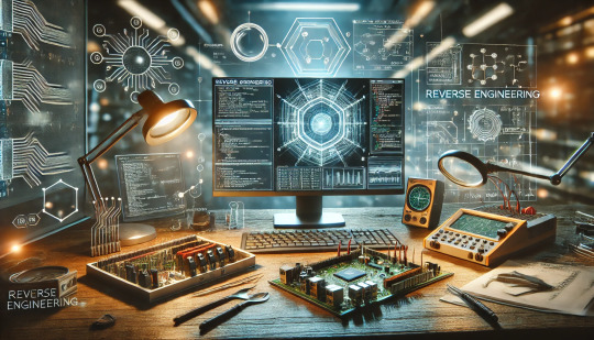
Introduction
Reverse engineering makes products reveal their secrets from inside. By understanding components, systems, and functionality, one can acquire information on how to open up the door to innovation and maximize adaptations of existing designs for novel applications using Reverse Engineering Services.
Why Use Reverse Engineering Services?
Recapture Lost Documentation: Duplicate critical design documents for obsolete products.
Improve Product Design: Identify inefficiencies and improve performance.
Competitor Analysis: Analyzing competitors designs and features of a similar product.
Manufacturing Aids: Designing CAD models and prototypes to make for smooth production.
Customized Solutions: Customize the product as required based on application or market.
Applications of Reverse Engineering Services
Automotive: Develop aftermarkets or upgrade for fitment
Aerospace: Re-crafting older designs with a higher precision
Electronics: Reverse engineering services provide the schematic layout from the PCB, firmware, and components.
Medical Devices: ensuring conformance with regulations and enhancing functionality.
Contact us and join onto innovation through the expertise of our high-class reverse engineering service and customized solutions.
Tools & Technologies of Reverse Engineering Services
3D scanners: capture complex geometries with utmost accuracy.
CAD Software: Converts the physical things into digital, editable models
Specialized Software: Further verifies the designs of the hardware, firmware, and systems.
Benefits of Reverse Engineering Services
Cost Effectiveness: Recycling and upgrading of existing products results in cost savings.
Quick Time to Market: Easy Development Process
Innovative Solution: Sector-specific, tailor-made solution; Be ahead
Conclusion
Reverse Engineering Services has emerged as an essential part of a rapidly growing industry. From each restoration of lost designs, whether it is product customization or competitor analysis, it opens the scope for innovation and efficiency. RhoSigma is at the top of the league in reverse engineering service providers, which can significantly help businesses achieve their goals.
Let innovation break free with world-class reverse engineering services and scalable, secure, and efficient solutions.
0 notes
Text
PCB Repair for Industrial Machinery
Printed Circuit Boards (PCBs) are the heart and soul of modern industrial machinery. They control the operation of various components, ensuring seamless functioning. However, PCBs can malfunction due to various factors, leading to downtime and operational inefficiencies. When it comes to PCB repair for industrial machinery, choosing a reliable and experienced service provider is crucial. Shreemeera Electronic Services, based in Pune, offers comprehensive PCB repair solutions for all types of industrial machinery, including AC DC, Servo, and VFD drives repair services.
Common PCB Failures in Industrial Machinery
PCBs in industrial machinery can fail due to several reasons, including:
Component failures: Individual components on the PCB, such as resistors, capacitors, transistors, and integrated circuits, can malfunction or fail.
Open circuits: Breaks or disconnections in the conductive traces on the PCB can prevent current flow.
Short circuits: When conductive traces come into contact with each other, it can cause excessive current to flow, leading to damage.
Corrosion: Exposure to moisture, chemicals, or high temperatures can cause corrosion on the PCB, affecting its conductivity.
Physical damage: Accidental drops, impacts, or mishandling can cause physical damage to the PCB, leading to fractures or broken traces.
The Importance of Timely PCB Repair
PCB failures can have significant consequences for industrial operations. Downtime caused by faulty PCBs can lead to production losses, increased costs, and decreased efficiency. Therefore, it is essential to address PCB issues promptly to minimize disruptions and maintain optimal performance.
Shreemeera Electronic Services is a leading provider of industrial machine PCB repair services in Pune. With years of experience and expertise, they offer comprehensive solutions to address a wide range of PCB problems. Their team of skilled technicians is equipped with state-of-the-art equipment and diagnostic tools to accurately identify and rectify PCB failures.
Services Offered by Shreemeera Electronic Services
PCB repair and replacement: Shreemeera Electronic Services can repair damaged PCBs or replace faulty components to restore functionality.
PCB inspection and testing: They conduct thorough inspections to identify potential issues and perform diagnostic tests to pinpoint the root cause of problems.
PCB cleaning and maintenance: Regular cleaning and maintenance can help prevent PCB failures and extend their lifespan.
PCB reverse engineering: For obsolete or hard-to-find PCBs, Shreemeera Electronic Services can reverse engineer the board to create a replacement.
Emergency PCB repair: They offer emergency repair services to minimize downtime and ensure rapid restoration of operations.
Why Choose Shreemeera Electronic Services?
Expertise and experience: Their team of technicians has extensive experience in PCB repair for industrial machinery.
State-of-the-art equipment: They use advanced diagnostic tools and equipment for accurate diagnosis and repair.
Quick turnaround time: Shreemeera Electronic Services strives to provide timely repairs to minimize downtime.
Quality assurance: They adhere to strict quality standards to ensure the reliability and performance of repaired PCBs.
Competitive pricing: They offer competitive pricing without compromising on quality.
By choosing Shreemeera Electronic Services for your industrial machine PCB repair needs, you can be confident in their ability to provide reliable and efficient solutions. Their expertise and commitment to customer satisfaction make them a trusted partner for businesses across various industries.
#ac dc drives repair services in pune#industrial machine pcb repair services in pune#pcb repair services in pune#shreemeera electronic services
1 note
·
View note
Text
PCB Clone Services: Precision in Reproduction
What is PCB Cloning?
PCB Clone is the process of creating an exact replica of an existing printed circuit board (PCB). This service is essential when you need to reproduce a board for which the original design files are unavailable. PCB cloning involves reverse engineering the board to generate the necessary data for manufacturing a duplicate.
The Role of PCB Clone Services
PCB Cloning Service are vital in scenarios where you need an identical copy of an electronic circuit board. Whether it’s for replacing obsolete hardware, producing additional units, or creating backups, these services ensure precision in reproduction.

How PCB Cloning Works
1. Initial Analysis
The cloning process begins with a detailed analysis of the original PCB. This includes examining the board’s layout, components, and circuitry. Engineers carefully inspect every detail to ensure accurate replication.
2. Reverse Engineering
After the initial analysis, the reverse engineering phase begins. Engineers trace the circuitry, identify components, and create a schematic of the board. This step is crucial in understanding how the PCB functions.
3. Schematic Capture and Layout Design
Once the reverse engineering is complete, a schematic diagram is created. This diagram serves as a blueprint for the new board. Engineers then use specialized software to design a PCB layout that matches the original.
4. Prototyping and Testing
Before full-scale production, a prototype of the cloned PCB is manufactured. This prototype undergoes rigorous testing to ensure it functions exactly like the original board. Any necessary adjustments are made during this phase.
5. Mass Production
Once the prototype passes all tests, the PCB is ready for mass production. The final product is an exact clone of the original board, ready for use in any application.
Benefits of PCB Cloning Services
• Obsolete Hardware Reproduction: Clone services are ideal for replicating outdated circuit boards, ensuring continued operation of legacy systems.
• Cost-Effective: Cloning is often more cost-effective than redesigning a PCB from scratch.
• Fast Turnaround: PCB cloning services can quickly produce duplicates, reducing downtime for critical systems.
Challenges in PCB Cloning
PCB cloning, while beneficial, is not without its challenges. Complex multilayer boards, proprietary components, and encrypted firmware can complicate the cloning process. Skilled engineers are essential to navigate these obstacles and deliver an accurate clone.
Choosing the Right PCB Clone Service
When selecting a Clone PCB Service, consider factors such as experience, technology, and the ability to handle complex projects. A reliable service provider will ensure that your cloned PCBs meet the highest standards of quality and performance.
Conclusion
PCB cloning services play a crucial role in the electronics industry. Whether for preserving legacy systems or producing additional units, these services provide a reliable solution for duplicating PCBs with precision. With the right expertise, PCB cloning ensures that your electronic systems continue to function smoothly, regardless of the challenges posed by outdated or unavailable designs.
0 notes
Text
Offers Flying Probe (Fixtureless) Test as the Ideal Low Cost Solution - Topscom Technology
With the rapidly increasing complexity of assemblies, electrical verification at the prototype level has become a necessity to meet time-to-market requirements. Flying Probe (or Fixtureless) test allows your engineers to focus their efforts on prototype design verification, instead of debugging process issues. Flying Probe test development is low cost and very fast, making it an ideal tool for prototype verification. There is no fixture to purchase, eliminating costly tooling procurement and allowing the ultimate in flexibility to incorporate design changes. Often used in a combinational strategy with AXI or AOI, Flying Probe allows detection and repair of electrical defects such as wrong parts, reversed parts, missing parts, solder opens, and solder bridges before they are in your engineer hands. Flying Probe at Topscom can help you improve your products time-to-market at the highest possible quality levels. https://is.gd/EWoJq8
PCB SMT assembly, China printed circuit board assembly, China PCB factory, China PCB fabrication, China PCB manufacturing, China PCB board, China PCB manufacturer, China PCB service, China PCB prototype, China PCB supplier, China PCB, PCB China, China PCB online, PCB board, China PCB assembly, PCBA China, China PCB design, PCB assembly, China PCB quote, PCBA, contract manufacturing China, China contract manufacturing, contract manufacturing, China electronic assembly, China electronic manufacturing, electronics manufacturing, electronic board manufacturers, China OEM manufacturing, OEM manufacturing, China cable wire harness assembly
0 notes
Text
PCB Cloning Services: What You Need to Know
Introduction
In the fast-paced world of electronics, staying ahead of the competition often requires innovation and efficiency. PCB cloning services play a pivotal role in achieving this goal. If you're in need of PCB reverse engineering, cloning, or copying services, Circuit Engineering Company Limited is your go-to destination. Explore the world of PCB cloning and discover the exceptional services offered by Circuit Engineering.

What is PCB Cloning?
PCB cloning, also known as PCB reverse engineering, is the process of recreating an existing printed circuit board (PCB) design without access to the original design files. This service is invaluable for various purposes, including product improvement, quality control, and overcoming obsolescence issues. Circuit Engineering specializes in providing top-notch PCB cloning services.
Understanding PCB Cloning Services at Circuit Engineering

Expertise and Experience
Circuit Engineering boasts a team of skilled professionals with years of experience in PCB cloning. They have successfully worked on a wide range of projects, from simple single-layer boards to complex multi-layer designs. This expertise ensures that you'll receive a high-quality and accurate cloned PCB.
State-of-the-Art Technology
Circuit Engineering uses cutting-edge technology and equipment to ensure precision and reliability in the PCB cloning process. Advanced tools and software are employed to analyze and recreate the PCB design, ensuring that the cloned board functions as expected.

Quality Assurance
Quality is paramount in the world of PCB cloning. Circuit Engineering is committed to delivering PCB clones that meet or exceed industry standards. Rigorous testing and quality assurance processes are in place to ensure the reliability and durability of the cloned PCBs.
Cost-Effective Solutions By choosing PCB cloning services from Circuit Engineering, you can save both time and money. Instead of redesigning an entire PCB from scratch, cloning allows you to replicate an existing design accurately, reducing development time and costs.

Versatility
Circuit Engineering's PCB cloning services are highly versatile. Whether you need to clone a single PCB or an entire product line, their team can handle the task efficiently. Their services are suitable for industries such as consumer electronics, aerospace, automotive, and more.
Why Choose Circuit Engineering?
Customer-Centric Approach: Circuit Engineering focuses on understanding your unique requirements and tailoring their services to meet your needs.
Timely Delivery: They recognize the importance of deadlines and work diligently to ensure on-time delivery of cloned PCBs.
Confidentiality: Your intellectual property is safe with Circuit Engineering. They maintain strict confidentiality throughout the cloning process.
Affordable Pricing: Circuit Engineering offers competitive pricing, making their PCB cloning services accessible to a wide range of customers.
Conclusion
If you're in need of PCB cloning, reverse engineering, or copying services, Circuit Engineering Company Limited is your trusted partner. Their expertise, state-of-the-art technology, commitment to quality, and cost-effective solutions make them the best choice for your PCB cloning needs. Discover the world of PCB cloning with Circuit Engineering, and unlock the potential for innovation and efficiency in your electronics projects.
For more information and to explore their services, visit https://www. .com today. Your journey towards top-quality PCB cloning starts here.
Contact Us Circuit Engineering Company Limited
Rm.1902, Easey Comm. Bldg., 253-261 Hennessy Road, Wanchai, Hong Kong. Tel: 86-755-21019972
Fax: 86-755-21019976
Skype: circuitengineer
Whatsapp: 86-13430727446
Contact us via email at: infocircuitengineer.com
#Pcb cloning service#Pcb board cloning service#Circuit board cloning service#Best circuit board cloning service#Pcb clone service#Best pcb board cloning service
0 notes
Text
PCB Manufacture: China vs. US
Looking back on your daily life, have you noticed the growth of consumer electronics and automotive industries are affecting your life and work? Accordingly, it also drives the booming market of PCB Manufacture, which is expected to reach an estimated $89.7 billion by 2024 with a CAGR of 4.3% from 2019 to 2024. Much of this market is currently controlled by PCB manufacturer China companies in places like Shenzhen, which is located in Southeastern China. However, the history of PCB booming in the United States can be traced back to 1950, which is far earlier than China entering this market.
So why can PCB Manufacturer China dominates the market rather than the United States? To solve the confusion for PCB procurements about choosing PCB manufacturer China or US instead, we’ve listed the comparison between the United States and China.
Competitive factors of PCB manufacturer China

According to this report, price was the dominant primary competitive factor in Non-U.S PCB manufacturer, accounting for 76 percent of responses, and China was the leading location, accounting for 67 percent of responses.
And the comparative advantages in various costs which result in lower finished bare PCB prices are:
Labor Costs
Material Costs
Equipment Costs
Environmental Compliance Costs
Building Space Costs
R&D Costs
Supplier Chain
Let’s take Shenzhen MOKO Technology Co., Ltd as an example, which is one of the leading SEM PCB manufacturing and PCB assembly factory in Shenzhen, China.
Labor cost: As you know, Shenzhen is a fast-developing city that gathers many high-tech electronics and automotive industries, each company included MOKO requires clear division of labor, and due to the economic level of China compared to US and easier access to skilled workers, the labor cost of MOKO is far cheaper than in US.
Material cost: MOKO Technology was established since 2001, it’s proficient and experienced in manufacturing PCB and PCB assembly, and also established a stable relationship with accountable material supplier. For a PCB manufacturer that aims to win customers with high-quality and after-sale service, there are many audit processes to certified a material supplier, so the long-term relationship with material suppliers saves a lot of cost of MOKO Technology. Of course, it also doesn’t mean that there’s an opportunity for the material supplier to mix some poor material, from the material sourcing to the forming of substrate and the performance testing of the final products, each process is under strict requirements and testing.
Equipment cost: Chinese high-end equipment is constantly replacing the import, recognized and ordered by the famous PCB enterprises at home and abroad as its high-quality and cost-saving, such as laser drilling machine, laser cutting machine, CNC drilling machine, automatic laser imaging system (LDI), vertical continuous electroplating automatic line (VCP), automatic automatic on and off detection. The main PCB special equipment/instrument representative companies in China are Han’s Laser Technology Industry Group Co., Ltd, Zhengye Technology, UCE Group, Shenzhen Mason Electronics Co., Ltd., and Ta Liang Technology Co., Ltd.
R&D Costs: Due to the overall economic and outcome level in China, the educated and experienced Engineers' salaries and R&D equipment, relevant material and tooling are cheaper than in the US.
Supplier chain: As mass PCB production has shifted away from the U.S. towards Asia,especially Shenzhen, so China has the advantage of the industry supply chain.
Forty-five percent of BIS survey respondents stated that a reduction in U.S. companies that manufacture laminate and other circuit-board related materials has created supply problems for them.
Furthermore, Electronic Contract Manufacturing has been known historically to dramatically reduce supply chain costs, in some cases cutting them in half. ECM has made it possible for companies to shed all or most of their internal manufacturing facilities thereby freeing their valuable company resources for other productive business purposes. In some cases, Electronic Contract Manufacturing has enabled companies to operate without the need for internal manufacturing capabilities or internally-managed factories.
Many companies may choose to outsource their well-established longstanding products to an Electronic Contract Manufacturer, thereby allowing for a greater focus on internal operations for newer products of greater complexity which may have higher margins.
Competitive factors of PCB manufacturer US

According to respondents, U.S. bare PCB manufacturers possess the comparative advantage in:
Lead Time
Quality
Performance
Through the comparison of the advantage between PCB manufacturer China & the US, I believe you’ve got a clear idea for choosing the PCB manufacturer between China and the US, so the next thing you should figure out is what you most concerns when choosing a PCB manufacturer.
Cost
Quality
Lead time
MOQ
Design safety
Experience & Expertise
After-sale service
If you’re considering high-volume production and the price is the most essential factor for your market plan, then you should choose a PCB manufacturer in China as it can save you lots of money for other donate or patronage.
And of course the quality should not be ignored, there are many excellent PCB manufacturers in the US with advanced equipment for ensuring the quality and lead time, and if your company is based on the US, maybe it would be convenient for you to visit the company.
But we know, for business, who don’t want to cooperate with a company that can be conformed to both cost and quality? And of course, to establish your long-term relationship with the PCB manufacturer, most of you would choose to start with a prototype or sample, which is a good way to decrease the deficit and finding out the problem before mass production.
So in such a condition, I suggest you find a reputable and certified experienced PCB manufacturer in China.
Located in Shenzhen, China, MOKO Technology is an expert at PCB Manufacturing and PCB assembly since 2001. MOKO covers an area of more than 8,000 square meters, and has over 250 employees, among them, there are 70 engineers for R&D team and 45 overseas sales for the business team.
Cost:
Firstly, based on geography advantage, MOKO Technology can save a lot of costs like material, component sourcing, labor cost and so on.
Secondly, it has a professional complete procedure from the inquiry to shipping. After receiving the inquiry, MOKO Technology has a team to evaluate customers’ requirements and make an optimized scheme for you, for the material, you will be suggested to choose the suitable material that can perform best for the property.
Thirdly, MOKO Technology has the advantage of supplier chain and it’s experienced in EMS with a one-stop service, which only saves you lots of time and money.
Quality:
For the R&D cost, MOKO Technology has hired experienced 70 engineers
Certified in accordance with ISO 9001: 2015, IPC, and UL (PCB factory: E501497 94V-0; PCB assembly factory: E499341) standards
Bare Board 100 % Visual Inspection & AQL on mechanical to IPC-600 Class II or III
Assembly 100% Visual Inspection to IPC-610 Class II or III
Polar TDR Impedance Testing
PCB Board Net List Electrical Testing 100%
Micro-section Evaluation and Reports
PCB Assembly – ICT testing
PCB Assembly – Functional Testing
PCB Assembly – Burn-In-Testing
X-ray for PC board registration
X-ray for BGA and Component Verification
Automated Optical Inspection (AOI)
Lead Time of PCB Assembly:
MOKO provide 2-50 layered PCBs for fabrication, including HDI, Rigid, Rigid-Flex, & flex boards. From low quantity to mass production, with high quality, and quick turn available at a low cost.
And for the monthly capacity, it can manufacturer 30,000 square meters PCB and 400,000 pcs.

There’s no minimum order requirement, and for the sample, MOKO Technology can accept 10 pcs as MOQ.
Design safety:
About this issue, you can never worry about it as MOKO Technology will sign DOD Contracts with ITAR Registered
After-sale service:
Online Tracking
ERP Systematic order process, you can check the production status of the entire purchase order, and the whole product cycle time.
Professional sales:
Whatever problems happening, you can be replied within 24 hours. There are 70 engineers to support you, including PCB design & PCB Layout, hardware design engineering, firmware & software development, and personalization.
One pair one timely customer order status feedback
MOKO Technology Ltd is a premiere turn-key PCB assembly manufacturer. We are dedicated to providing the best client service in the electronics manufacturing business. Your total satisfaction is extremely important to us. We will meet all your needs in PCB design and layout, PCB manufacturing, and circuit board assembly
Products application industries1> LED PCB
MOKO Technology can offer one-stop service for led light electronic parts focusing on ODM/OEM led PCBA, OEM LED control PCBA and OEM LED Driver PCBA.
It can design hardware, firmware, iOS/Android APP, plastic. If you have a Gerber file and BOM list, they also can offer OEM service for you.
What can MOKO Technology do for LED project:
PCB Design & Layout
Reverse Engineering Service
Fast PCB&PCBA Prototyping
Components sourcing
PCB Assembly
Cable, Wire Assemblies, and Housing Assemblies
Cover coating and glue
Loading firmware & function testing and Aging testing
ODM/OEM LED PCBA Service:
MOKO Technology produced lots of led PCBA, for example, UV LED PCBA for medical machine, UV LED PCBA for 3D printer, AC220V driverless led PCBA, AC110V driverless led PCBA, LED PCBA for street light, LED PCBA for tube light, LED PCBA for panel light, COB RGB LED PCBA for pool light, RGB LED PCBA for pixel light, LED PCBA for ceiling light, LED PCBA for traffic light, etc.
LED PCBA Design & Layout Cases:

MOKO Technology Ltd is a highly respected telecom PCB Assembly, telecom PCBA Manufacturer specializing in prototyping and small volume building in the highly complex area or telecom and industrial computing Printed Circuit Board Assembly(PCBA), PCB Assembly, PCB Assembly service for leading OEMs.
Telecom Printed Circuit Boards Applications:
Phone switching systems
Signal boost online systems
Cell transmission and tower electronics
Satellite technology High-speed routers and servers
Wireless industrial and commercial phone technology
Space communications technology
Military communications systems
Video collaboration Information security technology
PBX systems Voice over internet protocol
Latest Telecom PCBA Cases:

To ensure a positive response from “end”-consumers, many customers from MOKO build on the quality and reliability provided from MOKO.
Latest Consumer Electronics PCBA Cases:

MOKO offers world-class, custom-designed solutions for the automotive market including rapid prototyping, test and product development support with the highest level of quality and traceability to meet your unique requirements.
Latest Automotive PCBA Cases:

MOKO Technology Ltd specializes in the medical PCB assembly and medical PCB production for medical companies of all sizes.
The workmanship of MOKO Technology Ltd can be found in many medical devices such as diagnostic imaging equipment, lasers, and handheld dental tools.
Latest Medical PCBA Cases:

For several years, MOKO has worked with a variety of customers in the industrial market segment from sensors, conditioning systems for alternative energy, power monitoring systems, industrial controls as well as others with demanding environmental requirements.
Latest Industrial PCBA Cases:

So after all this research above, I think choosing the most suitable PCB manufacturer according to your concern is a wise choice. Whatever it’s PCB manufacturer China or PCB manufacturer US, make sure you’ve been clear about your concerns and know your supplier well!
For more info about MOKO Technology Co., Ltd, you can visit https://www.mokotechnology.com/
1 note
·
View note
Text

Get Simplified PCB Reverse Engineering at SZOROD Learn the secrets of reverse engineering with SZOROD. With 20 years of expertise, we’ve mastered handling complicated multi-layer boards with blind holes and unlocking challenging IC chips. Our PCB reverse engineering service ensures high-quality product enhancement and cost savings. Benefit from our 100% success rate in PCB board copying, modification, schematic diagram derivation, BOM list creation, and PCB production. At SZOROD, we guarantee transparency and reliability. Try us for quick and accurate reverse engineering solutions. https://pcb-reverse-engineering.com/
0 notes
Text
What to Look for in an EMS Provider in India & Why India Is Emerging as a Global Hub
Choosing the right electronics manufacturing services (EMS) provider in India is crucial for any company looking to scale its hardware production efficiently and cost-effectively. Whether a startup launching a new device or an established business optimizing your supply chain, partnering with a reliable EMS provider can make or break your product journey.
In recent years, India has emerged as a competitive and technologically advanced hub for electronics manufacturing. With government initiatives like “Make in India,” a growing talent pool, and robust infrastructure, the country is positioning itself as a global leader.
In this answer, I’ll explain the key factors to consider when selecting an EMS provider in India and why India is gaining international attention in the electronics manufacturing sector.
Key Qualities to Look for in an EMS Provider in India
1) End-to-End Capabilities: Look for a company that provides comprehensive services—from prototyping and PCB assembly to final product assembly, testing, and packaging. An integrated approach ensures better communication, faster turnaround, and lower costs.
2) Advanced Infrastructure & Technology: The provider should have modern manufacturing facilities equipped with surface mount technology (SMT) lines, automated optical inspection systems, X-ray inspection, and cleanroom environments if necessary. This ensures precision and scalability.
3) Certifications & Quality Standards: A reputable electronics manufacturing services provider in India should have internationally recognized certifications such as ISO 9001, ISO 14001, and IPC standards. This ensures the products meet global quality and safety norms.
4) Customization & Flexibility: Whether you're working with a small batch or a mass production order, the provider must be agile enough to adapt to your volume needs. Ask if they offer engineering support for design for manufacturing (DFM) to improve efficiency and reduce costs.
5) Component Sourcing Capabilities: Efficient sourcing of components, especially during global supply chain shortages, is a big advantage. Established EMS companies have vendor relationships and procurement teams that ensure reliable sourcing at competitive rates.
6) Experience & Industry Focus: Look for companies with experience in your sector—consumer electronics, medical devices, automotive electronics, IoT, or industrial applications. Industry-specific knowledge can improve compliance and functionality.
7) Communication & Project Management: Effective collaboration is vital. Evaluate their communication channels, reporting frequency, and project management tools. You want a provider who acts like a partner, not just a vendor.
8) Post-Production Services: Value-added services such as after-sales support, repair, maintenance, and reverse logistics can enhance customer experience and reduce lifecycle costs.
Why India Is Becoming a Preferred Destination for EMS
1) Cost Advantage: Manufacturing in India offers lower operational and labor costs than Western countries and other Asian competitors like China. This makes Indian EMS providers extremely attractive for global brands.
2) Skilled Workforce: India produces thousands of engineering graduates annually, many specializing in electronics and communications. This talent pool supports innovation and high-quality output.
3) Government Support: The Indian government’s Production Linked Incentive (PLI) scheme for electronics manufacturing draws domestic and international investments. Regulatory reforms and tax incentives also contribute to a business-friendly environment.
4) Strategic Location: Geographically, India serves as a gateway between the East and the West. For companies looking to distribute in both regions, India offers logistical advantages.
5) Robust Domestic Demand: With a population of over 1.4 billion and increasing digital adoption, India represents a massive electronics market. EMS providers benefit from this dual opportunity of domestic and export markets.
6) Sustainability & Compliance Focus: Many Indian EMS firms adopt green manufacturing practices and comply with global environmental standards like RoHS and WEEE, aligning with ESG-conscious companies.
Resolute GOC – A Prominent EMS Provider in India
One leading name in the industry is Resolute GOC, a full-service electronics manufacturing services provider in India. With advanced infrastructure, a customer-centric approach, and a focus on precision, Resolute GOC supports industries ranging from telecom and defense to healthcare and consumer electronics.
They provide solutions that cover every stage of the manufacturing lifecycle, ensuring scalability, accuracy, and time-to-market efficiency. Whether you're looking for PCB assembly, turnkey solutions, or custom-built components, they bring technical expertise and operational excellence.
Final Thoughts
Partnering with the right EMS provider is a strategic decision that affects your product quality, time-to-market, and cost efficiency. India offers a compelling value proposition due to its skilled talent, favorable policies, and advanced manufacturing ecosystem.
When evaluating an electronics manufacturing services provider in India, always prioritize transparency, technical expertise, and adaptability. Don’t just compare quotes—assess their track record, certifications, technology, and communication style.
With the right EMS partner by your side, you can focus on innovation and go-to-market strategies while they take care of the engineering and execution behind the scenes.
Have more questions about choosing the right EMS provider in India?
Drop them below, happy to help you navigate the options!
1 note
·
View note
Text
PCB Manufacturer China and PCB Manufacturer US
Looking back on your daily life, have you noticed the growth of consumer electronics and automotive industries are affecting your life and work? Accordingly, it also drives the booming market of PCB Manufacture, which is expected to reach an estimated $89.7 billion by 2024 with a CAGR of 4.3% from 2019 to 2024. Much of this market is currently controlled by PCB manufacturer China companies in places like Shenzhen, which is located in Southeastern China. However, the history of PCB booming in the United States can be traced back to 1950, which is far earlier than China entering this market.
So why can PCB Manufacturer China dominates the market rather than the United States? To solve the confusion for PCB procurements about choosing PCB manufacturer China or US instead, we’ve listed the comparison between the United States and China.
Competitive factors of PCB manufacturer China

According to this report, the price was the dominant primary competitive factor in Non-U.S PCB manufacturer, accounting for 76 percent of responses, and China was the leading location, accounting for 67 percent of responses.
And the comparative advantages in various costs which result in lower finished bare PCB prices are:
Labor Costs
Material Costs
Equipment Costs
Environmental Compliance Costs
Building Space Costs
R&D Costs
Supplier Chain
Let’s take Shenzhen MOKO Technology Co., Ltd as an example, which is one of the leading SEM PCB manufacturing and PCB assembly factory in Shenzhen, China.
Labor cost: As you know, Shenzhen is a fast-developing city that gathers many high-tech electronics and automotive industries, each company included MOKO requires clear division of labor, and due to the economic level of China compared to US and easier access to skilled workers, the labor cost of MOKO is far cheaper than in US.
Material cost: MOKO Technology was established since 2001, it’s proficient and experienced in manufacturing PCB and PCB assembly, and also established a stable relationship with accountable material supplier. For a PCB manufacturer that aims to win customers with high-quality and after-sale service, there are many audit processes to certified a material supplier, so the long-term relationship with material suppliers saves a lot of cost of MOKO Technology. Of course, it also doesn’t mean that there’s an opportunity for the material supplier to mix some poor material, from the material sourcing to the forming of a substrate and the performance testing of the final products, each process is under strict requirements and testing.
Equipment cost: Chinese high-end equipment is constantly replacing the import, recognized and ordered by the famous PCB enterprises at home and abroad as its high-quality and cost-saving, such as laser drilling machine, laser cutting machine, CNC drilling machine, automatic laser imaging system (LDI), vertical continuous electroplating automatic line (VCP), automatic automatic on and off detection. The main PCB special equipment/instrument representative companies in China are Han’s Laser Technology Industry Group Co., Ltd, Zhengye Technology, UCE Group, Shenzhen Mason Electronics Co., Ltd., and Ta Liang Technology Co., Ltd.
R&D Costs: Due to the overall economic and outcome level in China, the educated and experienced Engineers' salaries and R&D equipment, relevant material and tooling are cheaper than in the US.
Supplier chain: As mass PCB production has shifted away from the U.S. towards Asia,especially Shenzhen, so China has the advantage of the industry supply chain.
Forty-five percent of BIS survey respondents stated that a reduction in U.S. companies that manufacture laminate and other circuit-board related materials has created supply problems for them.
Furthermore, Electronic Contract Manufacturing has been known historically to dramatically reduce supply chain costs, in some cases cutting them in half. ECM has made it possible for companies to shed all or most of their internal manufacturing facilities thereby freeing their valuable company resources for other productive business purposes. In some cases, Electronic Contract Manufacturing has enabled companies to operate without the need for internal manufacturing capabilities or internally-managed factories.
Many companies may choose to outsource their well-established longstanding products to an Electronic Contract Manufacturer, thereby allowing for a greater focus on internal operations for newer products of greater complexity which may have higher margins.
Competitive factors of PCB manufacturer US

According to respondents, U.S. bare PCB manufacturers possess the comparative advantage in:
Lead Time
Quality
Performance
Through the comparison of the advantage between PCB manufacturer China & the US, I believe you’ve got a clear idea for choosing the PCB manufacturer between China and the US, so the next thing you should figure out is what you most concern when choosing a PCB manufacturer.
Cost
Quality
Lead time
MOQ
Design safety
Experience & Expertise
After-sale service
If you’re considering high-volume production and the price is the most essential factor for your market plan, then you should choose a PCB manufacturer in China as it can save you lots of money for other donate or patronage.
And of course the quality should not be ignored, there are many excellent PCB manufacturers in the US with advanced equipment for ensuring the quality and lead time, and if your company is based on the US, maybe it would be convenient for you to visit the company.
But we know, for business, who don’t want to cooperate with a company that can be conformed to both cost and quality? And of course, to establish your long-term relationship with the PCB manufacturer, most of you would choose to start with a prototype or sample, which is a good way to decrease the deficit and finding out the problem before mass production.
So in such a condition, I suggest you find a reputable and certified experienced PCB manufacturer in China.
Located in Shenzhen, China, MOKO Technology is an expert at PCB Manufacturing and PCB assembly since 2001. MOKO covers an area of more than 8,000 square meters, and has over 250 employees, among them, there are 70 engineers for R&D team and 45 overseas sales for the business team.
Cost:
Firstly, based on geography advantage, MOKO Technology can save a lot of costs like material, component sourcing, labor cost and so on.
Secondly, it has a professional complete procedure from the inquiry to shipping. After receiving the inquiry, MOKO Technology has a team to evaluate customers’ requirements and make an optimized scheme for you, for the material, you will be suggested to choose the suitable material that can perform best for the property.
Thirdly, MOKO Technology has the advantage of supplier chain and it’s experienced in EMS with a one-stop service, which only saves you lots of time and money.
Quality:
For the R&D cost, MOKO Technology has hired experienced 70 engineers
Certified in accordance with ISO 9001: 2015, IPC, and UL (PCB factory: E501497 94V-0; PCB assembly factory: E499341) standards
Bare Board 100 % Visual Inspection & AQL on mechanical to IPC-600 Class II or III
Assembly 100% Visual Inspection to IPC-610 Class II or III
Polar TDR Impedance Testing
PCB Board Net List Electrical Testing 100%
Micro-section Evaluation and Reports
PCB Assembly – ICT testing
PCB Assembly – Functional Testing
PCB Assembly – Burn-In-Testing
X-ray for PC board registration
X-ray for BGA and Component Verification
Automated Optical Inspection (AOI)
Lead Time of PCB Assembly:
MOKO provides 2-50 layered PCBs for fabrication, including HDI, Rigid, Rigid-Flex, & flex boards. From low quantity to mass production, with high quality, and quick turn available at a low cost.
And for the monthly capacity, it can manufacturer 30,000 square meters PCB and 400,000 pcs.

There’s no minimum order requirement, and for the sample, MOKO Technology can accept 10 pcs as MOQ.
Design safety:
About this issue, you can never worry about it as MOKO Technology will sign DOD Contracts with ITAR Registered
After-sale service:
Online Tracking
ERP Systematic order process, you can check the production status of the entire purchase order, and the whole product cycle time.
Professional sales:
Whatever problems happening, you can be replied within 24 hours. There are 70 engineers to support you, including PCB design & PCB Layout, hardware design engineering, firmware & software development, and personalization.
One pair one timely customer order status feedback
MOKO Technology Ltd is a premiere turn-key PCB assembly manufacturer. We are dedicated to providing the best client service in the electronics manufacturing business. Your total satisfaction is extremely important to us. We will meet all your needs in PCB design and layout, PCB manufacturing, and circuit board assembly
Products application industries1> LED PCB
MOKO Technology can offer one-stop service for led light electronic parts focusing on ODM/OEM led PCBA, OEM LED control PCBA and OEM LED Driver PCBA.
It can design hardware, firmware, iOS/Android APP, plastic. If you have a Gerber file and BOM list, they also can offer OEM service for you.
What can MOKO Technology do for LED project:
PCB Design & Layout
Reverse Engineering Service
Fast PCB&PCBA Prototyping
Components sourcing
PCB Assembly
Cable, Wire Assemblies, and Housing Assemblies
Cover coating and glue
Loading firmware & function testing and Aging testing
ODM/OEM LED PCBA Service:
MOKO Technology produced lots of led PCBA, for example, UV LED PCBA for medical machine, UV LED PCBA for 3D printer, AC220V driverless led PCBA, AC110V driverless led PCBA, LED PCBA for street light, LED PCBA for tube light, LED PCBA for panel light, COB RGB LED PCBA for pool light, RGB LED PCBA for pixel light, LED PCBA for ceiling light, LED PCBA for traffic light, etc.
LED PCBA Design & Layout Cases:

MOKO Technology Ltd is a highly respected telecom PCB Assembly, telecom PCBA Manufacturer specializing in prototyping and small volume building in the highly complex area or telecom and industrial computing Printed Circuit Board Assembly(PCBA), PCB Assembly, PCB Assembly service for leading OEMs.
Telecom Printed Circuit Boards Applications:
Phone switching systems
Signal boost online systems
Cell transmission and tower electronics
Satellite technology High-speed routers and servers
Wireless industrial and commercial phone technology
Space communications technology
Military communications systems
Video collaboration Information security technology
PBX systems Voice over internet protocol
Latest Telecom PCBA Cases:

To ensure a positive response from “end”-consumers, many customers from MOKO build on the quality and reliability provided from MOKO.
Latest Consumer Electronics PCBA Cases:

MOKO offers world-class, custom-designed solutions for the automotive market including rapid prototyping, test and product development support with the highest level of quality and traceability to meet your unique requirements.
Latest Automotive PCBA Cases:

MOKO Technology Ltd specializes in the medical PCB assembly and medical PCB production for medical companies of all sizes.
The workmanship of MOKO Technology Ltd can be found in many medical devices such as diagnostic imaging equipment, lasers, and handheld dental tools.
Latest PCBA Cases:

For several years, MOKO has worked with a variety of customers in the industrial market segment from sensors, conditioning systems for alternative energy, power monitoring systems, industrial controls as well as others with demanding environmental requirements.
Latest Industrial PCBA Cases:

So after all this research above, I think choosing the most suitable PCB manufacturer according to your concern is a wise choice. Whatever it’s PCB manufacturer China or PCB manufacturer US, make sure you’ve been clear about your concerns and know your supplier well!
For more info about MOKO Technology Co., Ltd, you can visit https://www.mokotechnology.com/ and https://www.mokotechnology.com/pcb-manufacturer-china-vs-us/
1 note
·
View note
Text
5 Benefits Of Building Prototype Circuit Boards
A Printed Circuit Board (PCB) Prototype is a physical representation of a printed circuit board design. PCB prototyping is a crucial phase in the manufacture of PCBs. In this post, we will discuss some reasons why you should create PCB prototypes. Let’s get started.

A cost-effective way to test a PCB design
By creating a working model of the circuit board in a test environment, designers can quickly evaluate the board’s performance. This allows them to make necessary adjustments before committing to a full production run. As a result, designers can save time, and the customer avoids having to pay for numerous production runs.
Allows designers to refine the boards
A prototype enables designers to quickly identify any design flaws or areas for improvement and make changes to their design before producing the final product. This way, they can create a more efficient and reliable product with fewer errors.
Testing of new components and technologies
By testing a prototype in a controlled environment, designers can evaluate the performance of new components. It’s a great way to determine whether the new components will work correctly in the final product.
Verify component placement
A PCB prototype allows you to verify the placement of components on the board. This is vital because incorrect placement can lead to issues such as interference, noise, and heat dissipation problems.
Faster time to market
Building a prototype circuit board leads to faster time to market. By testing and validating the design beforehand, engineers can ensure that the final product meets the necessary requirements and standards. This helps businesses to bring their products to market faster, gaining a competitive advantage over other businesses in the industry.
A top-quality PCB Prototype service
Bay Area Circuits(BAC) is the leading prototype circuit board manufacturer in the United States. We have been in the industry for over four decades and have the knowledge and experience to build excellent PCB prototypes. With the help of tools like DFX to Gerber converter and DipTrace designer, we can create high-quality prototypes. What’s more, we can do reverse engineering PCB. Do you want to build a PCB prototype for your project? Contact us to request a quote.
View the original source here: medium.com/@bayareacircuitsusa/5-benefits-of-building-prototype-circuit-boards-c4c5f0e4fe3e
0 notes