#Transistor Array
Explore tagged Tumblr posts
Visit Tumblr Blog
Explore Tumblr blogs with no restrictions, modern design and the best experience.
Last Seen Tumblr Blogs


Fun Fact
There are dozens of funny blogs to kill time on Tumblr.
Text
High Voltage Darlington Array, Darlington array led, Transistor Array
ULN Series 50V 500 mA High Voltage High Current Seven Darlington Array - SOIC-16
0 notes
Text
https://www.futureelectronics.com/p/semiconductors--discretes--transistors--mosfets/irf4905strlpbf-infineon-8173863
Mosfet applications, high voltage mosfet, Mosfet applications, mosfet switch
Single P-Channel 55 V 0.02 Ohm 180 nC HEXFET® Power Mosfet - D2PAK
#Transistors#Mosfets#IRF4905STRLPBF#Infineon#applications#high voltage mosfet#Mosfet applications#transistor mosfet#audio#mosfet module#transistor#mosfet gate#Power mosfet#mosfet electronics#ESD protection arrays
1 note
·
View note
Text
MMPQ6502 BK Bipolar Transistor Arrays with an exclusive discount by SUV System Ltd

A leading electronic component supplier in China, is rolling out SPECIAL DISCOUNTS on their hottest selling #semiconductordevices
With offices in Hong Kong and Shenzhen, and a fully stocked product warehouse, we offer a wide range of products from leading brands.
For queries, Contact us at [email protected]
Skype: [email protected]
To purchase this product, click https://www.suvsystem.com/en/plDK277pi/MMPQ6502%20BK.html
0 notes
Text
Perfect Speakers
What do I know about the perfect speaker, lots actually.
You see I have built them 4 times. First task is perfect as a concept must be defined. Then a plan that embodies the idea is established. Then you build the sucker.
My first attempt was a big electrostatic. Electrostatic speakers are great everyone says so. Fast accurate and dynamic. Compared to "Statics" cone drivers are dull and slow. Ask anyone. As a first try it seems rather ambitious. Mechanically they are actually very simple. You need a couple of sheets of perforated steel, a mylar membrane, and some plastic strips. You build a layer cake of Steel, plastic strips, Mylar, more strips, and a final layer of steel.
Try making a cone loudspeaker driver in the basement without a lot of weird tools.
There are two tricky bits. One is you have to make the Mylar conductive. In my case I spread a layer of graphite I got from drafting pencil sharpeners. (I did drafting ). The other tricky bit is getting impedance matching transformers to make the hundreds of volts needed to drive the stators which is what the steel sheets are called.
For the actual speaker array I made three panels one foot wide four feet tall and mounted them side by side in a wooden frame. The two on each side were canted out a bit. One such array per channel.
I decided that rather that looking for just transformers I would buy a pair of Tube amplifiers. They had transformers that were audio grade already. Oh and then I could attach the stators directly to the primary windings of the amp for a direct coupled drive. If you know what that means you may even be impressed. I had two problems with that. first is that tube amps were going into the trash more often than the used market, (50 years ago) and I had to rejig the feedback in the amp which came off the secondary winding.
The most amazing thing was I got all this done and it worked. It worked really well. It was perfect and my friends were impressed. My future wife was impressed. (that early exposure to my hobby made her tolerant of my later adventures)
It was great, but.....
Even big electrostatics have funny Bass. Phase cancellation and sounds bouncing around the room were a problem. Not as perfect as legend has them. I added a subwoofer driven by a transistor amp (the HK 12 I still have) That helped, but satisfaction was not to be found. When you have doubts about perfection it is serious.
The experience of two moves with big awkward speaker things eventually to a too small apartment made the situation impossible. I disassembled them and put the parts in storage. (I still have most of them)
The idea of perfection changed. Easier to live with and must fit comfortably in a living room. Hmmmm. Next set was a small pair of boxes using a nice 4 inch woofer I found that was almost full range. It reproduced the human voice with uncanny realism. I put a pair in a tuned box with a tweeter and it worked fine. Small apartment problem solved. It had better bass than the "Statics."
Later we moved into a house. Small boxes are small. I like big music.
Hmmm....
How about taking the nice tiny woofers that sounded so good and using 4 per side, and add a 12" woofer underneath. Biamp the sucker yes that's the idea. I had a wood shop build me the boxes. Tall pyramidal obelisks with 6 divers, bi-amped. ( That Citation 12 was sure handy)
It sounded really good. It filled the room with big sound, yet the human voice was scary real and the timbre of woodwinds was to die for. It resembles a lot of high end beasts sold today. I still have them as the front end of my Video surround setup.
All this time my main amps were the same tube amps I bought years before. They were Dynaco Mk3s, 60 Watts per side, and really easy to upgrade and improve. We had little kids and hot high voltage devices on the floor were a bit scary.
I built a transistor amp from a kit of leftover parts when Dynaco shut down. That is the Franken amp. Less scary and pretty resistant to curious fingers of small kids.
We moved a couple more times, eventually to a nice small house. My wife was patient for a while with the obelisks in the living room but the size was almost oppressive. A couch a chair and a BIG stereo. It was a stereotypical setup and a problem even for me. The compromise was to put the stereo away and use the monster speakers in the AV system downstairs to watch videos with spectacular surround sound. No fragile turntable to damage with bigger kids and their friends. Video Tape, CDs and DVDs were the thing. "Why do you keep all those albums you haven't played them for years?"
The kids got bigger and more responsible and trustworthy. I wanted my old stereo back. I wanted to play my albums.
I had a new idea. There was an ad in craiglist for a strange speaker from Denmark I think. It did not look like a conventional speaker. I had heard a set decades ago. Damn, it sold fast, someone else recognized it. But I could build a set like that. Smallish, modest dimensions and designed to go hard against a wall. Take advantage of Bass reinforcement using a wall and the floor. Tune the box with those cool equations and design a cross-over with a computer program. I knew where to buy good components.
I could make a better version of that Scandinavian set.
So some nice birch plywood, some high end drivers, and some actually rather expensive inductors and capacitors were purchased. I had some decent carpentry skills by now and a few power tools. I ended up with some nice boxes with a natural blonde oil finish. They look good and actually they do not look at all like speakers unless you look hard. I call them stealth. Oh and they sound really good. The best yet.
Better than direct coupled large electrostatics. Better that small boxes. Better than big obelisks. Better than all those. The wife likes them. They are perfect.
#audiophile#high end audio#Perfect Speakers#stereo speakers#Build them speakers#audioblr#cheap audiophile#tubes vs transistors#Hifi#Hi Fi#stereo#Hi Fi Stereo
2 notes
·
View notes
Text
### Report on the Ancient Cogitator
#### Found in the Depths of Mars
**By the Omnissiah’s Grace, Servant of the Machine God, Tech Priest Dominus Pdep Eith**
---
**Date: M39.305**
**Subject: Cogitator Designation – Unknown**
---
In the year of the Omnissiah M42.305, an expedition into the subterranean vaults beneath the surface of Mars did yield a most wondrous find: an ancient cogitator of unknown origin, long lost to the sands of time. This device, encrusted with the dust of millennia, hath been identified through the holy rites of tech-retrieval as a device of remarkable antiquity. By the will of the Machine God, I do hereby present a thorough account of its features and internal layout.
#### External Features
The exterior of this venerable cogitator doth present itself in a rectangular form, wrought from a durable metal alloy that hath withstood the ravages of countless ages. The surface is adorned with an array of switches and lights, each one a testament to the artisanship of ancient tech-priests. The face of the cogitator is dominated by a control panel, bedecked with a myriad of toggle switches, rotary controls, and luminescent indicators.
- **Dimensions:** Approximately three feet in height, two feet in width, and a foot in depth.
- **Material:** Sturdy alloy, resistant to corrosion and wear.
- **Interface:** An array of manual switches and indicator lights for direct interaction.
#### Internal Layout
Upon delving into the inner sanctum of the cogitator, the sacred architecture reveals itself in a manner most intricate. The internal layout is a marvel of ancient engineering, exhibiting a modular design that doth allow for ease of access and maintenance by those initiated in the rites of tech-repair.
- **Processing Unit:** The heart of the cogitator, the Central Processing Unit (CPU), is a compact assembly of transistors and circuits. It doth operate at a clock speed of 1 MHz, a relic by today’s standards, yet a marvel of its time.
- **Memory:** The cogitator doth possess a core memory of 4,096 words, each word being twelve bits in length. This magnetic core memory is both robust and reliable, providing swift access to data.
- **Input/Output Modules:** The cogitator is equipped with various I/O modules, allowing for the connection of peripheral devices. These modules are interfaced via a backplane, a unifying structure of interconnecting circuits.
- **Power Supply:** The power sanctum of the cogitator is a robust unit, designed to convert and regulate energy, ensuring the smooth operation of the cogitator’s components.
#### Operational Characteristics
The operational rites of the cogitator are governed by a series of machine instructions, simple yet powerful in their execution. The instruction set architecture is designed to perform a variety of computational tasks with efficiency and precision.
- **Instruction Set:** Comprising a minimalistic set of operations, including basic arithmetic, logic, control flow, and data manipulation instructions.
- **Programming:** The cogitator is programmable via electro-arcana script, each instruction directly corresponding to a machine operation.
- **Performance:** While humble by the standards of our current sacred machinery, the cogitator performs its designated tasks with admirable fidelity and speed.
#### Conclusion
In the name of the Omnissiah, the rediscovery of this ancient cogitator doth enrich our understanding of the ancient ways. This cogitator, a relic of a bygone era, stands as a testament to the ingenuity and craftsmanship of those who came before us. As we venerate the Machine God, let us continue to unearth and study such treasures, that we may preserve the sacred knowledge and further the glory of the Adeptus Mechanicus.
By the will of the Omnissiah and the blessings of the Machine God, this report is thus concluded.
**Ave Deus Mechanicus.**

7 notes
·
View notes
Text
Undergrad research blast from the past. Here I am in 2020 assembling a micro fluidic flow cell with a gold electrode block. I think I took this video for myself so I knew what to clip to what. This was when I worked with electrochemical sensors, transducing signals via impedance spectroscopy.
A lot of electrochemical techniques rely on measuring voltages or currents, but in this lab we looked at impedance- which is a fancy combination of regular resistance (like the same one from ohms law) and the imaginary portion of the resistance that arises from the alternating current we supply.
I would functionalize different groups on the gold working electrode by exposing the surface to a solution of thiolated biomarker capture groups. Thiols love to form self-assembled mono layers over gold, so anything tagged with thiol ends up sticking. [Aside: Apparently after I left the group they moved away from gold thiol interactions because they weren't strong enough to modify the electrode surface in a stable and predictable way, especially if we were flowing the solution over the surface (which we wanted to do for various automation reasons)]. The capture groups we used were various modified cyclodextrins- little sugar cups with hydrophobic pockets inside and a hydrophilic exterior. Cyclodextrins are the basis of febreeze- a cyclodextrin spray that captures odor molecules in that hydrophobic pocket so they can't interact with receptors in your nose. We focused on capturing hydrophobic things in our little pocket because many different hydrophobic biomarkers are relevant to many different diseases, but a lot of sensors struggle to interact with them in the aqueous environment of bodily fluids.
My work was two fold:
1) setting up an automated system for greater reproducibility and less human labor. I had to figure out how to get my computer, the potentiostat (which controls the alternating current put in, and reads the working electrode response), the microfluidic pump, and the actuator that switched between samples to all talk to each other so I could set up my solutions, automatically flow the thiol solution for an appropriate time and flow rate to modify the surface, then automatically flow a bio fluid sample (or rather in the beginning, pure samples of specific isolated biomarkers, tho their tendency to aggregate in aqueous solution may have changed the way they would interact with the sensor from how they would in a native environment, stabilized in blood or urine) over the electrode and cue the potentiostat for multiple measurements, and then flow cleaning solutions to clean out the tubings and renew the electrode. This involved transistor level logic (pain) and working with the potentiostat company to interact with their proprietary software language (pain) and so much dicking around with the physical components.
2) coming up with new cyclodextrin variants to test, and optimizing the parameters for surface functionalization. What concentrations and times and flow rates to use? How do different groups around the edge of the cyclodextrin affect the ability to capture distinct classes of neurotransmitters? I wasn't working with specific sensors, I was trying to get cross reactivity for the purpose of constructing nonspecific sensor arrays (less akin to antibody/antigen binding of ELISAs and more like the nonspecific combinatorial assaying you do with receptors in your tongue or nose to identify "taste profiles" or "smell profiles"), so I wanted diverse responses to diverse assortments of molecules.
Idk where I'm going with this. Mostly reminiscing. I don't miss the math or programming or the physical experience of being at the bench (I find chemistry more "fun") but I liked the ultimate goal more. I think cross reactive sensor arrays and principle component analysis could really change how we do biosample testing, and could potentially be useful for defining biochemical subtypes of subjectively defined mental illnesses.... I think that could (maybe, possibly, if things all work and are sufficiently capturing relevant variance in biochemistry from blood or piss or sweat or what have you) be a more useful way to diagnose mental illness and correlate to possible responses to medications than phenotypic analysis/interviews/questionnaires/trial and error pill prescribing.
4 notes
·
View notes
Text


NASA’s Europa Clipper Gets Set of Super-Size Solar Arrays
The largest spacecraft NASA has ever built for planetary exploration just got its ‘wings’ — massive solar arrays to power it on the journey to Jupiter’s icy moon Europa.
NASA’s Europa Clipper spacecraft recently got outfitted with a set of enormous solar arrays at the agency’s Kennedy Space Center in Florida. Each measuring about 46½ feet (14.2 meters) long and about 13½ feet (4.1 meters) high, the arrays are the biggest NASA has ever developed for a planetary mission. They have to be large so they can soak up as much sunlight as possible during the spacecraft’s investigation of Jupiter’s moon Europa, which is five times farther from the Sun than Earth is.
The arrays have been folded up and secured against the spacecraft’s main body for launch, but when they’re deployed in space, Europa Clipper will span more than 100 feet (30.5 meters) — a few feet longer than a professional basketball court. The “wings,” as the engineers call them, are so big that they could only be opened one at a time in the clean room of Kennedy’s Payload Hazardous Servicing Facility, where teams are readying the spacecraft for its launch period, which opens Oct. 10.
Flying in Deep Space
Meanwhile, engineers continue to assess tests conducted on the radiation hardiness of transistors on the spacecraft. Longevity is key, because the spacecraft will journey more than five years to arrive at the Jupiter system in 2030. As it orbits the gas giant, the probe will fly by Europa multiple times, using a suite of science instruments to find out whether the ocean underneath its ice shell has conditions that could support life.
Powering those flybys in a region of the solar system that receives only 3% to 4% of the sunlight Earth gets, each solar array is composed of five panels. Designed and built at the Johns Hopkins Applied Physics Laboratory (APL) in Laurel, Maryland, and Airbus in Leiden, Netherlands, they are much more sensitive than the type of solar arrays used on homes, and the highly efficient spacecraft will make the most of the power they generate.
At Jupiter, Europa Clipper’s arrays will together provide roughly 700 watts of electricity, about what a small microwave oven or a coffee maker needs to operate. On the spacecraft, batteries will store the power to run all of the electronics, a full payload of science instruments, communications equipment, the computer, and an entire propulsion system that includes 24 engines.
While doing all of that, the arrays must operate in extreme cold. The hardware’s temperature will plunge to minus 400 degrees Fahrenheit (minus 240 degrees Celsius) when in Jupiter’s shadow. To ensure that the panels can operate in those extremes, engineers tested them in a specialized cryogenic chamber at Liège Space Center in Belgium.
“The spacecraft is cozy. It has heaters and an active thermal loop, which keep it in a much more normal temperature range,” said APL’s Taejoo Lee, the solar array product delivery manager. “But the solar arrays are exposed to the vacuum of space without any heaters. They’re completely passive, so whatever the environment is, those are the temperatures they get.”
About 90 minutes after launch, the arrays will unfurl from their folded position over the course of about 40 minutes. About two weeks later, six antennas affixed to the arrays will also deploy to their full size. The antennas belong to the radar instrument, which will search for water within and beneath the moon’s thick ice shell, and they are enormous, unfolding to a length of 57.7 feet (17.6 meters), perpendicular to the arrays.
“At the beginning of the project, we really thought it would be nearly impossible to develop a solar array strong enough to hold these gigantic antennas,” Lee said. “It was difficult, but the team brought a lot of creativity to the challenge, and we figured it out.”
More About the Mission
Europa Clipper’s three main science objectives are to determine the thickness of the moon’s icy shell and its interactions with the ocean below, to investigate its composition, and to characterize its geology. The mission’s detailed exploration of Europa will help scientists better understand the astrobiological potential for habitable worlds beyond our planet.
Managed by Caltech in Pasadena, California, NASA’s Jet Propulsion Laboratory leads the development of the Europa Clipper mission in partnership with APL for NASA’s Science Mission Directorate in Washington. APL designed the main spacecraft body in collaboration with JPL and NASA’s Goddard Space Flight Center in Greenbelt, Maryland, NASA’s Marshall Space Flight Center in Huntsville, Alabama, and Langley Research Center in Hampton, Virginia. The Planetary Missions Program Office at Marshall executes program management of the Europa Clipper mission.
NASA’s Launch Services Program, based at Kennedy, manages the launch service for the Europa Clipper spacecraft, which will launch on a SpaceX Falcon Heavy rocket from Launch Complex 39A at Kennedy.
TOP IMAGE: NASA’s Europa Clipper is seen here on Aug. 21 at the agency’s Kennedy Space Center in Florida. Engineers and technicians deployed and tested the giant solar arrays to be sure they will operate in flight. Credit: NASA/Frank Michaux
CENTRE IMAGE: NASA’s Europa Clipper is seen here on Aug. 21 in a clean room at Kennedy Space Center after engineers and technicians tested and stowed the spacecraft’s giant solar arrays. Credit: NASA/Frank Michaux
LOWER IMAGE: This artist’s concept depicts NASA’s Europa Clipper spacecraft in orbit around Jupiter. The mission’s launch period opens Oct. 10. Credit: NASA/JPL-Caltech
4 notes
·
View notes
Text
Unlocking the Power of Silicon Manganese: Sarda Metals

Silicon manganese is a critical alloy used in various industries, each benefiting from its unique properties and versatility. Sarda Metals, a renowned producer and leading metals manufacturer in India, has been at the forefront of supplying high-quality silicon manganese for countless applications. In this article, we explore the diverse areas where silicon manganese makes a significant impact.
Electronics: Powering the Digital World
Silicon manganese is a key ingredient in the world of electronics. Its exceptional conductivity and durability make it an ideal component for semiconductors, transistors, and integrated circuits. These tiny yet powerful devices are the backbone of our digital world, driving everything from smartphones to computers.
Solar Panels: Harnessing Clean Energy
The renewable energy sector relies on silicon manganese for the production of solar panels. These panels use silicon as a semiconductor to convert sunlight into electricity efficiently. As the world shifts toward sustainable energy sources, silicon manganese plays a pivotal role in supporting this transition.
Construction: Building for the Future
In the construction industry, silicon manganese is used in high-strength materials such as silicones and sealants. These materials provide durability and weather resistance, making them invaluable for sealing structures against the elements.
Medical Devices: Precision and Biocompatibility
Silicon manganese-derived silicones find applications in the medical field. They are used in the production of biocompatible medical implants, such as breast implants and catheters, due to their non-reactive nature and flexibility.
Automotive Industry: Driving Innovation
The automotive sector benefits from silicon manganese in various components, including sensors, engine control units (ECUs), and tire pressure monitoring systems (TPMS). These components enhance vehicle performance, safety, and efficiency.
Aerospace: Soaring to New Heights
Silicon manganese-based materials are essential in aerospace applications, thanks to their lightweight and high-temperature resistance. They contribute to the construction of aircraft components and spacecraft, ensuring safe and efficient travel beyond our atmosphere.
Kitchenware: Enhancing Culinary Experiences
In the kitchen, silicon manganese-derived silicones are used to create non-stick cookware, baking molds, and kitchen utensils. Their heat resistance and non-reactive properties make cooking a breeze.
Glass Industry: A Clear Choice
Silicon dioxide (silica), derived from silicon, is a fundamental component in the glass manufacturing process. It enhances the transparency, strength, and heat resistance of glass products.
Chemical Industry: Catalyzing Innovation
Silicon compounds play a pivotal role in various chemical processes, acting as catalysts that drive the production of a wide array of products, ranging from plastics to pharmaceuticals.
But let's delve deeper into the world of silicon manganese, expertly manufactured by the industry leader, Sarda Metals, a renowned metals manufacturer in India. It's more than just an alloy; it stands as a catalyst for progress and innovation across a multitude of sectors. As we forge ahead in the realms of technology and environmental sustainability, silicon manganese emerges as a critical player in shaping our future.
Silicon manganese isn't merely an alloy—it's the very foundation upon which countless innovations are built. Join us in recognizing its profound significance as we strive to construct a brighter and more sustainable future together.
🏠 Address: 50-96-4/1, 2nd & 3rd Floor, Sri Gowri Nilayam, Seethammadhara NE, Visakhapatnam, Andhra Pradesh, 530013 - India.
📞 Phone: 9493549632
📧 Email: [email protected]
#SiliconManganese#SardaMetals#Metallurgy#Alloys#SteelProduction#IndustrialMaterials#Mining#MetalIndustry#RawMaterials#Manufacturing#Steel#Metals#Production#ManganeseAlloy#QualityMaterials#SustainableIndustry
3 notes
·
View notes
Text
don't let me go
ffxivwrite2023 13: CHECK to look at (something) to obtain information
anyone else here a fan of transistor? thancred & zaya. 2617 wc.
APARTMENT 14 > TENANT ALIAS: ZAYA > DOOR STATUS: LOCKED
They tried the doorknob anyways. No dice. The flickering aetherial text that only seemed to be visible to them disappeared in an array of sparks seconds after another condition—OBSERVED—appeared above the topmost one declaring them the apartment’s inhabitant.
At least they know now that the information given to them by that is true.
A laugh, soft and right against the curve of their horn. It felt like a caress, or a lover’s whisper, though Zaya didn’t know how they knew what either of those felt like. “Hope your key didn’t mysteriously fall into yet another drain; I recall Tataru getting tired of procuring you a replacement. Though we’ll still be able to get in either way, even without my lockpicking prowess. You can feel it, right? My spare? Seam to get it should be near your inner elbow, with how you’ve rolled up the damn sleeves. I always have to iron my coat twice after you wear it. Not that I’m complaining much. You look lovely in it.”
Zaya felt a faint prickle of heat come to life on their face as they pulled the small key out from the folds they’d made in the coat’s sleeve. It was a strangely shaped key, made not of metal but something golden regardless, with teal grooves that gave off a faint light, but it fit easily when they pressed it to the keyhole on the door handle.
Door unlocked, Zaya grabbed the greatsword from where they had leaned it up against the wall to consider the once-locked door and stepped inside.
“It’s strange, coming here with you, like this. Usually you’re already in bed by the time I get off work.”
The apartment looked like it had seen better days—not in the sense of monsters were here, like the city outside their doorstep, but in the sense of someone has not had the time to tidy up in a long while. There were empty mugs with coffee stains on the kitchen island with stacks of papers, and trinkets everywhere; on the counter, beneath the coffee table, stacked on top of books…
“Certainly looks as if a tornado blew through here. There, on the couch. That bag should fit most of anything you’d like to keep before we skip town.”
Zaya gingerly stepped around a few pairs of shoes, haphazardly taken off and not set aside in the entryway, and picked up the messenger bag from its place among the couch pillows. Nothing seemed to be in it, at the moment, but it did look like it would fit most anything so long as they didn’t want to take anything as large as the coffee table, with its resin fish in the clear tabletop. They slung the empty bag over their shoulder and looked at the table’s design for a few seconds before something on the coffee table caught their eye. Most of the decoration in the shadow-cast apartment was blue, which made what was on the table stand out even more.
Sword in one hand, Zaya leaned down to pick up the end of it not trapped beneath a heavy book. A purple flicker by the end crackled and expanded into letters.
HAIR RIBBON > LENGTH (ILMS): 20 > COLOR: CORAL PINK
“Ryne’s, unless that’s the one she gave to you. She’s been rather forgetful as of late; I keep telling her not to leave her belongings behind when we come here only for her to realize her gel pen or her nail polish is still here halfway across the district. I—she was at the Wandering Stairs. When they… well. She’s clever, and a deft hand with the daggers I gave her for her sixteenth nameday—mayhap she’ll find her way here on her own. Else we’ll need to take a trip to the Third District before leaving.”
Zaya tugged at the end of the ribbon, trying to slip it out from under the heavy book with a title they couldn’t read. Instead of the rest of the ribbon coming out on its own, it dragged along a small black-and-gold cylinder, wrapped in its embrace.
TUBE OF LIPSTICK > ORIGIN: DISTRICT OF THE TRANSCENDENT > SHADE: CHERRY WINE RED
“That would be Gaia’s. It explains why Ryne had makeup on before the party. I suspect that if Ryne manages to return, it will be with Gaia in tow, no matter that she would be safer back home than with us.”
They let the sword’s handle rest in the curve where their shoulder met their neck as they tied Ryne’s ribbon around the tube of lipstick and slipped them into a small pocket in their bag. The strange ridges on the handle felt the slightest hint warm against their scales; for a moment, Zaya imagined the touch of the handle to be a hand brushing away hair, before they remembered how silly that was.
There wasn’t much else of note on the table, so they looked up at the rest of the apartment. Nothing in the kitchen seemed of much worth, not enough to be carrying around assuming they would have to fight more of those things—Terminus, like that tall robed man had said before fleeing—so they turned and walked instead to the hall leading further into the dark. Their sword lit up the smallest area around them, just enough to not slam their knee into a shelf against the wall and to catch on the glass and metal that hung on the wall and decorated the top of the bookshelf.
FRAMED PICTURES > COLLECTION: 29 > FACES RECOGNIZED: 2
“Better we take those too. The less people the Convocation can tie to us, the better. I doubt any of your friends would fare any better against them than we did, much less your family. There’s a few thin scarves in one of the shelves to wrap them in, if you’re as worried as your furrowed brow makes you out to be.”
Sure enough, Zaya found the scarves—mostly blue ones, with a few teal and purple in between—and wrapped the pictures in them one by one. A woman with almost-glowing white hair that was as long as she was tall beamed up at a past version of them in one; in another, seven others in their colorful togetherness threw flower petals at them and a white-haired man with tattoos on his neck. A third had them standing alongside people with similar eyes, and the same colored scales, making food with flour puffed all over. That same woman from the first appeared again with a pink-haired woman as tall as them, distracting them as a lion-man even pinker behind them stood there with a cake and an elven person held a stack of cone-shaped hats in a fourth.
Zaya couldn’t recognize anyone in the pictures besides themselves and the man in the second, only getting the vague hint of warmth from what were clearly beloved memories. They were going to be terribly heavy to carry around if they grabbed every last one.
Wrapped in color, Zaya put all twenty-nine photographs in the messenger bag. Logically, they wouldn’t have all fit—they fit despite it, and the bag remained slim and light.
They almost stepped away from the hallway shelf when the enticing scent of something caught them midstep. A small bag on the end of the shelf caught their eye.
DRIED FRUIT > FRUIT TYPE: PIXIEBERRY > TASTE: SWEET & TART
“This should be in the kitchen, bluebird. Do you ask your sister to get you the tartest ones on purpose? I swear those damned things were only ever sour when I got the chance to eat them. Which I rarely did, mind you.”
Zaya rolled their eyes reflexively—what was so ridiculous about that statement? They couldn’t remember—and put them in their bag with the ribbon and tube of lipstick before moving on.
At the end of the dark hall was a trio of doors; they opened one and found a room more suited to a young girl, desk filled with pens and things for hair and a small, adorable cat-shaped lamp. The next one they tried was the bathroom, with a large mirror that Zaya could see themselves in even without stepping fully into the room. Their eyes widened as they saw themselves, hair falling out of the leather they’d used to tie it and facepaint cracked.
MIRROR > SURFACE: REFLECTIVE > PERSON(S) REFLECTING: 1
“There’s you. Still looking decently put together, even after I failed to save your voice. Wish I could say the same of myself. Remember to clean your facepaint off.”
On the counter, a small basin with clear water and a towel stained with blue splotches varied in intensity seemed to be set their just for that purpose. Zaya stepped in and leant the sword against the counter’s edge before they dipped the towel in the water, wrung it out, and wiped off the worn-out paint off their face.
It was even stranger, to see their face like this—bare of the extra color. Their skin seemed less warm in tone without the stark contrast, their scales too dark, their eyes less bright. If they were less sure of their hands, or their feet, they might have looked in the mirror and wondered who it was staring back at them. As if this body wasn’t really theirs.
“Looking lovely this evening. Though I am the most biased party, and there’s never a state in which I don’t find you so. You’ve missed a spot along your jaw.”
Zaya frowned and tilted their head. Sure enough…
They wiped off the stray spot and left the towel in the basin. Nothing in the bathroom seemed important, so they grabbed their sword again and dragged it behind them as they opened the third door at the end of the hall.
This door led to a large bedroom, not as thoroughly decorated as Zaya felt it should be—or perhaps simply decorated for someone that wasn’t them. There were nice, thick curtains, blocking out most of the city lights, and a few miscellaneous trinkets decorated what surfaces there were, but it all seemed like noise. Meaningless, even as they looked the room over once then twice trying to derive something from it.
What drew their eye first in the room wasn’t the collection of crystals glimmering in the beam of light slipping through the curtains, or the decorations hanging from the ceiling.
It was a pair of gloves sitting on the desk, over a collection of papers filled with pencil sketches.
STRANGE GLOVES > ENCHANTMENT: AETHER-TOUCH > STORIES TOLD: 3,653
“Those are…”
Zaya picked the gloves up and turned them over in their hands. They looked like they would fit them perfectly, so they slipped them on—
The blue stone that decorated the end near their wrist lit up, but little else changed about the gloves. Still, Zaya kept them on, feeling more right than they did before the facepaint came off. They did seem a bit bare, like there was more meant to fit on top of the black cloth gloves and the woven bracelet sewn on with the blue gemstones, but it was better than looking at their hands bare.
“The Convocation must have taken some offense to your skystories. I can’t fathom much else they would have wanted to kill you for. Luckily for us, they didn’t know about me.”
Zaya shrugged, not knowing what a skystory was but understanding the weight the word had through glancing at the sword; their would-be murder weapon. And now they were lugging it around, using it to kill horrific monsters that seemingly appeared out of thin air.
Strange evening.
A flash of light slipping between the curtains caught their attention next. Curious, Zaya set their sword aside, pulled open the heavy curtains and found the window wasn’t just a glass pane in the wall.
BAY WINDOW > ALLEYS TO WANDERING STAIRS: 9 > MOMENTS SHARED: 1,627
“Looks just as comfortable as ever...or maybe even moreso. Did you add more pillows again? I could have sworn there was more space to sit and lie down last time I checked. Not that I can lay down and put my feet up like this. You could, though. Maybe get some shuteye. I’m sure running halfway across the district hasn’t been easy, with this damn sword in tow.”
Zaya looked at the pile of pillows longingly, then glanced back at the doorway. Was it really safe to be sleeping?
“Don’t worry, I’ll keep watch for you. As I always have, and always will.”
There was that uncertain ache in their chest again, that phantom pain that Zaya had once thought was them imagining what it would be like for the sword to find its mark in them instead of where it had actually ended up. They looked to their sword—
THÝRA > PSŪKHḖ: 2 > KILLS TODAY: 1
“I’ll be just fine,” the sword—Thancred—said. The glow of the blade pulsed in time with his voice, painting the walls in soft colors. “The benefit of not having a body. Just prop me up in line with the doorway and keeping watch will be as simple as looking forwards.”
Zaya sat down on the cushioned seat of the bay window, considering as their eyes almost shut on their own just from the close comfort of the pillows. Of knowing they weren’t alone. Of the bay window and the things they couldn’t remember and could barely feel the warmth of. It would be as easy as that, leaving the sword and Thancred to guard them.
They didn’t want to.
Before they kicked off their shoes—horribly uncomfortable, they needed to remember to put on those nice ankle boots before they left—Zaya leaned over the side of the window seat and reached for the sword’s handle to pull it into the seat with them as they laid down. Not the most comfortable thing in the world. Whoever designed the blade had decided to make it nearly as long as they were tall, and with plenty of spikes and points besides—but the sword’s edge was dull when they pressed their palm against it. Pressed against, even, just to make sure. No pain or blood welled to the surface.
“Zaya.”
They looked up at the eye-like decoration in the sword, defined by the glowing lines that shifted from a light yellow to almost pink or lavender at times.
“You don’t have to. I wouldn’t want to hurt you.”
Zaya pressed their lips together into an angry frown instead of a teary one and pressed their palm harder against the sword’s edge. Still no pain.
“Alright, point taken. Still…”
Whatever Thancred said next didn’t matter. They set him on the seat’s cushions as they went about adjusting all the pillows for their horns, and also to ensure the sword didn’t end up stabbing them in their sleep just to prove them wrong.
“Hey. Zaya.”
They laid down again and looked up at the sword’s strange eye.
“I wanted to—I just—mm. Don’t let me go. Alright?”
That, they could do. Their hand, the one that wasn’t pinned under them, wrapped around the handle of the sword. Zaya closed their eyes, curled up beside the sword close enough to feel a faint warmth coming off the metal, and tried to forget that they still didn’t know who Thancred was—other than the body in the street they had pulled the sword from with a strange, awful ache in their heart and tears brimming over in their eyes.
#ffxiv#ffxivwrite#ffxivwrite2023#thancred waters#c: zaya qestir#s: bound by faith#au: together again#elie writes#god this post editor is a fucking nightmare if you wanna have any fun ever#anyways. do you interact with everything you can in a game for the lore or are you normal#and if you consider yourself normal can i convince you of the merits of clicking on everything for lore bits
4 notes
·
View notes
Text
Amorphous Selenium Detector Market: Key Drivers, Challenges, and Regional Insights 2025–2032

MARKET INSIGHTS
The global Amorphous Selenium Detector market size was valued at US$ 287.4 million in 2024 and is projected to reach US$ 446.7 million by 2032, at a CAGR of 6.6% during the forecast period 2025-2032.
Amorphous selenium detectors are advanced X-ray detection devices formed by coating amorphous selenium on a thin-film transistor (TFT) array. Unlike traditional amorphous silicon detectors, these devices directly convert X-rays into electrical signals without requiring scintillation crystals, enabling higher resolution imaging. When X-rays strike the selenium layer, electron-hole pairs are created, which move under an applied bias field to generate current that’s stored as charge in the TFT array.
The market growth is driven by increasing demand for high-quality medical imaging equipment and technological advancements in digital radiography. The U.S. currently dominates the market with an estimated share of 32% in 2024, while China’s market is projected to grow at 8.1% CAGR through 2032. Key applications include mammography, chest radiography, and security screening, with the 14*17 inch detector segment accounting for 45% of total sales. Major players like Hologic, Fujifilm, and KA Imaging are investing in R&D to improve detector efficiency and reduce manufacturing costs.
MARKET DYNAMICS
MARKET DRIVERS
Increasing Demand for High-Resolution Digital Radiography to Boost Market Growth
The global amorphous selenium detector market is experiencing robust growth driven by the accelerating adoption of digital radiography systems worldwide. These detectors offer superior spatial resolution compared to traditional computed radiography systems, with typical resolutions exceeding 10 line pairs per millimeter (lp/mm). This enables more precise imaging for critical applications like mammography and chest radiography. The transition from analog to digital imaging is gaining momentum, supported by government initiatives incentivizing healthcare digitization. For instance, several European countries have implemented policies mandating the replacement of outdated film-based systems with digital alternatives by 2025-2030.
Expansion of Digital Breast Tomosynthesis Creates New Growth Avenues
The rising prevalence of breast cancer worldwide is fueling demand for advanced screening technologies like digital breast tomosynthesis (DBT), where amorphous selenium detectors play a crucial role. These detectors enable 3D imaging with excellent contrast resolution, helping radiologists detect tumors at earlier stages. DBT adoption is growing steadily, with installation rates increasing by approximately 15-20% annually in developed markets. The technology’s superiority in dense breast imaging and its ability to reduce false positives by up to 40% compared to conventional mammography make it particularly valuable in modern diagnostic workflows.
The ongoing advancements in detector technology are further enhancing their performance characteristics. Recent developments include improved charge collection efficiency, reduced electronic noise, and faster readout times, all contributing to better image quality while maintaining low radiation doses.
➤ For instance, newer amorphous selenium detectors now achieve detective quantum efficiency (DQE) values exceeding 70% at typical mammography exposures, representing a significant improvement over previous generations.
Furthermore, strategic collaborations between detector manufacturers and medical imaging system OEMs are accelerating product innovation and market penetration, particularly in emerging economies where healthcare infrastructure modernization is gaining pace.
MARKET RESTRAINTS
High Initial Costs and Complex Manufacturing Process Limit Market Penetration
While amorphous selenium detectors offer superior imaging performance, their high production costs present a significant barrier to widespread adoption. The vacuum deposition process required to create uniform selenium layers is complex and energy-intensive, resulting in manufacturing costs that can be 50-60% higher than competing technologies. Moreover, the detectors require specialized readout electronics and temperature control systems, further increasing the total system cost. These factors make the technology less accessible for price-sensitive markets and smaller healthcare facilities with limited budgets.
The sophisticated nature of these detectors also contributes to longer lead times for repair and maintenance. Replacement components often require specialized handling and recalibration by trained technicians, which can extend downtime for critical imaging systems. Healthcare providers must carefully evaluate the total cost of ownership when considering amorphous selenium-based solutions, particularly in resource-constrained environments.
Competition from Alternative Technologies Challenges Market Expansion
The amorphous selenium detector market faces intense competition from other digital radiography technologies, particularly CMOS-based and amorphous silicon detectors coupled with scintillators. These alternatives offer advantages in certain applications, such as reduced noise in low-dose imaging or faster acquisition speeds. In portable radiography systems especially, the lighter weight and improved durability of competing technologies make them preferable choices for many healthcare providers.
Additionally, the development of advanced scintillator materials with improved light output and reduced afterglow has narrowed the performance gap between amorphous selenium and indirect conversion detectors. Market share data indicates that indirect conversion detectors currently dominate the general radiography segment, accounting for over 65% of installations globally.
MARKET CHALLENGES
Technical Limitations in High-Energy Applications Restrict Market Potential
Amorphous selenium detectors face inherent limitations when applied to high-energy radiological examinations such as fluoroscopy or interventional imaging. The material’s relatively low atomic number reduces stopping power for high-energy photons, leading to decreased quantum efficiency in these applications. At typical fluoroscopy energies above 80 kVp, the detectors’ performance degrades significantly compared to alternatives using high-Z materials like cesium iodide or gadolinium oxysulfide.
The detectors also exhibit temperature sensitivity issues that complicate their use in varied clinical environments. Selenium’s electrical properties change with temperature, requiring sophisticated compensation algorithms to maintain consistent image quality. This becomes particularly challenging in mobile applications or in facilities without controlled environmental conditions.
Other Challenges
Regulatory Hurdles Stringent regulatory requirements for medical imaging devices create lengthy approval processes for new detector technologies. Changes in manufacturing processes or materials often require complete revalidation, slowing down product iterations and innovations.
Supply Chain Vulnerabilities The specialized materials and equipment required for amorphous selenium detector production create supply chain vulnerabilities. Disruptions in selenium supply or vacuum deposition equipment maintenance can significantly impact production volumes and lead times.
MARKET OPPORTUNITIES
Integration with Artificial Intelligence Presents Significant Growth Potential
The combination of amorphous selenium detectors with artificial intelligence (AI) algorithms represents a major growth opportunity for the market. The detectors’ high spatial resolution and excellent contrast characteristics make them ideally suited for AI-assisted diagnostic applications. Several manufacturers are developing dedicated interfaces and software development kits to facilitate AI integration, enabling applications ranging from automatic lesion detection to image quality optimization. The global market for AI in medical imaging is projected to expand rapidly, presenting lucrative opportunities for innovative detector technologies that can provide the high-quality input data required for optimal algorithm performance.
Emerging Applications in Security and Industrial Imaging Offer Diversification
Beyond medical imaging, amorphous selenium detectors are finding new applications in security screening and industrial quality control. Their ability to provide high-resolution imaging at relatively low radiation doses makes them attractive for baggage screening systems where detailed inspection is required. In industrial settings, the detectors are being evaluated for semiconductor wafer inspection and aerospace component analysis, where their direct conversion architecture eliminates the resolution limitations imposed by scintillator spreading in conventional detectors.
The development of flexible amorphous selenium detector prototypes also opens possibilities for novel form factors in specialized imaging applications. Researchers are exploring curved detectors for specific medical procedures and lightweight detectors for field-deployable security systems. These innovations could create new market segments beyond traditional medical radiography.
AMORPHOUS SELENIUM DETECTOR MARKET TRENDS
Medical Imaging Advancements Drive Market Growth
The increasing demand for high-resolution medical imaging solutions is currently accelerating the adoption of amorphous selenium (a-Se) detectors. These detectors offer superior direct conversion capabilities compared to traditional scintillator-based systems, particularly in mammography and digital radiography. Recent advances in thin-film transistor (TFT) technology have enhanced the efficiency of charge collection in amorphous selenium layers, reducing dose requirements by up to 25% while maintaining diagnostic image quality. The market is responding to healthcare providers’ needs for lower radiation exposure, which is particularly critical in pediatric and repeated-exposure scenarios.
Other Trends
Industrial and Security Applications Expansion
Beyond healthcare, amorphous selenium detectors are gaining traction in industrial CT scanning and airport security systems. Their exceptional sensitivity to low-energy X-rays makes them ideal for detecting organic materials and liquid threats in baggage screening. The global security equipment segment is projected to grow at a CAGR exceeding 9% through 2032, driven by increased airport modernization projects and stringent safety regulations. Meanwhile, in industrial settings, the detectors’ ability to visualize micro-cracks in composite materials has found applications in aerospace and automotive quality control.
Asia-Pacific Emerges as High-Growth Region
Manufacturing expansions by key players like Fujifilm and concentrated healthcare investments are fueling market growth across Asia-Pacific. China’s domestic production capacity for 14*17 inch detectors has doubled since 2020, while India’s medical imaging equipment market is growing at 12% annually. Government initiatives such as Japan’s “Healthcare Vision 2030” are accelerating the replacement of outdated radiographic systems with a-Se based digital solutions. The region now accounts for over 35% of global detector shipments, with localization strategies reducing import dependencies.
COMPETITIVE LANDSCAPE
Key Industry Players
Innovation and Strategic Expansion Define Market Leadership in Amorphous Selenium Detector Space
The global amorphous selenium detector market features a competitive yet moderately consolidated landscape dominated by specialized manufacturers and medical imaging innovators. Hologic Inc. emerges as a frontrunner, leveraging its established reputation in diagnostic imaging systems and proprietary detector technologies. With an estimated 30% market share in 2024, the company dominates through its direct conversion digital mammography systems that utilize amorphous selenium panels for superior image clarity.
Meanwhile, KA Imaging has gained notable traction with its portable X-ray detectors featuring selenium-based technology. The company’s recent FDA-cleared CEO (Contrast-Enhanced Orthopedic) imaging system demonstrates how niche players can carve significant market segments through specialized applications. When combined with Fujifilm’s longstanding expertise in flat panel detectors, these leaders collectively shape evolving industry standards.
Furthermore, established conglomerates like Teledyne Technologies bring cross-industry expertise from defense and aerospace sectors into medical imaging. Their investments in selenium detector R&D—particularly for high-resolution industrial CT applications—illustrate vertical expansion strategies. This diversification proves crucial as manufacturers balance between addressing immediate clinical needs and anticipating future technological convergence.
List of Key Amorphous Selenium Detector Manufacturers
Hologic, Inc. (U.S.)
KA Imaging (Canada)
Analogic Corporation (U.S.)
Fujifilm Holdings (Japan)
Teledyne Technologies (U.S.)
Newheek (China)
Segment Analysis:
By Type
Size 14*17 Segment Leads Due to High Adoption in Diagnostic Imaging Applications
The market is segmented based on type into:
Size 14*17
Subtypes: Standard and high-resolution variants
Size 17*17
Others
Subtypes: Custom sizes for specialized applications
By Application
Medical Imaging Equipment Accounts for Largest Share Due to Critical Diagnostic Needs
The market is segmented based on application into:
Medical Imaging Equipment
Industrial CT
Security Equipment
Others
By Detector Configuration
Flat Panel Detectors Gain Preference for Superior Image Quality
The market is segmented based on detector configuration into:
Flat Panel Detectors
Charge-coupled Devices (CCD)
Line Scan Detectors
By End User
Hospitals and Diagnostic Centers Drive Adoption for Patient Care Applications
The market is segmented based on end user into:
Hospitals
Diagnostic Imaging Centers
Industrial Facilities
Security and Defense Organizations
Others
Regional Analysis: Amorphous Selenium Detector Market
North America The North American market for amorphous selenium detectors is propelled by advanced healthcare infrastructure and significant investments in medical imaging technologies. The U.S., which accounts for the largest regional market share, benefits from the widespread adoption of high-performance X-ray detectors in mammography and digital radiography applications. Regulatory approvals from the FDA have accelerated product commercialization, while the presence of key players like Hologic and Analogic Corporation strengthens the supply chain. However, high manufacturing costs and competition from alternative technologies, such as amorphous silicon detectors, pose challenges to market expansion. The increasing emphasis on preventive healthcare and early disease diagnosis continues to drive demand for these detectors.
Europe Europe’s market is characterized by stringent quality standards and a strong regulatory framework favoring precision-based imaging solutions. Germany and the U.K. lead the region in adopting amorphous selenium detectors for diagnostic and industrial non-destructive testing (NDT) applications. The growing geriatric population and rising cancer screening programs contribute to higher demand in medical imaging. Meanwhile, industrial applications, particularly in aerospace and automotive sectors, are utilizing these detectors for advanced CT scanning. Although the market shows steady growth, high costs and the presence of well-established alternatives, like direct radiography (DR) systems, may restrain rapid market penetration.
Asia-Pacific Asia-Pacific exhibits the fastest growth rate, driven by rapidly expanding healthcare infrastructure and increasing government spending on medical equipment. China dominates the region, supported by local manufacturing capabilities and rising demand for advanced diagnostic imaging in hospitals. India and Japan are also significant contributors due to growing awareness of early disease detection and technological advancements in digital radiography. Cost sensitivity, however, results in preference for traditional systems in some markets. Nevertheless, the increasing adoption of industrial CT scanning in electronics and automotive manufacturing presents lucrative opportunities for amorphous selenium detector suppliers.
South America The South American market is emerging, with Brazil being the primary adopter due to expanding healthcare facilities and government initiatives to modernize medical imaging infrastructure. However, economic instability and budget constraints limit the penetration of high-cost amorphous selenium detectors. Industrial applications, particularly in oil & gas inspection and aerospace, are gradually driving demand, but adoption remains slower compared to more developed regions. Market growth is further hindered by insufficient awareness of advanced detector technologies among small-scale healthcare providers.
Middle East & Africa The Middle East & Africa region shows nascent but promising potential, with Gulf Cooperation Council (GCC) countries leading in healthcare infrastructure development. Saudi Arabia and the UAE are investing in cutting-edge medical imaging technologies to enhance diagnostic accuracy. However, underdeveloped healthcare systems in other parts of Africa restrict market growth. Industrial applications, particularly in oil and security equipment, are gradually increasing demand, though affordability remains a key challenge. Long-term growth will depend on economic stability and government investments in health and industrial automation.
Report Scope
This market research report provides a comprehensive analysis of the global and regional Amorphous Selenium Detector markets, covering the forecast period 2024–2032. It offers detailed insights into market dynamics, technological advancements, competitive landscape, and key trends shaping the industry.
Key focus areas of the report include:
Market Size & Forecast: Historical data and future projections for revenue, unit shipments, and market value across major regions and segments. The global Amorphous Selenium Detector market was valued at USD million in 2024 and is projected to reach USD million by 2032.
Segmentation Analysis: Detailed breakdown by product type (Size 14*17, Size 17*17, Others), application (Medical Imaging Equipment, Industrial CT, Security Equipment, Others), and end-user industry to identify high-growth segments.
Regional Outlook: Insights into market performance across North America, Europe, Asia-Pacific, Latin America, and the Middle East & Africa. The U.S. market is estimated at USD million in 2024, while China is projected to reach USD million by 2032.
Competitive Landscape: Profiles of leading market participants including Hologic, KA Imaging, Analogic Corporation, Fujifilm, Teledyne, and Newheek, covering their product offerings, market share, and strategic developments.
Technology Trends & Innovation: Assessment of emerging detector technologies, integration with medical imaging systems, and advancements in amorphous selenium fabrication techniques.
Market Drivers & Restraints: Evaluation of factors driving market growth such as increasing demand for digital radiography, along with challenges like high manufacturing costs and technical limitations.
Stakeholder Analysis: Insights for medical device manufacturers, imaging system integrators, component suppliers, and investors regarding market opportunities and strategic positioning.
Related Reports:https://semiconductorblogs21.blogspot.com/2025/06/fieldbus-distributors-market-size-and.htmlhttps://semiconductorblogs21.blogspot.com/2025/06/consumer-electronics-printed-circuit.htmlhttps://semiconductorblogs21.blogspot.com/2025/06/metal-alloy-current-sensing-resistor.htmlhttps://semiconductorblogs21.blogspot.com/2025/06/modular-hall-effect-sensors-market.htmlhttps://semiconductorblogs21.blogspot.com/2025/06/integrated-optic-chip-for-gyroscope.htmlhttps://semiconductorblogs21.blogspot.com/2025/06/industrial-pulsed-fiber-laser-market.htmlhttps://semiconductorblogs21.blogspot.com/2025/06/unipolar-transistor-market-strategic.htmlhttps://semiconductorblogs21.blogspot.com/2025/06/zener-barrier-market-industry-growth.htmlhttps://semiconductorblogs21.blogspot.com/2025/06/led-shunt-surge-protection-device.htmlhttps://semiconductorblogs21.blogspot.com/2025/06/type-tested-assembly-tta-market.htmlhttps://semiconductorblogs21.blogspot.com/2025/06/traffic-automatic-identification.htmlhttps://semiconductorblogs21.blogspot.com/2025/06/one-time-fuse-market-how-industry.htmlhttps://semiconductorblogs21.blogspot.com/2025/06/pbga-substrate-market-size-share-and.htmlhttps://semiconductorblogs21.blogspot.com/2025/06/nfc-tag-chip-market-growth-potential-of.htmlhttps://semiconductorblogs21.blogspot.com/2025/06/silver-nanosheets-market-objectives-and.html
0 notes
Text
High Voltage Darlington Array, Darlington Transistor configuration
ULN Series 50V 500 mA High Voltage High Current Seven Darlington Array - SOIC-16
0 notes
Link
#advancedpackaging#AIhardware#heterogeneousintegration#PredictiveAnalytics#regionalcollaboration#SemiconductorTesting#supplychaininnovation#thermalmanagement
0 notes
Text
OQC Sets 2034 Goal for 50,000 Logical Qubits In Quantum Plan

Oxford Quantum Circuits (OQC), a UK quantum computing company, announced its ambitious fault-tolerant quantum computer roadmap. OQC leads the global effort to build commercial quantum machines.
Vision and Milestones of OQC
OQC is a bold quantum computing vision with explicit logical qubit goals. Businesses aim to:
200 logic qubits by 2028: Quantum computers may revolutionise essential applications including vulnerability analysis, fraud detection, arbitrage, and cyber threat identification. OQC predicts that by 2028, smartphones with this capabilities will surpass supercomputers on certain workloads.
By 2034, 50,000 logical qubits According to other quantum computing roadmaps, this objective is over ten times the highest, making it extremely ambitious. This size is expected to boost quantum computer applications including decryption, drug discovery, and quantum chemistry. Gerald Mullally, OQC's interim CEO, calls this initiative a “landmark for quantum computing, in the UK and globally,” indicating that quantum computing is “closer than many realise” to changing lives. He stresses that enterprises, notably financial and national security firms, must prepare for a “quantum-transformed world”.
Transfer to the “Logical Era” and OQC's Main Advantage The shift from the “physical era” to the “logical era” of quantum computing is central to OQC's roadmap.
Physical qubits are noisy and defective, requiring error correction in the “physical era”.
A quantum computer's capabilities depend on the number of error-corrected logical qubits in the “logical era”. Physical qubits are fragile and error-prone, hence logical qubits are needed to build successful quantum computers.
Oxford Quantum Circuits' patented technology provides them an edge in this move. Their device uses 10 times fewer physical qubits than current approaches to generate each error-corrected logical qubit. This shows that OQC's technique uses fewer than 100 physical qubits per logical gate, while others can use up to 1,000. They scale better due to their “resource ratio” efficiency.
Exclusive Technology: 3D Superconducting Transmon Circuits
OQC's technology relies on Oxford University superconducting transistor circuits. The 3D architecture is unique to their design. This 3D architecture has performance and scaling advantages:
Easy control and readout: Making qubit manipulation and reading easier, which is difficult.
By reducing qubit interactions, reduced crosstalk preserves quantum coherence and reduces mistakes in larger arrays.
OQC qubit architecture detects faults and their locations. With location data, errors can be reduced. Their design allows them to identify energetic qubit states degrading to less energetic ones, the main source of architecture mistakes.
In addition to architectural design, OQC improves physical error rates. They intend to lower these rates to less than 0.1% by carefully tuning qubits to reduce errors and improving chip materials to extend qubit coherence.
Their qubit gates' accuracy and speed demonstrate the technology's capability. In under 25 ns, OQC's two-qubit gate achieves 99.8% fidelity. This makes it one of the most precise and fast gates ever seen. Scaling quantum machines for economic benefits and efficiently performing more complex algorithms requires rapid gate speeds.
Leadership, Funding, and Strategic Partnerships
OQC's ambitious ambition relies on strategic connections and ongoing fundraising.
They partner with Riverlane, which develops quantum computer fault-tolerant algorithms. Riverlane CEO Steve Brierley called OQC's strategy a “bold vision” and “clear statement of intent” that places the UK at the forefront of quantum computing.
Organisational leadership has changed recently. Gerald Mullally replaced inventor Ilana Wisby as interim CEO last year. In April, Jack Boyer became board chairman.
A successful Series A investment round in 2022 raised £38 million for OQC, the biggest for a UK quantum computing business. Series B fundraising, estimated at $100 million, is underway. Backed by Oxford Science Enterprises (OSE), University of Tokyo Edge Capital Partners (UTEC), Lansdowne Partners, and OTIF, SBI Investment in Japan is leading this round.
As part of its global expansion, OQC will install its first quantum computer in New York City alongside a data centre partner later this year. They signed their first quantum computing co-location data centre arrangement.
OQC's roadmap also includes an Application Optimised Compute strategy that designs quantum computing systems for applications where quantum technology has a clear advantage. This strategic goal ensures that their ideas immediately benefit businesses in national security and financial services. The sources briefly mention Google, IBM, Rigetti, and IQM in Finland, but OQC claims their 50,000 logical qubit goal is better than other roadmaps.
#OxfordQuantumCircuits#logicalqubits#drugdiscovery#physicalqubits#quantummachines#News#Technews#Technology#Technologynews#Technologytrends#Govindhtech
0 notes
Text
Solid Stuff.
Lets talk about transistors. There are many types and methods and there have been many products made with them. It is rather silly to lump them all into one bin and complain.
Transistors are actually quantum devices. They use fields and potentials and extra electrons or holes in the orbitals of solid materials. They make possible all those things we all associate with modern life. Your smart phone uses millions of transistors. Even the screen is an array of transistors controlling what you see. Such stuff would be physically impossible with vacuum tubes.
They go back pretty far you probably didn't know. Basically as old as vacuum tubes in theory. The Field effect transistor was first described in 1925 conceptually. The common Bipolar Junction type was demonstrated in 1947 and commercialized in the 1950s. The 6550 vacuum tube was also developed in the 1950s. The MOSFET was invented in 1959 and had many advantages especially in energy efficiency. All that real work was done at BELL Labs a private research lab owned by Bell Telephone.
In Audio the challenge was finding ways to control ever more power. Up until the late 1960s a powerful home amplifier was about 60 Watts. That was the best you could do with using either Tubes or Transistors. Very clever designers worked both ways. Harman Kardon and Dynaco both sold factory made and Kits of audio stuff as the interest was mostly in hobbyists. Both companies used tube and transistor methods and moved from one to the other as soon as they could. But they sold both tubes and Transistor equipment for some time.
Why did they change? They found transistors better. They liked the performance and manufacturing advantages. A stereo tube amplifier uses three big transformers. A transistor type needs one. Tube amplifiers use lethal voltages and are fragile. Transistors don't and aren't. And in the late 60s to early 70s transistors sounded better. Such was the opinion of the Original golden ear J Gordon Holt.
Tubes were "fuzzy" and obscured detail. Tubes had weak or muddy Bass. Transistors had clarity and speed and Power. One of the best amplifiers of that age was the Harman Kardon Citation 12. 60 Watts dual mono with quasi-complementary output transistors. Some people still say quasi is better than actual full complementary as you can properly match the transistors. That HK still sounds really good. Better than a newer Carver amp I have.
The age of the super amp was all transistor. SAE, Dynaco, Phase Linear all just added more transistors to the output and got 100, 200, 250, and then 350 Watts per channel. That followed the development of better transistors that could push more current and volts. People liked what they could do.
As in everything they were not perfect. Nothing is perfect. And today there is an avalanche of marketing and nonsense. This is best, that is best. Companies come and go. Old ways are rediscovered and called new.
Hey it is not over. People spend crazy money on the latest thing. It has a lot in common with joining a Cult. I refuse to drink the Kool Aid.
It took me a while to realize that it is not about best, or even better, just different. There are different things to hear. My lovely 1990s era tube amp has wonderful textures, but obscures tiny details I know are there. I miss them, but will forgive it for now.
I think I should just start calling it my winter amp. Toasty warm like a nice fire in the fireplace. It will rest in the summer, and I will get my tiny details back. Not about better.
There are obsolete technologies revived like tiny Single End Triode "Class A" amplifiers and big horn speakers. People can forgive flaws and limitations if they really want to. Hey I do. Old designs from the 1950s are recreated and people really like them. You can buy a brand new recreation of the Harman Kardon Citation I and II classic tube preamp and amp set. Just like the original only new parts. Old "Classic" equipment is lovingly restored to as new, but this returning to the roots still sounds like the 1950s. It wasn't that good people.
I have LPs that are pure analogue. Performance to professional tape to disc. They sound really good. I have LPs that were recorded digitally and they sound great too. I have really good CDs. So the newer technology is not automatically worse. Some is, but that is the production chain and often commercial pressures to "sound good on AM radio" like that Carly Simon LP I got.
You can build a justifiably high end system with transistors. It will sound great and be reliable. You do not have to apologize, and yes you can still socialize with the tube people.
2 notes
·
View notes
Text
Compound Semiconductor Market Will See Strong Expansion Through 2031
Allied Market Research, titled, “Compound Semiconductor Market Size by Type, Product, Deposition Technology, and Application: Global Opportunity Analysis and Industry Forecast," The compound semiconductor market was valued at $90.7 billion in 2019, and is estimated to reach $347 billion by 2031, growing at a CAGR of 11.6% from 2022 to 2031.
Compound semiconductors are single-crystal semiconductor materials that comprise two or more elements. Some qualities change as two or more elements come together to create a single semiconductor crystal, while other properties are added. Rather than using silicon, which lacks this feature, in light-emitting diodes, compound semiconductor technology is preferred.
Key factors that drive the growth of the compound semiconductor market include an increase in demand for compound semiconductor epitaxial wafer in LED technology, emerging trends toward compound semiconductor wafers in the automotive industry, and the advantage of compound semiconductors over silicon-based technology. Compound semiconductor devices have three times the thermal conductivity and a breakdown electric field strength that is 10 times higher than those made of silicon. This characteristic reduces the complexity and expense of the device, enhancing reliability and enabling it to be used in a variety of high-voltage applications, including solar inverters, power supplies, and wind turbines. The market for compound semiconductor power devices is expanding due to the rising need for power electronics. Electrical power is effectively and efficiently controlled and converted due to power electronics. Compound semiconductor power devices are increasingly being used as a result of the expanding need for power electronics in sectors such as aircraft, medicine, and defense.
The compound semiconductor industry offers growth opportunities to the key players in the market. The technology used in 5G wireless base stations must combine efficiency, performance, and value. GaN solutions play a crucial role in providing these qualities. GaN-on-SiC delivers considerable gains in 5G base station performance and efficiency over Laterally Diffused Metal-Oxide Semiconductors (LDMOS). Greater thermal conductivity, strong robustness & reliability, improved efficiency at higher frequencies, and comparable performance in a lower-size MIMO array are further advantages of GaN-on-SiC. GaN is anticipated to enhance power amplifiers for all network transmission cells (micro, macro, pico, and femto/home routers), which might substantially impact the rollout of next-generation 5G technology.
The compound semiconductor market share is segmented on the basis of type, product, deposition technology, application, and region. By type, the market is categorized into III–V compound semiconductors, II–VI compound semiconductors, sapphire, IV–IV compound semiconductors, and others. The III–V compound semiconductors segment is further divided into gallium nitride (GAN), gallium phosphide (GAP), gallium arsenide (GAAS), indium phosphide (INP), and indium antimonide (INSB). The II–VI compound semiconductors segment is classified into cadmium selenide (CDSE), cadmium telluride (CDTE), and zinc selenide (ZNSE). The IV–IV compound semiconductors segment is bifurcated into silicon carbide (SIC) and silicon germanium (SIGE). The others segment includes aluminum gallium arsenide (ALGAAS), aluminum indium arsenide (ALINAS), aluminum gallium nitride (ALGAN), aluminum gallium phosphide (ALGAP), indium gallium nitride (INGAN), cadmium zinc telluride (CDZNTE), and mercury cadmium telluride (HGCDTE).

On the basis of product, the compound semiconductor market size is categorized into power semiconductors, transistors, integrated circuits (ICs), diodes & rectifiers, and others. The transistors segment is further classified into high electron mobility transistors (HEMTs), metal oxide semiconductor field effect transistors (MOSFETs), and metal-semiconductor field effect transistors (MESFETs). The integrated circuit is bifurcated into monolithic microwave integrated circuits (MMICs) and radio frequency integrated circuits (RFICs). The diode & rectifiers segment is further segmented into PIN diode, Zener diode, Schottky diode, and light emitting diode. By deposition technology, the market is segmented into chemical vapor deposition (CVD), molecular beam epitaxy (MBE), hydride vapor phase epitaxy (HVPE), ammonothermal, liquid phase epitaxy (LPE), atomic layer deposition (ALD), and others.
On the basis of applications, the compound semiconductor market analysis is segregated into IT & telecom, industrial and energy & power, aerospace & defense, automotive, consumer electronics, and healthcare. IT & telecom is further segmented into signal amplifiers & switching systems, satellite communication applications, radar applications, and RF. Aerospace & defense is classified into combat vehicles, ships & vessels, and microwave radiation. Industrial and energy & power are further segmented into wind turbines and wind power systems. Consumer electronics is further segmented into inverters, LED lighting, and switch-mode consumer power supply systems. The automotive segment is further divided into electric vehicles & hybrid electric vehicles, automotive braking systems, rail traction, and automobile motor drives. The healthcare segment is further bifurcated into implantable medical devices and biomedical electronics.
Region-wise, the compound semiconductor market trends are analyzed across North America (the U.S., Canada, and Mexico), Europe (UK, Germany, France, and the rest of Europe), Asia-Pacific (China, Japan, India, Australia, and the rest of the Asia-Pacific), and LAMEA (Latin America, the Middle East, and Africa).
KEY FINDINGS OF THE STUDY
The IV-IV compound semiconductor segment dominated the compound semiconductor market growth, in terms of revenue, and is expected to follow the same trend during the forecast period.
The power semiconductor segment was the highest revenue contributor to the market in 2021, and it is anticipated to grow at a significant CAGR during the forecast period.
The chemical vapor deposition and molecular beam epitaxy segments collectively accounted for around 42.7% market share in 2019, with the former constituting around 23.5% share
The IT and telecom segment was the highest revenue contributor to the market in 2021.
Asia-Pacific and North America collectively accounted for around 74.2% share in 2019, with the former constituting around 51.37% share.
The key players profiled in the report include Cree Inc., Infineon Technologies AG, Nichia Corporation, NXP Semiconductor N.V., Qorvo, Renesas Electronics Corporation, Samsung Electronics, STMicroelectronics NV, Taiwan Semiconductor Manufacturing Company Ltd., and Texas Instruments Inc. These players have adopted various strategies such as product launch, acquisition, partnership, and expansion to expand their foothold in the industry.
#semiconductors#Compound Semiconductor#electronics#battery#black sapphire cookie#black sapphire crk#star sapphire#transistor radio
0 notes
Text
Global Diketopyrrolopyrrole-thienothiophene (DPP-TT) copolymers Production, key Producers and Capacity Analysis, (2024 – 2030)
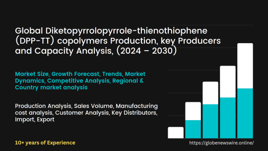
Who are the top ten producers of Diketopyrrolopyrrole-thienothiophene (DPP-TT) copolymers globally
Ossila Ltd. (United Kingdom)
Ossila is among the most recognized suppliers of organic semiconductors in Europe, providing high-purity DPP-TT copolymers primarily for research applications. Their production focuses on PDPP2T-TT-OD and similar derivatives, with tight control over molecular weight and purity. Ossila’s Diketopyrrolopyrrole-thienothiophene (DPP-TT) copolymers production is primarily batch-based, serving universities, research institutions, and materials testing labs. While their production capacity is modest, Ossila remains a key player in supplying consistent materials for academic and prototype development.
2. Merck KGaA (Germany)
Merck, operating through its Sigma-Aldrich brand, supplies a wide array of functional organic materials, including DPP-TT copolymers. As a large multinational chemical group, Merck leverages advanced synthesis technologies to maintain scalability and purity in DPP-TT copolymers production. Their target segments include OPV developers, transistor researchers, and flexible electronics innovators. Merck’s production capacity is among the largest in the research-grade category, serving both academia and pilot-level industrial applications globally.
3. Polyera Corporation (United States)
Polyera has developed a robust portfolio of semiconducting materials for flexible and wearable electronics, with DPP-TT copolymers being central to its offering. The company’s DPP-TT copolymers production is integrated into its flexible device prototyping operations, enabling end-to-end material and device innovation. Polyera’s DPP-TT materials are optimized for high mobility and environmental stability, making them suitable for organic TFTs, logic circuits, and e-skins. Their market focus includes next-generation consumer electronics and healthcare sensors.
4. Sumitomo Chemical Co., Ltd. (Japan)
As a global leader in materials science, Sumitomo Chemical has established itself as a leading producer of organic semiconductors. Their advanced R&D capabilities allow them to synthesize and scale DPP-TT copolymers production for both development and commercial use. Sumitomo targets industrial clients involved in OLED displays, OPVs, and printed electronics. Its DPP-TT product lines are designed for high efficiency and are compatible with roll-to-roll processing. With an eye on commercial-scale deployment, Sumitomo’s production capacity stands out in Asia.
5. Solarmer Energy Inc. (United States)
Solarmer Energy focuses on commercializing organic photovoltaics and has invested heavily in developing DPP-TT-based polymers for lightweight and flexible solar cells. The company’s DPP-TT copolymers are optimized for high absorption and charge mobility, key traits for energy harvesting applications. Solarmer’s Diketopyrrolopyrrole-thienothiophene (DPP-TT) copolymers production capacity is tailored to pilot manufacturing and device integration. Their customer base spans green building materials, off-grid electronics, and defense-related energy solutions.
6.Heraeus Holding GmbH (Germany)
Heraeus has diversified into advanced materials and solution-processable semiconductors, offering DPP-TT copolymers for printed and flexible electronics. Their DPP-TT copolymers production serves high-end applications like smart packaging, medical diagnostics, and intelligent sensors. Heraeus excels in converting functional materials into printable inks, making them suitable for industrial-scale printed circuit applications. Their production capacity is configured to meet demands from pilot programs and low-to-mid scale manufacturing.
7. Cambridge Display Technology Ltd. (United Kingdom)
Cambridge Display Technology (CDT), a subsidiary of Sumitomo Chemical, is a pioneer in organic semiconductors. While CDT does not sell materials directly, its innovations in DPP-TT copolymers have significantly influenced device performance in polymer-based electronics. CDT licenses its technology and provides custom material solutions, enabling companies in OLED and OFET industries to incorporate advanced DPP-TT-based materials. Their production strategy centers on high-purity synthesis and intellectual property development.
8. Brilliant Matters (Canada)
Brilliant Matters is a fast-growing Canadian startup specializing in the scalable synthesis of conjugated polymers. The company provides research and pilot-scale quantities of DPP-TT copolymers with high reproducibility. Their target markets include academic labs and device prototyping companies in North America and Europe. Brilliant Matters' production philosophy emphasizes sustainability and green chemistry. Their Diketopyrrolopyrrole-thienothiophene (DPP-TT) copolymers production capacity is expected to expand as demand grows from OPV and wearable device developers.
9. Rieke Metals Inc. (United States)
Rieke Metals produces a wide range of custom and catalog organic semiconductors, including DPP-TT copolymers for optoelectronic research. The company caters to research labs needing precise polymer structures and consistent molecular weights. Rieke’s DPP-TT copolymers production is centered on gram-to-kilogram scale synthesis, and they provide custom derivatives for specific electronic needs. Their main customer base includes academic institutions, research consortia, and biotech startups integrating organic sensors.
10. Raynergy Tek Inc. (Taiwan)
Raynergy Tek is a key Asian player in the organic materials sector, offering various polymer donors and acceptors for OPV applications. The company has successfully developed DPP-TT copolymers for solar and transistor markets. Its DPP-TT copolymers production benefits from close integration with roll-to-roll coating partners and device fabricators. Raynergy Tek’s production capacity is aimed at scaling new-generation organic electronics, particularly in the Asia-Pacific region, and they serve module makers and academic labs alike.
Summary and Outlook
The production landscape for Diketopyrrolopyrrole-thienothiophene (DPP-TT) copolymers remains relatively specialized but is steadily expanding as commercial applications grow. The top producers highlighted above collectively represent the most advanced and scalable DPP-TT copolymers production capacity available globally. While most current production remains in research and pilot-scale quantities, the increasing focus on flexible, low-cost electronics and green energy will likely catalyze further capacity expansion.
Most producers continue to focus on sectors such as organic solar cells, printed sensors, flexible displays, and bioelectronics. As demand for low-energy, flexible electronic materials increases, DPP-TT copolymers are well-positioned to become one of the foundational building blocks in next-generation electronic systems.
Top five largest Diketopyrrolopyrrole-thienothiophene (DPP-TT) copolymers producing countries globally
1. United States
The United States is one of the largest producers of Diketopyrrolopyrrole-thienothiophene (DPP-TT) copolymers globally. The country’s production is driven by a combination of academic innovation and startup ecosystems. Companies such as Polyera Corporation, Rieke Metals, and Solarmer Energy have developed significant DPP-TT copolymers production capabilities, supplying materials for organic field-effect transistors and flexible solar devices. In addition, research institutions and national laboratories actively support polymer development and scalability. The United States maintains a robust production capacity across lab-scale and pilot-scale levels, making it a global leader in both technology and output.
2. Germany
Germany has a strong foundation in chemical manufacturing and materials science, making it a key contributor to global DPP-TT copolymers production. Merck KGaA and Heraeus are central to the country’s output, producing high-purity DPP-TT copolymers for electronics, sensors, and OPV applications. Germany’s production capacity is also supported by advanced process engineering, regulatory infrastructure, and its status as a hub for printed electronics. German producers emphasize quality, repeatability, and industrial application-readiness, placing the country among the top in global capacity and commercial viability.
3. Japan
Japan is renowned for its deep expertise in organic electronics and polymer materials. Sumitomo Chemical plays a leading role in Japan’s DPP-TT copolymers production, focusing on large-scale synthesis and device integration. Japan’s industry is highly vertically integrated, allowing smooth transitions from lab-scale production to industrial-scale deployment. The country’s DPP-TT production supports sectors such as organic displays, solar films, and high-speed organic transistors. Japan’s production capacity is among the most sophisticated, serving both domestic electronics giants and global clients.
4. United Kingdom
The United Kingdom has developed into a significant player in Diketopyrrolopyrrole-thienothiophene (DPP-TT) copolymers production, primarily through advanced academic-industrial collaboration. Ossila Ltd. and Cambridge Display Technology are two key organizations contributing to the country’s output. The UK’s production focuses more on research and prototyping, serving universities and early-stage device developers. While not large in volume, the UK's DPP-TT production capacity is high in technical precision and research value, enabling global material testing and device trials.
5. Taiwan
Taiwan has rapidly advanced in organic semiconductor manufacturing, supported by its strong electronics supply chain. Raynergy Tek is one of the country’s leading DPP-TT copolymers producers, supplying materials for flexible solar cells and transistor applications. Taiwan’s production capacity is designed for both R&D and emerging commercial deployments. Its strategic focus is on materials that are compatible with roll-to-roll and inkjet printing techniques, helping to reduce production costs and enable scalability.
Diketopyrrolopyrrole-thienothiophene (DPP-TT) copolymers production trends
Diketopyrrolopyrrole-thienothiophene (DPP-TT) copolymers have garnered significant attention in the field of organic electronics due to their exceptional charge-carrier mobility, thermal stability, and tunable optoelectronic properties. These characteristics make them ideal candidates for applications in organic field-effect transistors (OFETs), organic photovoltaics (OPVs), and flexible electronic devices. Recent trends in DPP-TT copolymers production reflect advancements in molecular design, processing techniques, and application development.
Advancements in Molecular Design
The molecular architecture of DPP-TT copolymers has been a focal point of research, aiming to enhance their electronic properties. Incorporating donor–acceptor (D–A) structures within the polymer backbone has proven effective in reducing the bandgap, thereby extending light absorption into the near-infrared region. Modifications such as introducing different aromatic linkers, including thiophene, thienothiophene, and bithiophene, have been explored to fine-tune the electronic energy levels and improve charge transport. These structural variations influence the morphology and crystallinity of the resulting polymers, which are critical factors in determining device performance.
Processing Techniques and Scalability
The scalability of DPP-TT copolymers production has been addressed through the development of solution-processable methods compatible with large-area fabrication. Techniques such as doctor blading, inkjet printing, and spray coating have been investigated for their ability to produce uniform thin films with controlled thickness and morphology. These methods are conducive to roll-to-roll manufacturing, which is essential for the commercial viability of organic electronic devices. Moreover, the use of eco-friendly solvents and the optimization of processing parameters have been emphasized to align with sustainable manufacturing practices.
Application Development and Market Trends
The application spectrum of DPP-TT copolymers has expanded beyond traditional OFETs and OPVs. Their integration into stretchable and wearable electronics has been facilitated by blending with elastomeric materials, resulting in triblock copolymers that maintain high charge mobility under mechanical deformation. Such developments are pivotal for the advancement of flexible sensors, electronic skins, and other next-generation devices. Additionally, the compatibility of DPP-TT copolymers with all-polymer photodetectors has been explored, highlighting their potential in optoelectronic applications requiring mechanical flexibility and environmental stability.
Global Production Landscape
The production of DPP-TT copolymers is concentrated in countries with robust research infrastructures and advanced chemical manufacturing capabilities. The United States, Germany, Japan, the United Kingdom, and Taiwan are among the leading producers, with companies and research institutions focusing on both fundamental studies and commercial applications. Collaborations between academia and industry have been instrumental in transitioning from laboratory-scale synthesis to pilot-scale production, addressing challenges related to material consistency, scalability, and cost-effectiveness.
#Diketopyrrolopyrrole-thienothiophene (DPP-TT) copolymers price#production#Diketopyrrolopyrrole-thienothiophene (DPP-TT) copolymers import-export#key application
1 note
·
View note