#Verilog Systems Training
Explore tagged Tumblr posts
Visit Tumblr Blog
Explore Tumblr blogs with no restrictions, modern design and the best experience.
Last Seen Tumblr Blogs


Fun Fact
Tumblr Inc. is funded by 13 investors.
Text
Paving the Path to VLSI Success: A Deep Dive into Learning Opportunities
The Rising Demand for VLSI Professionals
In today’s technology-driven world, the demand for skilled professionals in the field of Very-Large-Scale Integration (VLSI) continues to surge. VLSI technology forms the foundation of most modern electronic devices, from smartphones to satellites. As integrated circuits become more complex, the need for engineers who can design, test, and improve these systems grows. Engineering students and electronics graduates looking to future-proof their careers are increasingly drawn to VLSI as a specialization. Companies in India and around the world are on the lookout for talent equipped with practical VLSI skills, making this an attractive career path. Given this scenario, educational institutions and private training centers have stepped up to provide in-depth programs designed to meet industry needs. Aspiring engineers now have a variety of options to choose from when selecting the right program to build their foundation in VLSI technology.
Importance of Industry-Relevant Training in VLSI
While a formal degree in electronics or electrical engineering provides the basics, industry-relevant training in VLSI is critical for practical success. This is because VLSI is highly application-based, demanding a strong understanding of design tools, programming languages, and testing methodologies. Hands-on experience with CAD tools, simulation software, and real-time projects can make all the difference. As a result, the choice of a training institute becomes an important factor. Students looking to enter this domain often search for the top vlsi institutes in hyderabad, as Hyderabad is a major technology hub with several reputed centers offering quality training. These institutes focus on practical exposure, experienced faculty, and placement support, all of which are key to student success. With proper guidance and the right learning environment, students can gain the skills required to thrive in this competitive field.
Choosing the Right VLSI Course
Selecting the right VLSI course is essential for aligning one's career goals with market expectations. The ideal course not only covers theoretical knowledge but also emphasizes real-world application. Curriculum components typically include digital design, CMOS technology, Verilog/VHDL, ASIC design, and FPGA implementation. Additionally, courses offering modules on SystemVerilog, UVM, and embedded systems are becoming increasingly popular. When evaluating course offerings, many prospective students explore vlsi courses in hyderabad to find a comprehensive program that covers both front-end and back-end design processes. It is important for learners to also consider the duration, mode of delivery (online/offline), and availability of project work. A structured course with industry-certified trainers and access to advanced lab setups can provide a valuable edge in this field. This clarity helps learners not only gain knowledge but also build a strong portfolio that can appeal to future employers.
Placement Support and Career Opportunities
One of the biggest advantages of enrolling in a reputed VLSI training program is the access to placement support. Leading institutes often have tie-ups with semiconductor companies, startups, and multinational corporations looking for trained professionals. Career opportunities in VLSI are vast, ranging from physical design engineers to verification specialists and DFT engineers. With the growth of IoT, AI, and 5G technologies, VLSI engineers are finding exciting roles in hardware development teams across domains. Institutes that focus on industry connections, mock interviews, resume building, and internships significantly boost a student’s employability. Moreover, alumni networks and mentorship programs help learners stay updated on trends and job openings. A combination of technical skills and soft skills training can greatly improve the likelihood of landing a dream role. As the semiconductor industry continues to grow, so too does the demand for qualified, hands-on VLSI professionals.
Conclusion: Begin Your VLSI Journey with Confidence
Choosing the right institute and course is the first step toward a successful VLSI career. From understanding the fundamentals to mastering design and verification tools, a structured training program can be a game changer. Whether you're a fresh graduate or a working professional looking to switch domains, VLSI offers a dynamic and rewarding path. Hyderabad, as a tech hub, continues to provide ample opportunities for learning and growth in this field. Institutes that combine practical training, expert mentorship, and placement assistance can help bridge the gap between education and employment. If you're looking to start or elevate your career in this domain, takshila-vlsi.com is a reliable place to begin your journey.
0 notes
Text
System Verilog Training Institutes In Hyderabad | Takshila-vlsi.com
At Takshila-vlsi.com, the premier institute in Hyderabad, you can revolutionise your career by receiving the highest quality System Verilog training. Begin your enrolment today and achieve success in VLSI!
system verilog training institutes in hyderabad
0 notes
Text
Mastering VLSI Design: The Path to a Promising Career in Semiconductor Industry
The Rising Demand for VLSI Professionals
The semiconductor industry is experiencing a dramatic shift, powered by the growing demand for smaller, faster, and more efficient chips in everything from smartphones to electric vehicles. Very-Large-Scale Integration (VLSI) design plays a critical role in this transformation, enabling the integration of millions of transistors onto a single chip. As technology continues to evolve, the need for skilled VLSI engineers is expanding at an unprecedented rate. This demand has opened up a world of opportunities for those interested in chip design and semiconductor engineering. Companies worldwide are investing in VLSI talent to maintain a competitive edge, making this an ideal time for students and professionals to build a career in the field. Whether it’s designing system-on-chip (SoC) solutions or optimizing embedded systems, VLSI experts are becoming increasingly vital to the tech ecosystem.
Understanding the Fundamentals of VLSI Design
VLSI design involves the process of creating integrated circuits by combining thousands or even millions of transistors into a single chip. This complex engineering task requires a deep understanding of electronic circuit design, semiconductor physics, and design tools like Verilog, SystemVerilog, and VHDL. The curriculum in most vlsi training institutes includes modules on front-end and back-end design, logic synthesis, timing analysis, and verification methods. The end goal is to produce high-performance chips that are also power-efficient and cost-effective. VLSI engineers must possess strong analytical skills, a deep interest in electronics, and a passion for solving real-world problems. As technology nodes continue to shrink from 7nm to 3nm and beyond, the challenges in VLSI design grow more complex—demanding not just theoretical knowledge but also hands-on experience in state-of-the-art tools and practices.
Exploring Career Opportunities in VLSI
A career in VLSI is not only intellectually rewarding but also financially lucrative. From design engineers to physical design experts and verification engineers, the job roles in this domain are diverse and highly specialized. Each position plays a crucial part in bringing a semiconductor product from concept to fabrication. What makes VLSI especially appealing is the steady demand from both startups and tech giants involved in AI, IoT, and 5G innovation. Particularly in India, the ecosystem around semiconductor design is growing, creating an urgent need for competent professionals. The rise of online vlsi training institutes in bangalore has made it easier for aspiring engineers to access high-quality education and training without geographical constraints. With remote learning tools, recorded sessions, and access to simulators, these platforms are revolutionizing how VLSI education is delivered, allowing learners to gain industry-relevant skills from the comfort of their homes.
Key Skills and Tools Every VLSI Engineer Should Learn
To thrive in the VLSI domain, aspiring engineers must master a combination of technical skills and practical tools. On the technical side, knowledge of digital electronics, CMOS design principles, and signal integrity is foundational. On the software front, proficiency in EDA (Electronic Design Automation) tools like Cadence, Synopsys, and Mentor Graphics is a must. Additionally, scripting languages such as Perl, Python, and Tcl are used to automate repetitive design and verification tasks. Industry expectations are high, and candidates are often evaluated not just for their academic background but for their problem-solving ability, project experience, and understanding of real-time design constraints. VLSI is a continuously evolving field, and engineers must commit to lifelong learning to stay ahead. Regularly updating one’s knowledge through webinars, certifications, and self-guided projects is crucial to success in this fast-paced industry.
Choosing the Right Institute for VLSI Training
Given the complexity and depth of the VLSI field, selecting the right training institute becomes a vital step in one’s professional journey. The ideal institute offers a blend of theoretical instruction and practical exposure, mentored by industry veterans. It should provide access to real-world design tools, capstone projects, and placement support. Moreover, flexibility in learning schedules and a structured curriculum aligned with industry requirements can make a significant difference. One such platform that offers all these features is takshila-vlsi.com, a trusted name in the VLSI education space. With a commitment to quality and innovation, Takshila VLSI equips learners with the skills needed to succeed in the semiconductor industry, bridging the gap between academic knowledge and practical application.
0 notes
Text
AlphaEvolve Coding Agent using LLM Algorithmic Innovation

AlphaEvolve
Large language models drive AlphaEvolve, a powerful coding agent that discovers and optimises difficult algorithms. It solves both complex and simple mathematical and computational issues.
AlphaEvolve combines automated assessors' rigour with LLMs' creativity. This combination lets it validate solutions and impartially assess their quality and correctness. AlphaEvolve uses evolution to refine its best ideas. It coordinates an autonomous pipeline that queries LLMs and calculates to develop algorithms for user-specified goals. An evolutionary method improves automated evaluation metrics scores by building programs.
Human users define the goal, set assessment requirements, and provide an initial solution or code skeleton. The user must provide a way, usually a function, to automatically evaluate produced solutions by mapping them to scalar metrics to be maximised. AlphaEvolve lets users annotate code blocks in a codebase that the system will build. As a skeleton, the remaining code lets you evaluate the developed parts. Though simple, the initial program must be complete.
AlphaEvolve can evolve a search algorithm, the solution, or a function that creates the solution. These methods may help depending on the situation.
AlphaEvolve's key components are:
AlphaEvolve uses cutting-edge LLMs like Gemini 2.0 Flash and Gemini 2.0 Pro. Gemini Pro offers deep and insightful suggestions, while Gemini Flash's efficiency maximises the exploration of many topics. This ensemble technique balances throughput and solution quality. The major job of LLMs is to assess present solutions and recommend improvements. AlphaEvolve's performance is improved with powerful LLMs despite being model-agnostic. LLMs either generate whole code blocks for brief or completely changed code or diff-style code adjustments for focused updates.
Prompt Sample:
This section pulls programs from the Program database to build LLM prompts. Equations, code samples, relevant literature, human-written directions, stochastic formatting, and displayed evaluation results can enhance prompts. Another method is meta-prompt evolution, where the LLM suggests prompts.
Pool of Evaluators
This runs and evaluates proposed programs using user-provided automatic evaluation metrics. These measures assess solution quality objectively. AlphaEvolve may evaluate answers on progressively complicated scenarios in cascades to quickly eliminate less promising examples. It also provides LLM-generated feedback on desirable features that measurements cannot measure. Parallel evaluation speeds up the process. AlphaEvolve optimises multiple metrics. AlphaEvolve can only solve problems with machine-grade solutions, but its automated assessment prevents LLM hallucinations.
The program database stores created solutions and examination results. It uses an evolutionary algorithm inspired by island models and MAP-elites to manage the pool of solutions and choose models for future generations to balance exploration and exploitation.
Distributed Pipeline:
AlphaEvolve is an asynchronous computing pipeline developed in Python using asyncio. This pipeline with a controller, LLM samplers, and assessment nodes is tailored for throughput to produce and evaluate more ideas within a budget.
AlphaEvolve has excelled in several fields:
It improved hardware, data centres, and AI training across Google's computing ecosystem.
AlphaEvolve recovers 0.7% of Google's worldwide computer resources using its Borg cluster management system heuristic. This in-production solution's performance and human-readable code improve interpretability, debuggability, predictability, and deployment.
It suggested recreating a critical arithmetic circuit in Google's Tensor Processing Units (TPUs) in Verilog, removing unnecessary bits, and putting it into a future TPU. AlphaEvolve can aid with hardware design by suggesting improvements to popular hardware languages.
It sped up a fundamental kernel in Gemini's architecture by 23% and reduced training time by 1% by finding better ways to partition massive matrix multiplication operations, increasing AI performance and research. Thus, kernel optimisation engineering time was considerably reduced. This is the first time Gemini optimised its training technique with AlphaEvolve.
AlphaEvolve optimises low-level GPU operations to speed up Transformer FlashAttention kernel implementation by 32.5%. It can optimise compiler Intermediate Representations (IRs), indicating promise for incorporating AlphaEvolve into the compiler workflow or adding these optimisations to current compilers.
AlphaEvolve developed breakthrough gradient-based optimisation processes that led to novel matrix multiplication algorithms in mathematics and algorithm discovery. It enhanced Strassen's 1969 approach by multiplying 4x4 complex-valued matrices with 48 scalar multiplications. AlphaEvolve matched or outperformed best solutions for many matrix multiplication methods.
When applied to over 50 open mathematics problems, AlphaEvolve enhanced best-known solutions in 20% and rediscovered state-of-the-art solutions in 75%. It improved the kissing number problem by finding a configuration that set a new lower bound in 11 dimensions. Additionally, it improved bounds on packing difficulties, Erdős's minimum overlap problem, uncertainty principles, and autocorrelation inequalities. These results were often achieved by AlphaEvolve using problem-specific heuristic search strategies.
AlphaEvolve outperforms FunSearch due to its capacity to evolve across codebases, support for many metrics, and use of frontier LLMs with rich context. It differs from evolutionary programming by automating evolution operator creation via LLMs. It improves artificial intelligence mathematics and science by superoptimizing code.
One limitation of AlphaEvolve is that it requires automated evaluation problems. Manual experimentation is not among its capabilities. LLM evaluation is possible but not the major focus.
AlphaEvolve should improve as LLMs code better. Google is exploring a wider access program and an Early Access Program for academics. AlphaEvolve's broad scope suggests game-changing uses in business, sustainability, medical development, and material research. Future phases include reducing AlphaEvolve's performance to base LLMs and maybe integrating natural-language feedback approaches.
#AlphaEvolve#googleAlphaEvolve#codingagent#AlphaEvolveCodingAgent#googleCodingAgent#largelanguagemodels#technology#technologynews#technews#news#govindhtech
0 notes
Text
VLSI Design and Technology Course at MVJCE: A Gateway to the Future of Electronics
MVJ College of Engineering (MVJCE), located in Whitefield, Bangalore, offers a specialized undergraduate program in Electronics Engineering with a focus on VLSI Design and Technology. This 4-year Bachelor of Engineering (B.E.) course is meticulously crafted to equip students with the knowledge and skills required to excel in the rapidly evolving field of Very-Large-Scale Integration (VLSI) and semiconductor technologies.
Program Overview
The VLSI Design and Technology program at MVJCE is affiliated with Visvesvaraya Technological University (VTU) and approved by the All India Council for Technical Education (AICTE). The curriculum is structured to provide a blend of theoretical knowledge and practical experience, ensuring that students are industry-ready upon graduation.
Key Features:
Industry-Oriented Curriculum: The program covers a comprehensive range of subjects, including Analog and Digital Electronics, Microelectronics, VLSI Design, Embedded Systems, and Hardware Description Languages (HDLs) such as Verilog and VHDL.
Hands-On Training: Students gain practical experience through well-equipped laboratories, industry visits, and internships, allowing them to apply theoretical concepts in real-world scenarios.
Elective Courses: The curriculum offers elective subjects that allow students to explore niche areas and advanced topics such as Advances in Image Processing, Reconfigurable Computing, Long Term Reliability of VLSI systems, SoC Design, System Verilog, and CMOS RF Circuit Design.
Honors and Minor Degrees: Students have the opportunity to earn an Honors or Minor degree by accumulating additional credits in specialized areas, aligning with the National Education Policy (NEP) guidelines.
Eligibility Criteria
For CET Quota Students:
Must have passed the Second Year of Pre-university or 12th standard or equivalent, with English as one of the subjects.
Must have secured an aggregate of at least 45% in Math and Physics, along with Chemistry / Biotechnology / Biology / Electronics / Computer Science.
Must have cleared the Karnataka Common Entrance Test (KCET). For Management Quota Students:
Must have passed the Second Year of Pre-university or 12th standard or equivalent, with English as one of the subjects and obtained an aggregate of at least 60% in Math and Physics, along with Chemistry / Biotechnology / Biology / Electronics / Computer Science.
Must have cleared any one of the Entrance Tests conducted by the Government of Karnataka or Government of India (KCET, COMEDK, JEE).
For Lateral Entry:
Must have passed the Diploma or equivalent examination as recognized by the University, and secured not less than 45% marks in the final year examination (fifth and sixth semesters), in the relevant branch of Engineering.
Must have cleared the Diploma Common Entrance Test (DCET) conducted by the Government of Karnataka
Career Opportunities
Graduates of the VLSI Design and Technology program at MVJCE are well-equipped to pursue careers in various sectors, including:
Semiconductor Industry: Roles in chip design, verification, and testing.
Embedded Systems: Designing and developing embedded systems for various applications.
Research and Development: Opportunities in exploring new technologies such as 3D ICs, neuromorphic computing, and quantum computing.
Academia: Pursuing higher studies and research in VLSI and related fields.
The program also emphasizes the development of soft skills, including communication and teamwork, enhancing employability in the global job market.
Conclusion
MVJCE's VLSI Design and Technology program offers a robust platform for students aspiring to make a mark in the electronics and semiconductor industries. With its comprehensive curriculum, hands-on training, and industry exposure, the program ensures that graduates are well-prepared to meet the challenges and opportunities in the dynamic field of VLSI design.
For more information or to apply, visit the MVJCE VLSI Design and Technology Program Page.
0 notes
Text
Master ASIC Design and Verification Training Today

In today’s fast-paced semiconductor industry, mastering ASIC (Application-Specific Integrated Circuit) design and verification is essential for engineers and professionals looking to advance their careers. With cutting-edge technology and increasing demand for customized chip designs, the need for skilled ASIC designers is greater than ever. If you are eager to enhance your expertise, ASIC Design and Verification Training is the perfect opportunity to gain in-depth knowledge and practical skills.
Why Choose ASIC Design and Verification Training?
ASIC design is a complex yet rewarding field that requires a deep understanding of digital circuits, system architecture, and verification methodologies. This training equips you with:
Fundamental and Advanced ASIC Design Concepts – Learn the principles of ASIC development, from design to implementation.
Verification Techniques – Master simulation-based verification, formal verification, and functional testing.
Industry-Standard Tools – Get hands-on experience with tools like Verilog, VHDL, SystemVerilog, and UVM.
Practical Projects and Case Studies – Work on real-world projects to strengthen your problem-solving abilities.
Expert Guidance – Learn from industry professionals with years of experience in ASIC design and verification.
Who Should Enroll?
This training is ideal for:
Engineering students and graduates looking to specialize in VLSI and ASIC design.
Working professionals aiming to upskill in semiconductor design.
Anyone passionate about learning digital design and verification methodologies.
Career Benefits of ASIC Design and Verification Online Training
With expertise in ASIC design and verification, you can unlock various career opportunities in semiconductor and electronics industries. Job roles include:
ASIC Design Engineer
Verification Engineer
FPGA Engineer
VLSI Design Engineer
Embedded Systems Engineer
Enroll Today and Advance Your Career!
Don’t miss the chance to boost your career in the high-demand field of ASIC design. Join ASIC Design and Verification Training today and gain the skills needed to thrive in the semiconductor industry. Start your journey towards success with expert-led training and hands-on experience.
At Multisoft Virtual Academy, we provide comprehensive training programs to help tech enthusiasts achieve professional excellence. Sign up now and take the next step in your career!
0 notes
Text
System Verilog Training Institutes In Bangalore | Takshila-vlsi.com
Unleash your full potential with Takshila-vlsi.com, the premier system verilog training institute in Bangalore. Achieve success in your professional life by acquiring practical experience.
system verilog training institutes in bangalore
0 notes
Text
System Verilog for Functional Verification – Inskill Courses
In today’s semiconductor industry, functional verification is crucial for ensuring reliable, high-quality VLSI design. Among the tools and methodologies available, SystemVerilog stands out as the most advanced and versatile hardware description and verification language. At Inskill, our SystemVerilog for Functional Verification course is tailored to help learners gain a competitive edge in this critical domain.

Why SystemVerilog for Functional Verification?
SystemVerilog combines the strengths of Verilog with modern features designed for robust verification processes. It enables seamless testbench development, functional coverage analysis, and efficient debugging of complex designs. Features like randomization techniques, procedural blocks, and interfaces make it the go-to language for designing testbenches in compliance with the UVM (Universal Verification Methodology).
Course Highlights
At Inskill, our course bridges the gap between academic learning and industry demands by offering:
Comprehensive training in SystemVerilog syntax and features.
Deep dives into testbench development, UVM, and functional coverage concepts.
Hands-on projects simulating real-world scenarios to build practical expertise.
Expert guidance from seasoned VLSI professionals.
Who Can Benefit?
Whether you are a fresh graduate, an aspiring VLSI engineer, or a working professional, this course will equip you with the knowledge and skills needed to advance your career. Learn how to develop robust verification environments and debug complex designs with confidence.
Why Choose Inskill?
Inskill is known for its industry-relevant courses that focus on advanced training, hands-on learning, and career-oriented skills. Our SystemVerilog for Functional Verification program ensures learners are industry-ready, making them valuable assets in the semiconductor industry.
Take the Next Step
Functional verification is a growing field with high demand for skilled engineers. Enroll in Inskill’s SystemVerilog for Functional Verification course today to master in-demand skills and accelerate your career in the semiconductor industry!
0 notes
Text
System Verilog Training Institutes In Bangalore | Takshila-vlsi.com
Unleash your full potential with Takshila-vlsi.com, the premier system verilog training institute in Bangalore. Achieve success in your professional life by acquiring practical experience.
system verilog training institutes in bangalore

0 notes
Text
NO.1 VLSI System Design in India
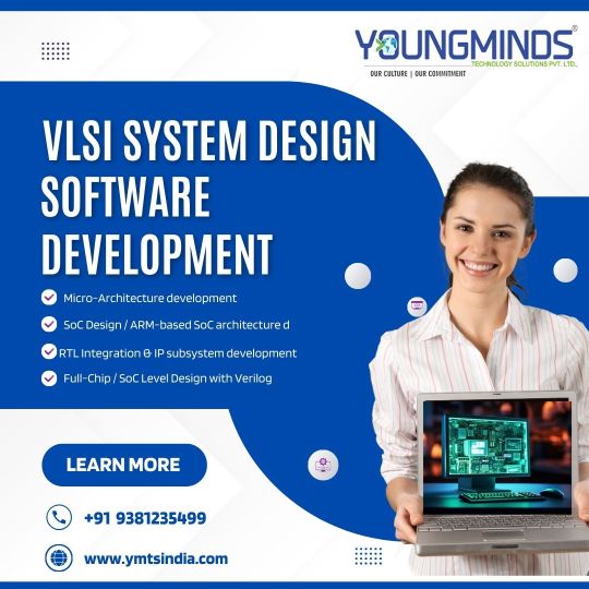
Welcome to Youngminds Technology Solutions, a leading VLSI System Design Software Development Agency in India. Our focus is on the development of the latest solutions that promote innovation and efficiency in the area of VLSI system design. Come with us as we are building the future of technology together.
Our VLSI design team has deep expertise in realizing product and software development for a wide range of application areas on cutting-edge technologies. YMTS team have wide set of skills across electronic chip design flow from specification to GDSII on latest node technologies, with special focus on RTL/FPGA Design, design verification and FPGA emulation.
VLSI SYSTEM DESIGN ASIC / FPGA Design Development
Design is not just what it looks like and feels like. Design is how it works.” You can hire us to build your custom website that fulfils your unique requirements. Unlike using a pre-built template for your site, a customized website is specifically created for you.
VLSI Services our Engineering team expertise in various stages of the design flow, Such as:
Micro-Architecture development for given specifications
SoC Design / ARM-based SoC architecture designs
RTL Integration & IP subsystem development
Full-Chip / SoC Level Design with Verilog, VHDL, System Verilog
Migration from FPGA to ASIC
Lint, CDC Checks and writing waivers
Integration of digital and analogue blocks (Like SERDES PMA + PCS or DDR + Phy etc.,)
Synthesis, STA Constraints for both ASIC and FPGA
Logic equivalency and formality checks
Hands-on experience on Various Industrial EDA tools
Optimization of Power, Area and timing trade off
FPGA Prototyping on Xilinx / Altera FPGA Boards
Optimization & Maintenance
We are here to help you understand the importance of web application maintenance. We provide several services which will enable your web application run error-free and smooth.
Our knowledge-based AI platform driven by automation and innovation. It enables our clients’ businesses to continuously reinvent system landscapes and achieve IT goals that align with business needs. By aligning IT with business value, we help clients push the envelope beyond cost and quality.
Training
YMTS provides training programs that help students / Engineers and customers get to productivity faster. All our training programs have been developed keeping in mind what it takes to accelerate skill development of today's R&D engineers and have been proven in-house with our own new hires as well as multiple customers.
As a top VLSI System Design Software Development Services, we are proud of the excellent services we offer. Our knowledge and dedication assure the best solutions for your VLSI requirements. Select us for the best performance in the VLSI system design. Visit More Information: https://ymtsindia.com/vlsi-system-design Meta Tags: VLSI System Design, VLSI System Management, VLSI Design Services, VLSI System Design Agency
0 notes
Text
High Performance FPGA Solutions

In today's rapidly evolving technological landscape, the demand for high-performance solutions is ever-increasing. Field-Programmable Gate Arrays (FPGAs) have emerged as versatile tools offering customizable hardware acceleration for a wide range of applications. Let's delve into the world of high performance FPGA solutions, exploring their key features, applications, challenges, recent advances, case studies, and future trends.
Introduction to High Performance FPGA Solutions
Definition of FPGA
Field-Programmable Gate Arrays (FPGAs) are semiconductor devices that contain an array of programmable logic blocks and configurable interconnects. Unlike Application-Specific Integrated Circuits (ASICs), FPGAs can be programmed and reprogrammed after manufacturing, allowing for flexibility and customization.
Importance of High Performance in FPGA Solutions
High performance is crucial in FPGA solutions to meet the demanding requirements of modern applications such as real-time data processing, artificial intelligence, and high-frequency trading. Achieving optimal speed, throughput, and efficiency is paramount for maximizing the effectiveness of FPGA-based systems.
Key Features of High Performance FPGA Solutions
Speed and Throughput
High performance FPGA solutions are capable of executing complex algorithms and processing vast amounts of data with exceptional speed and efficiency. This enables real-time decision-making and rapid response to dynamic inputs.
Low Latency
Reducing latency is essential in applications where response time is critical, such as financial trading or telecommunications. High performance FPGAs minimize latency by optimizing data paths and processing pipelines.
Power Efficiency
Despite their high performance capabilities, FPGA solutions are designed to operate within strict power constraints. Advanced power management techniques ensure optimal performance while minimizing energy consumption, making FPGAs suitable for battery-powered or energy-efficient devices.
Flexibility and Reconfigurability
One of the key advantages of FPGAs is their inherent flexibility and reconfigurability. High performance FPGA solutions can adapt to changing requirements by reprogramming the hardware on-the-fly, eliminating the need for costly hardware upgrades or redesigns.
Applications of High Performance FPGA Solutions
Data Processing and Analytics
FPGAs excel in parallel processing tasks, making them ideal for accelerating data-intensive applications such as big data analytics, database management, and signal processing.
Artificial Intelligence and Machine Learning
The parallel processing architecture of FPGAs is well-suited for accelerating AI and ML workloads, including model training, inference, and optimization. FPGAs offer high throughput and low latency, enabling real-time AI applications in edge devices and data centers.
High-Frequency Trading
In the fast-paced world of financial markets, microseconds can make the difference between profit and loss. High performance FPGA solutions are used to execute complex trading algorithms with minimal latency, providing traders with a competitive edge.
Network Acceleration
FPGAs are deployed in network infrastructure to accelerate packet processing, routing, and security tasks. By offloading these functions to FPGA-based accelerators, network performance and scalability can be significantly improved.
Challenges in Designing High Performance FPGA Solutions
Complexity of Design
Designing high performance FPGA solutions requires expertise in hardware architecture, digital signal processing, and programming languages such as Verilog or VHDL. Optimizing performance while meeting timing and resource constraints can be challenging and time-consuming.
Optimization for Specific Tasks
FPGAs offer a high degree of customization, but optimizing performance for specific tasks requires in-depth knowledge of the application domain and hardware architecture. Balancing trade-offs between speed, resource utilization, and power consumption is essential for achieving optimal results.
Integration with Existing Systems
Integrating FPGA-based accelerators into existing hardware and software ecosystems can pose compatibility and interoperability challenges. Seamless integration requires robust communication protocols, drivers, and software interfaces.
Recent Advances in High Performance FPGA Solutions
Improved Architectures
Advancements in FPGA architecture, such as larger logic capacity, faster interconnects, and specialized processing units, have led to significant improvements in performance and efficiency.
Enhanced Programming Tools
New development tools and methodologies simplify the design process and improve productivity for FPGA developers. High-level synthesis (HLS) tools enable software engineers to leverage FPGA acceleration without requiring expertise in hardware design.
Integration with Other Technologies
FPGAs are increasingly being integrated with other technologies such as CPUs, GPUs, and ASICs to create heterogeneous computing platforms. This allows for efficient partitioning of tasks and optimization of performance across different hardware components.
Case Studies of Successful Implementation
Aerospace and Defense
High performance FPGA solutions are widely used in aerospace and defense applications for tasks such as radar signal processing, image recognition, and autonomous navigation. Their reliability, flexibility, and performance make them ideal for mission-critical systems.
Telecommunications
Telecommunications companies leverage high performance FPGA solutions to accelerate packet processing, network optimization, and protocol implementation. FPGAs enable faster data transfer rates, improved quality of service, and enhanced security in telecommunication networks.
Financial Services
In the highly competitive world of financial services, microseconds can translate into significant profits or losses. High performance FPGA solutions are deployed in algorithmic trading, risk management, and low-latency trading systems to gain a competitive edge in the market.
Future Trends in High Performance FPGA Solutions
Increased Integration with AI and ML
FPGAs will play a vital role in accelerating AI and ML workloads in the future, especially in edge computing environments where low latency and real-time processing are critical.
Expansion into Edge Computing
As the Internet of Things (IoT) continues to grow, there will be increasing demand for high performance computing at the edge of the network. FPGAs offer a compelling solution for edge computing applications due to their flexibility, efficiency, and low power consumption.
Growth in IoT Applications
FPGAs will find widespread adoption in IoT applications such as smart sensors, industrial automation, and autonomous vehicles. Their ability to handle diverse workloads, adapt to changing requirements, and integrate with sensor networks makes them an ideal choice for IoT deployments.
Conclusion
In conclusion, high performance FPGA solutions play a crucial role in driving innovation and accelerating the development of advanced technologies. With their unparalleled speed, flexibility, and efficiency, FPGAs enable a wide range of applications across industries such as aerospace, telecommunications, finance, and IoT. As technology continues to evolve, the demand for high performance FPGA solutions will only continue to grow, shaping the future of computing.
0 notes
Text
Takshila Institute of VLSI Technologies: Premier Verilog Training Institute in India
Verilog, a hardware description language (HDL), is fundamental in the design and development of digital systems, including microprocessors, FPGAs, and ASICs. Aspiring VLSI professionals often seek comprehensive training in Verilog to establish a strong foundation in digital design. Among the top choices for this specialized education is the Takshila Institute of VLSI Technologies, a renowned name in India offering exceptional Verilog training. Whether you're in Hyderabad or Bangalore, Takshila Institute stands out as a premier destination for mastering Verilog.
Takshila Institute’s Verilog training program is meticulously crafted to cater to students, fresh graduates, and working professionals. The course begins with the basics of digital design and progresses to advanced concepts, including combinational and sequential logic, testbenches, and synthesis. The curriculum emphasizes practical learning, allowing students to work on real-world design projects and understand how Verilog is used in creating functional digital systems.
One of the standout features of Takshila’s Verilog training is the hands-on experience it provides. Students gain expertise in writing, simulating, and debugging Verilog code using industry-standard tools such as Cadence and Synopsys. This practical exposure ensures learners can confidently apply their skills in professional environments. The program also includes modules on advanced design techniques, preparing students to tackle complex challenges in the VLSI domain.
The institute’s faculty comprises seasoned professionals with extensive experience in digital design and verification. Their personalized mentoring approach helps students grasp even the most challenging concepts with ease. Through interactive sessions and real-world examples, the faculty ensures that learners develop both theoretical knowledge and practical proficiency in Verilog.
Another advantage of choosing Takshila Institute is its strong placement support. The institute has established partnerships with leading semiconductor companies, enabling students to secure internships and full-time positions. Its dedicated placement team conducts mock interviews, resume-building workshops, and career counseling sessions, ensuring students are well-prepared for job opportunities in the VLSI sector.
Takshila Institute also caters to diverse learning needs by offering online verification training. This flexibility allows students from across India to access high-quality education without geographical constraints. Whether you are in Hyderabad, Bangalore, or any other part of the country, you can benefit from Takshila’s expert-led training programs.
In conclusion, the Takshila Institute of VLSI Technologies is a top-tier choice for those seeking Verilog training institutes in Bangalore. With its industry-aligned curriculum, experienced faculty, practical focus, and strong placement support, Takshila empowers students to excel in digital design and achieve their career goals in the VLSI industry.
0 notes
Text
Unlocking the Power of System Verilog Assertions with iSpec.ai
Introduction
Assertions play a pivotal role in hardware verification, both for dynamic (simulation based) verification and formal verification. These assertions, expressed in a specialized language, play a crucial role in ensuring the correctness and reliability of complex digital systems. However, crafting these assertions often requires a deep understanding of both the design under test and the intricacies of the assertion language itself. To simplify this process and empower engineers, Agnisys introduces iSpec.ai, a groundbreaking service that transforms natural English text into SystemVerilog Assertions (SVA) with precision and accuracy.
SystemVerilog Assertions: A Brief Overview
Before exploring iSpec.ai, let's first understand the significance of SystemVerilog Assertions in the verification industry. SVA is essential for engineers, enabling them to formally specify the intended behavior of their designs. By expressing properties and constraints concisely, SVA facilitates rigorous verification, detecting errors early in the design cycle and reducing the risk of costly rework and system failures during deployment. From simple temporal (time based) relationships to complex protocol specifications, SVA empowers engineers to articulate a wide range of design requirements with precision and clarity.
Approaching the Challenge: iSpec.ai
At Agnisys, our mission is to democratize the process of generating SVA, making it accessible to engineers of all backgrounds. We are marching towards our stated vision of automatically creating hardware design directly from specifications. With iSpec.ai, assertions can be easily created from natural language specification, bridging the gap between a natural language and hardware verification.
To achieve this ambitious goal, we leverage state-of-the-art Large Language Models (LLM), renowned for their exceptional ability to understand and map dependencies between input and output sequences. Harnessing the power of machine translation, iSpec.ai transforms English specifications into SVA. In developing iSpec.ai, we have adopted a hybrid approach, combining the principles of prompt engineering and fine-tuning LLMs for downstream tasks. This strategic fusion allows us to leverage the strengths of both methodologies, resulting in a service that excels in generating high-quality assertions tailored to the unique requirements of each user.
Understanding Large Language Models
At the heart of iSpec.ai lies the concept of (LLMs), representing a significant advancement in natural language processing. Built upon transformer architectures, these models possess the remarkable ability to understand and generate human-like text across various languages and domains. Central to the efficacy of LLMs is self-attention, a mechanism that enables the model to weigh the significance of different words in a sentence while generating its output. By attending to relevant context and dependencies within the input sequence, self-attention empowers LLMs to capture intricate patterns and semantics, facilitating accurate and contextually relevant text generation.

Fine-Tuning for Downstream Tasks
While pre-trained LLMs exhibit impressive capabilities out-of-the-box, fine-tuning allows us to tailor these models to specific downstream tasks, such as generating SVA. However, traditional fine-tuning approaches pose significant challenges, particularly in terms of memory and compute requirements.
Historically, Full Fine-Tuning has been the predominant method, involving the updating of all model weights during the fine-tuning process. This approach, while effective, demands substantial computational resources, making it impractical for training and deployment on consumer hardware.
Enter Parameter-Efficient Fine-Tuning (PEFT) techniques, a paradigm shift in model adaptation. One such technique, QLORA, has emerged as a game-changer, offering a scalable and memory-efficient solution for fine-tuning LLMs. Quantization reduces computational and memory costs by representing model parameters with lower-precision data types. By employing techniques such as 8-bit integer quantization, QLORA achieves significant compression without compromising model performance.
Complementing quantization, Low-Rank Adaptation (LORA) targets the reduction of trainable parameters by selecting lower-rank matrices within the model architecture. By freezing pretrained weights and adapting only a subset of parameters, LORA minimizes memory overhead while preserving the expressive power of the underlying LLM. In essence, QLORA enables efficient fine-tuning of LLMs on consumer hardware, overcoming the barriers associated with traditional approaches and unlocking new possibilities for downstream applications such as iSpec.ai.
Addressing Challenges and the Path Forward
Despite the remarkable capabilities of iSpec.ai in SVA generation, challenges persist, particularly regarding data availability for fine-tuning. Accessing high-quality training data for niche domains like hardware verification remains a hurdle. Recognizing this, iSpec.ai is a work in progress, continuously evolving with each iteration. We're committed to refining our dataset and improving accuracy through iterative development and collaboration with experts. By leveraging feedback and advancements in machine learning, we aim to overcome these challenges and push the boundaries of automated assertion synthesis. Join us in shaping the future of iSpec.ai. With your input, we'll continue to set new standards in assertion generation, empowering engineers with efficient and reliable verification processes.
Conclusion
With iSpec.ai, Agnisys redefines the landscape of SVA generation, offering engineers a transformative solution powered by state-of-the-art machine learning techniques. By seamlessly translating English specifications into precise assertions, iSpec.ai empowers engineers to accelerate the verification process and enhance the reliability of their designs. Leveraging the synergy of large language models, fine-tuning methodologies, and parameter-efficient techniques like QLORA, iSpec.ai stands as a testament to innovation in hardware verification, paving the way for a future where complex assertions are as accessible as plain English.
0 notes
Text
FPGA System Design Training - VLSI Guru
In the evolving world of digital design, FPGA System Design Training has become a cornerstone for engineers aspiring to excel in hardware design and embedded systems. VLSI Guru’s comprehensive FPGA System Design course equips you with the skills to design, develop, and implement FPGA-based systems using the latest industry tools and methodologies.

What is FPGA System Design?
FPGA (Field-Programmable Gate Array) System Design involves programming configurable logic blocks to create customized hardware solutions. FPGAs are widely used in applications like embedded systems, signal processing, and high-performance computing due to their flexibility, scalability, and speed.
Why Choose VLSI Guru for FPGA System Design Training?
1. Industry-Focused Curriculum
VLSI Guru’s training covers all essential aspects of FPGA System Design, including:
Basics of FPGA architecture and design flow.
Programming using VHDL and Verilog.
Advanced concepts like timing analysis, IP integration, and system optimization.
Hands-on experience with industry tools like Xilinx Vivado and Intel Quartus.
2. Hands-On Learning
Our training emphasizes practical exposure, allowing you to work on real-world FPGA projects such as:
Designing digital circuits.
Implementing communication protocols.
Developing hardware acceleration modules.
3. Expert Mentorship
Learn from experienced trainers with extensive industry expertise, ensuring you gain insights into real-world FPGA system design challenges and solutions.
4. Placement Assistance
VLSI Guru provides job-oriented training along with resume building, interview preparation, and placement support to help you secure roles in top hardware and semiconductor companies.
What Will You Learn?
Fundamentals of FPGA architecture and HDL programming.
Design, simulation, and implementation using Verilog/VHDL.
Prototyping on FPGA development boards.
Debugging and optimization techniques for FPGA-based systems.
Who Should Enroll?
This course is ideal for:
Engineering graduates in electronics, electrical, or related fields.
Freshers and professionals seeking a career in FPGA System Design.
Embedded system developers looking to enhance their hardware design skills.
Why FPGA System Design is in Demand
FPGAs are the backbone of modern electronics, powering innovations in telecommunications, automotive, IoT, and artificial intelligence. Skilled FPGA engineers are in high demand to meet the growing need for customized hardware solutions.
Join VLSI Guru Today
Get ahead in the competitive semiconductor industry with VLSI Guru’s FPGA System Design Training. Our hands-on approach, expert guidance, and career support ensure you are ready to tackle the challenges of FPGA-based system design.
Contact us now to learn more and take the first step toward an exciting career in FPGA design
0 notes
Text
Leading SystemVerilog and Verilog Training Institute in India
In today’s rapidly advancing semiconductor industry, knowledge of hardware description languages like Verilog and SystemVerilog is essential for anyone aiming to build a successful career in VLSI design and verification. Among the institutes offering quality training in this domain, Takshila Institute of VLSI Technologies has emerged as a top destination for professionals and students alike. Renowned for its comprehensive programs, it is widely recognized as one of the best System Verilog training institutes in Hyderabad and a trusted name for those seeking Verilog training institutes in Bangalore.
Takshila Institute of VLSI Technologies offers specialized training programs designed to provide in-depth understanding of Verilog and SystemVerilog, focusing on both RTL design and functional verification. The course begins with the fundamentals of digital design and gradually progresses to advanced topics such as constrained random verification, assertions, coverage analysis, and testbench architecture. This structured approach ensures that learners develop strong coding skills along with practical application in industry-level projects.
As one of the most sought-after SystemVerilog training institutes in Hyderabad, Takshila stands out for its hands-on teaching methodology. Students are trained using real-time projects and industry-standard EDA tools, enabling them to gain practical exposure that goes far beyond textbook learning. The institute's expert faculty, who bring years of industry experience, provide personalized guidance and mentorship throughout the course.
In addition, Takshila Institute is well known among learners seeking Verilog training institutes in Bangalore, thanks to its reputation for delivering high-quality online and hybrid learning options. Students from across the country enroll in its training programs due to the institute’s proven track record of successful placements, strong curriculum, and focus on career readiness.
What makes Takshila unique is its emphasis on both design and verification aspects. Whether you’re a beginner looking to learn Verilog from scratch or an experienced engineer aiming to master SystemVerilog for verification roles, the institute provides a pathway that aligns with individual career goals. Mock interviews, technical assessments, and resume preparation sessions are also part of the course to support students in their job search.
For those aspiring to become skilled VLSI engineers, Takshila Institute of VLSI Technologies offers the perfect blend of theoretical knowledge and practical experience. Recognized among the best SystemVerilog training institutes in Hyderabad and preferred by many searching for Verilog training institutes in Bangalore, Takshila is committed to empowering the next generation of semiconductor professionals with top-tier education and industry-aligned skills.
0 notes
Text
The Growing Demand for VLSI Training and Career Opportunities
The Importance of VLSI in the Semiconductor Industry
The field of Very Large Scale Integration (VLSI) has seen exponential growth in recent years, driven by the rapid advancements in semiconductor technology. With the ever-increasing demand for high-performance chips used in smartphones, computers, automotive electronics, and artificial intelligence, VLSI has become a crucial aspect of modern electronics. The need for skilled professionals in this domain is rising, leading to the emergence of specialized training institutes that equip students with the necessary knowledge and hands-on experience. Engineers with expertise in VLSI design and verification are highly sought after by global technology firms, making this an attractive career path for aspiring electronics engineers.
Skills and Knowledge Required for a Career in VLSI
A successful career in VLSI requires a deep understanding of digital design, analog and mixed-signal design, system-on-chip (SoC) architecture, and verification methodologies. Programming skills in hardware description languages like VHDL and Verilog are essential, along with expertise in Electronic Design Automation (EDA) tools. The learning curve for VLSI professionals is steep, as it involves both theoretical concepts and practical applications. Many engineers and students opt for professional training programs to bridge the gap between academic knowledge and industry expectations. In particular, enrolling in one of the top 10 VLSI training institutes can provide a strong foundation and industry exposure, helping individuals stay ahead in this competitive field.
The Role of Training Institutes in Shaping VLSI Professionals
VLSI training institutes play a significant role in preparing students for real-world industry challenges. These institutes offer comprehensive courses covering fundamental to advanced topics, ensuring that learners gain practical expertise. Training programs often include hands-on projects, industry-relevant case studies, and internship opportunities that enhance problem-solving abilities. Many training centers collaborate with semiconductor companies, providing students with valuable networking opportunities and job placements. Among the many options available, VLSI institutes in Bangalore are particularly renowned for their high-quality education and strong industry connections. As Bangalore is a hub for semiconductor companies, students trained here have a higher chance of securing rewarding job opportunities.
Career Opportunities and Future Scope in VLSI
With the rapid expansion of the semiconductor industry, the demand for skilled VLSI engineers continues to grow. Companies specializing in chip design, manufacturing, and embedded systems actively seek trained professionals who can contribute to the development of cutting-edge technologies. Career opportunities in this field are diverse, ranging from digital and analog design to verification and testing. Additionally, with the emergence of AI, IoT, and 5G, the scope for VLSI professionals is expanding further. Salaries in this domain are highly competitive, and individuals with specialized training can secure lucrative positions in leading global technology firms. Those who continue upgrading their skills and staying updated with industry trends will find themselves at the forefront of technological advancements.
Choosing the Right VLSI Training Institute
Selecting the right training institute is a crucial step in building a successful career in VLSI. Factors such as faculty expertise, course curriculum, industry collaborations, hands-on training, and placement assistance should be carefully evaluated before making a decision. Institutes that offer mentorship, real-time project exposure, and certification programs can significantly enhance a student’s career prospects. One such institute that has gained recognition for providing quality VLSI training is Takshila VLSI.com. By enrolling in a reputed training institute, aspiring VLSI professionals can equip themselves with the necessary skills and knowledge to excel in the semiconductor industry.
0 notes