#nanoneedle
Photo
Needles in Eyes
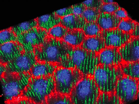
Sticking needles in your eyes might not be as bad as it seems. Any loss or damage to the inner layer of the cornea – the clear surface of the eye – can be permanent and lead to progressive sight loss. Corneal transplantation is the only available solution, and is invasive and limited, so researchers have developed a spiky new approach to restoring lost or damaged cells. They created a sheet of nanoneedles (green in the human cornea sample pictured) that can embed within the inner layer of cornea cells (red and blue), nestling down to the perfect depth. These needles can then directly deliver small strands of genetic material that interfere with a particular gene involved in keeping growth in check. With that silenced, cell growth increased. The nanoneedles can be integrated in contact lenses for long term drug delivery, restoring sight without sore eyes.
Written by Anthony Lewis
Image from work by Eleonora Maurizi and colleagues
Dentistry Centre Lab, University of Parma, Parma, Italy and Centre for Craniofacial and Regenerative Biology, King's College London, London, UK
Image originally published with a Creative Commons Attribution 4.0 International (CC BY 4.0)
Published in Advanced Science, October 2022
You can also follow BPoD on Instagram, Twitter and Facebook
#science#biomedicine#eyes#cornea#ophthalmology#sirna#nanoneedles#immunofluorescence#corneal transplant
9 notes
·
View notes
Text
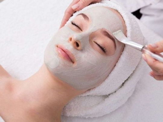
✨ ✨ Get ready to shine at The Sculpt Bar Aesthetics! ✨ ✨
Transform your skin with our cutting-edge medifacials and needling therapy. Say hello to radiant, glowing skin! Book your appointment now!

For appointments/enquiries:-
Call/WhatsApp: 9500605441/9159195441
Location : Chennai 📍Coimbatore 📍Bangalore
Read more - https://www.thesculptbaraesthetics.com/
#microneedling#nanoneedling#skintreatment#skincare#healthylifestyle#skincaretips#collagen#hydrafacial#glowingskin#cosmetology#doctors#dentist#beautician#womenentrepreneurs#glutathione#dermaplane#skincareroutine#bridaltreatment#mua#coimbatore#tirupur#erode#pollachi#coimbatoremakeupartist#tirupurmakeupartist#erodemakeupartist#salon
0 notes
Text
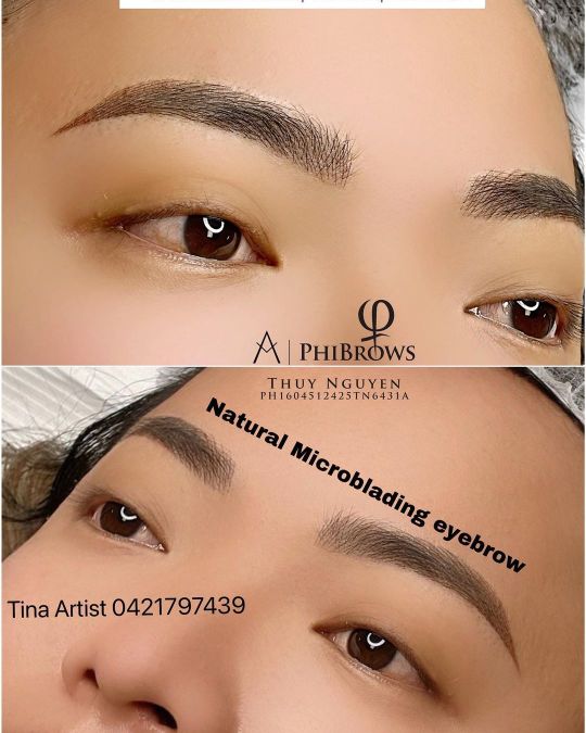
Nano Brows - Lux Brows and Lashes

Looking to elevate your brows? Discover Nano Brows - the next evolution in brow feathering. This breakthrough technique sculpts natural-looking brows with minimal discomfort thanks to nano needles. Experience beautiful, defined brows without the trauma of traditional microblading.
Experience feather-soft brows without the soreness. Take the first step towards the brows you've always wanted with Nano Brows. Book your consultation now!
#NanoBrows#Microblading#EyebrowTattoo#BrowEnhancement#PerfectBrows#BrowTransformation#FeatheredBrows#BrowGameStrong#BrowGoals#SemiPermanentBrows#EyebrowArt#BrowBeauty#NanoNeedling#BrowDesign#FlawlessBrows#BrowArtist#BrowSculpting#BrowPerfection#BrowInnovation#BrowTechnique
1 note
·
View note
Text
The Benefits of Nano Needling Facial for Acne: A Comprehensive Guide
What is Nano Needling?
Nano needling, also known as nano infusion, Nano Needling Facial for Acne is a non-invasive cosmetic procedure that uses a device equipped with microscopic needles to create tiny channels in the skin. Unlike traditional microneedling, which uses larger needles to penetrate deeper into the skin, nanoneedling targets the epidermis, the outermost layer. These nano-channels allow for the enhanced absorption of serums and active ingredients, promoting skin rejuvenation and addressing various skin concerns, including acne.
How Does Nano Needling Help with Acne?
Enhanced Product Absorption: The tiny nano-channels created during the procedure enhance the skin's ability to absorb topical treatments. This increased absorption means that acne-fighting ingredients, such as salicylic acid, benzoyl peroxide, and retinoids, can penetrate deeper and work more effectively.
Stimulates Collagen Production: Nano needling stimulates collagen and elastin production by creating controlled micro-injuries. This natural healing process helps to repair acne scars, smooth out uneven skin texture, and improve overall skin resilience.

Reduces Inflammation: The procedure helps to reduce inflammation and redness associated with active acne. By promoting healthier skin function and reducing bacterial load, nano needling can minimize the frequency and severity of breakouts.
Exfoliates Dead Skin Cells: Nano needling facilitates gentle exfoliation of the skin’s surface, removing dead skin cells that can clog pores and contribute to acne formation. This exfoliation process leaves the skin looking brighter and feeling smoother.
The Nano Needling Procedure
Consultation: A skincare professional will assess your skin condition and discuss your acne concerns, ensuring that nano needling is a suitable treatment for you.
Preparation: The skin is thoroughly cleansed to remove any makeup, oils, and impurities. A topical numbing cream may be applied to ensure comfort during the procedure.
Nano Needling: The nano needling device, which resembles a pen, is gently glided over the skin in a systematic manner. The microscopic needles create nano-channels, Laser Hair Removal Treatment Oakville allowing for optimal serum infusion. The entire process usually takes around 30 minutes to an hour, depending on the treatment area.
Post-Treatment Care: After the procedure, a soothing serum or mask may be applied to calm the skin. Patients are advised to avoid sun exposure and use gentle skincare products to aid the healing process.
Aftercare and Results
Following nano needling, it is crucial to adhere to a proper skincare regimen to maximize the benefits and ensure a smooth recovery. Here are some key aftercare tips:
Avoid Direct Sunlight: Use a broad-spectrum sunscreen with at least SPF 30 to protect the skin from harmful UV rays, which can exacerbate post-treatment sensitivity and pigmentation.
Gentle Skincare: Opt for mild, non-irritating cleansers and moisturizers. Avoid harsh exfoliants and active ingredients for at least a few days post-treatment.
Hydration: Keep the skin well-hydrated by using hydrating serums and moisturizers. Drinking plenty of water also helps to maintain skin hydration from within.
Patients can expect to see initial improvements in their skin’s texture and clarity within a week, with continued enhancement over the following weeks as collagen production ramps up. For optimal results, a series of treatments spaced a few weeks apart is often recommended.
0 notes
Text
A first-ever complete map for elastic strain engineering - Technology Org
New Post has been published on https://thedigitalinsider.com/a-first-ever-complete-map-for-elastic-strain-engineering-technology-org/
A first-ever complete map for elastic strain engineering - Technology Org
New research by a team of MIT engineers offers a guide for fine-tuning specific material properties.
Without a map, it can be impossible to know not only where you are but also where you’re going, and that’s especially true when it comes to materials’ properties.
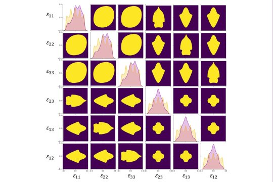
The “map,” or the phonon stability boundary, is a graphical representation that plots the stability regions of a crystal as a function of strain. This map helps scientists and engineers determine the conditions under which a material can exist in a particular phase and when it might fail or transition to another phase. By analyzing the phonon stability boundary, researchers can understand material properties at extreme conditions and design new materials with desired characteristics. Image courtesy of the researchers / MIT
For decades, scientists have understood that while bulk materials behave in certain ways, those rules can break down for materials at the micro- and nano-scales, and often in surprising ways. One of those surprises was the finding that, for some materials, applying even modest strains — a concept known as elastic strain engineering — on materials can dramatically improve certain properties, provided those strains stay elastic and do not relax away by plasticity, fracture, or phase transformations. Micro- and nano-scale materials are especially good at holding applied strains in the elastic form.
Precisely how to apply those elastic strains (or equivalently, residual stress) to achieve certain material properties, however, had been less clear — until recently.
Using a combination of first principles calculations and machine learning, a team of MIT researchers has developed the first-ever map of how to tune crystalline materials to produce specific thermal and electronic properties.
Led by Ju Li, the Battelle Energy Alliance Professor in Nuclear Engineering and professor of materials science and engineering, the team described a framework for understanding precisely how changing the elastic strains on a material can fine-tune properties like thermal and electrical conductivity. The work is described in an open-access paper published in PNAS.
“For the first time, by using machine learning, we’ve been able to delineate the complete six-dimensional boundary of ideal strength, which is the upper limit to elastic strain engineering, and create a map for these electronic and phononic properties,” Li says. “We can now use this approach to explore many other materials. Traditionally, people create new materials by changing the chemistry.”
“For example, with a ternary alloy, you can change the percentage of two elements, so you have two degrees of freedom,” he continues. “What we’ve shown is that diamond, with just one element, is equivalent to a six-component alloy, because you have six degrees of elastic strain freedom you can tune independently.”
Small strains, big material benefits
The paper builds on a foundation laid as far back as the 1980s, when researchers first discovered that the performance of semiconductor materials doubled when a small — just 1 percent — elastic strain was applied to the material.
While that discovery was quickly commercialized by the semiconductor industry and today is used to increase the performance of microchips in everything from laptops to cellphones, that level of strain is very small compared to what we can achieve now, says Subra Suresh, the Vannevar Bush Professor of Engineering Emeritus.
In a 2018 Science paper, Suresh, Dao, and colleagues demonstrated that 1 percent strain was just the tip of the iceberg.
As part of a 2018 study, Suresh and colleagues demonstrated for the first time that diamond nanoneedles could withstand elastic strains of as much as 9 percent and still return to their original state. Later on, several groups independently confirmed that microscale diamond can indeed elastically deform by approximately 7 percent in tension reversibly.
“Once we showed we could bend nanoscale diamonds and create strains on the order of 9 or 10 percent, the question was, what do you do with it,” Suresh says. “It turns out diamond is a very good semiconductor material … and one of our questions was, if we can mechanically strain diamond, can we reduce the band gap from 5.6 electron-volts to two or three? Or can we get it all the way down to zero, where it begins to conduct like a metal?”
To answer those questions, the team first turned to machine learning in an effort to get a more precise picture of exactly how strain altered material properties.
“Strain is a big space,” Li explains. “You can have tensile strain, you can have shear strain in multiple directions, so it’s a six-dimensional space, and the phonon band is three-dimensional, so in total there are nine tunable parameters. So, we’re using machine learning, for the first time, to create a complete map for navigating the electronic and phononic properties and identify the boundaries.”
Armed with that map, the team subsequently demonstrated how strain could be used to dramatically alter diamond’s semiconductor properties.
“Diamond is like the Mt. Everest of electronic materials,” Li says, “because it has very high thermal conductivity, very high dielectric breakdown strengths, a very big carrier mobility. What we have shown is we can controllably squish Mt. Everest down … so we show that by strain engineering you can either improve diamond’s thermal conductivity by a factor of two, or make it much worse by a factor of 20.”
New map, new applications
Going forward, the findings could be used to explore a host of exotic material properties, Li says, from dramatically reduced thermal conductivity to superconductivity.
“Experimentally, these properties are already accessible with nanoneedles and even microbridges,” he says. “And we have seen exotic properties, like reducing diamond’s (thermal conductivity) to only a few hundred watts per meter-Kelvin. Recently, people have shown that you can produce room-temperature superconductors with hydrides if you squeeze them to a few hundred gigapascals, so we have found all kinds of exotic behavior once we have the map.”
The results could also influence the design of next-generation computer chips capable of running much faster and cooler than today’s processors, as well as quantum sensors and communication devices. As the semiconductor manufacturing industry moves to denser and denser architectures, Suresh says the ability to tune a material’s thermal conductivity will be particularly important for heat dissipation.
While the paper could inform the design of future generations of microchips, Zhe Shi, a postdoc in Li’s lab and first author of the paper, says more work will be needed before those chips find their way into the average laptop or cellphone.
“We know that 1 percent strain can give you an order of magnitude increase in the clock speed of your CPU,” Shi says. “There are a lot of manufacturing and device problems that need to be solved in order for this to become realistic, but I think it’s definitely a great start. It’s an exciting beginning to what could lead to significant strides in technology.”
Written by Peter Reuell
Source: Massachusetts Institute of Technology
You can offer your link to a page which is relevant to the topic of this post.
#1980s#applications#approach#Behavior#cellphones#change#chemistry#Chemistry & materials science news#chips#communication#computer#computer chips#Computer modeling#cpu#crystal#crystalline#crystalline materials#Design#devices#diamonds#electron#electronic#Electronics#energy#engineering#engineers#factor#form#Foundation#framework
0 notes
Text
A first-ever complete map for elastic strain engineering
New Post has been published on https://sunalei.org/news/a-first-ever-complete-map-for-elastic-strain-engineering/
A first-ever complete map for elastic strain engineering

Without a map, it can be just about impossible to know not just where you are, but where you���re going, and that’s especially true when it comes to materials properties.
For decades, scientists have understood that while bulk materials behave in certain ways, those rules can break down for materials at the micro- and nano-scales, and often in surprising ways. One of those surprises was the finding that, for some materials, applying even modest strains — a concept known as elastic strain engineering — on materials can dramatically improve certain properties, provided those strains stay elastic and do not relax away by plasticity, fracture, or phase transformations. Micro- and nano-scale materials are especially good at holding applied strains in the elastic form.
Precisely how to apply those elastic strains (or equivalently, residual stress) to achieve certain material properties, however, had been less clear — until recently.
Using a combination of first principles calculations and machine learning, a team of MIT researchers has developed the first-ever map of how to tune crystalline materials to produce specific thermal and electronic properties.
Led by Ju Li, the Battelle Energy Alliance Professor in Nuclear Engineering and professor of materials science and engineering, the team described a framework for understanding precisely how changing the elastic strains on a material can fine-tune properties like thermal and electrical conductivity. The work is described in an open-access paper published in PNAS.
“For the first time, by using machine learning, we’ve been able to delineate the complete six-dimensional boundary of ideal strength, which is the upper limit to elastic strain engineering, and create a map for these electronic and phononic properties,” Li says. “We can now use this approach to explore many other materials. Traditionally, people create new materials by changing the chemistry.”
“For example, with a ternary alloy, you can change the percentage of two elements, so you have two degrees of freedom,” he continues. “What we’ve shown is that diamond, with just one element, is equivalent to a six-component alloy, because you have six degrees of elastic strain freedom you can tune independently.”
Small strains, big material benefits
The paper builds on a foundation laid as far back as the 1980s, when researchers first discovered that the performance of semiconductor materials doubled when a small — just 1 percent — elastic strain was applied to the material.
While that discovery was quickly commercialized by the semiconductor industry and today is used to increase the performance of microchips in everything from laptops to cellphones, that level of strain is very small compared to what we can achieve now, says Subra Suresh, the Vannevar Bush Professor of Engineering Emeritus.
In a 2018 Science paper, Suresh, Dao, and colleagues demonstrated that 1 percent strain was just the tip of the iceberg.
As part of a 2018 study, Suresh and colleagues demonstrated for the first time that diamond nanoneedles could withstand elastic strains of as much as 9 percent and still return to their original state. Later on, several groups independently confirmed that microscale diamond can indeed elastically deform by approximately 7 percent in tension reversibly.
“Once we showed we could bend nanoscale diamonds and create strains on the order of 9 or 10 percent, the question was, what do you do with it,” Suresh says. “It turns out diamond is a very good semiconductor material … and one of our questions was, if we can mechanically strain diamond, can we reduce the band gap from 5.6 electron-volts to two or three? Or can we get it all the way down to zero, where it begins to conduct like a metal?”
To answer those questions, the team first turned to machine learning in an effort to get a more precise picture of exactly how strain altered material properties.
“Strain is a big space,” Li explains. “You can have tensile strain, you can have shear strain in multiple directions, so it’s a six-dimensional space, and the phonon band is three-dimensional, so in total there are nine tunable parameters. So, we’re using machine learning, for the first time, to create a complete map for navigating the electronic and phononic properties and identify the boundaries.”
Armed with that map, the team subsequently demonstrated how strain could be used to dramatically alter diamond’s semiconductor properties.
“Diamond is like the Mt. Everest of electronic materials,” Li says, “because it has very high thermal conductivity, very high dielectric breakdown strengths, a very big carrier mobility. What we have shown is we can controllably squish Mt. Everest down … so we show that by strain engineering you can either improve diamond’s thermal conductivity by a factor of two, or make it much worse by a factor of 20.”
New map, new applications
Going forward, the findings could be used to explore a host of exotic material properties, Li says, from dramatically reduced thermal conductivity to superconductivity.
“Experimentally, these properties are already accessible with nanoneedles and even microbridges,” he says. “And we have seen exotic properties, like reducing diamond’s (thermal conductivity) to only a few hundred watts per meter-Kelvin. Recently, people have shown that you can produce room-temperature superconductors with hydrides if you squeeze them to a few hundred gigapascals, so we have found all kinds of exotic behavior once we have the map.”
The results could also influence the design of next-generation computer chips capable of running much faster and cooler than today’s processors, as well as quantum sensors and communication devices. As the semiconductor manufacturing industry moves to denser and denser architectures, Suresh says the ability to tune a material’s thermal conductivity will be particularly important for heat dissipation.
While the paper could inform the design of future generations of microchips, Zhe Shi, a postdoc in Li’s lab and first author of the paper, says more work will be needed before those chips find their way into the average laptop or cellphone.
“We know that 1 percent strain can give you an order of magnitude increase in the clock speed of your CPU,” Shi says. “There are a lot of manufacturing and device problems that need to be solved in order for this to become realistic, but I think it’s definitely a great start. It’s an exciting beginning to what could lead to significant strides in technology.”
This work was supported with funding from the Defense Threat Reduction Agency, an NSF Graduate Research Fellowship, the Nanyang Technological University School of Biological Sciences, the National Science Foundation (NSF), the MIT Vannevar Bush Professorship, and a Nanyang Technological University Distinguished University Professorship.
0 notes
Text

If you don't love how your skin looks or feels, we can help. We have a variety of product and treatment options available that can address pretty much any skin concern that you have. Let us help you create a treatment plan that'll work for you so you'll love your skin! 509-961-6555 #loveyourskin #dermaplaning #skincarestudio #skincare #esthetician #chemicalpeel #healthyskin #facialtreatment #vibrantskin #barebliss #nanoneedling #microneedling #skincareproducts #skinlightening #skincareprofessional #yakima #dermaplaningservice #skincareyakima #extractions #skincarespecialist #facialcupping #beauty #microdermabrasiontreatment #glowingskin #yakimaskincare #skincareroutine #facial #skinspecialist #microdermabrasion #radiantskin
0 notes
Text
Experience the ultimate hydration with our hydrating facial and hydrafacial treatment. Our skilled estheticians use advanced techniques and nourishing products to deeply moisturise and rejuvenate your skin. Achieve a glowing complexion and boost your confidence with our customised facial treatments.
Call us at (925)464-8088
#hydrating facial#hydrafacial treatment#Anti- Acne Treatment#Anti-Aging And lifting#Acne Scar Removal
0 notes
Text
Engineering Bifunctional Calcium Alendronate Gene-Delivery Nanoneedle for Synergistic Chemo/Immuno-Therapy Against HER2 Positive Ovarian Cancer
Ovarian cancer is the most lethal gynecological malignancy. Most patients are diagnosed at an advanced stage with widespread peritoneal dissemination and ascites. Bispecific T-cell engagers (BiTEs) have demonstrated impressive antitumor efficacy in hematological malignancies, but the clinical potency is limited by their short half-life, inconvenient continuous intravenous infusion, and severe toxicity at relevant therapeutic levels in solid tumors. To address these critical issues, the design... http://dlvr.it/Sl6mjt
0 notes
Text
NANO STROKES COURSE NEAR ME – iOWA iBROW iLASH ACADEMY & Spa
Are you eager to start your PMU career? Why not update your profile to mention nanoblading? Look no further than iOWA iBROW iLASH ACADEMY Spa for nano brow classes close to me. Near Iowa, we provide thorough nanostrokes training. You will learn various methods for using the nanoneedle for shading from our brow expert. We at iOWA iBROW iLASH ACADEMY Spa are here to assist you in adding a new page to your client list. We hope to assist our pupils in correcting their previous poor machine handling or ineffective strokes with our nano strokes training in Iowa. Both beginning and advanced students can enroll in one of our nano brow courses in Iowa. With our expert course, we are here to help you reach your career goals for permanent makeup, whether you want to build your clientele or start your brow career!
WHY CHOOSE OUR NANO BROW COURSES IN IOWA? WHAT CAN YOU EXPECT TO LEARN?
Students participating in the well-organized Nano strokes course near me in Iowa will study the procedures for nanoblading. Our students learn the craft of using nanoneedles to tattoo eyebrows in this course. Our nano brow courses close to Iowa educate our students how to fill the brows so that their customers can experience the appearance of fuller, thicker, and pigmented brows. If you’ve finished looking for nano strokes classes nearby in Iowa, get in touch with us to learn more about various Nanoblading hacks and techniques, such as
OMBRE BROWS
Our pupils will study the methods and fashion associated with ombre brows on the first day. Additionally, participants in the nano brow course in Iowa will learn about skin thickness, how thick and thin areas recover, and the step-by-step ombre shading procedure.
NANO BROW
The second day of the workshop will be devoted to growing brows that highlight your best facial features. Additionally, the students will learn about the purpose of each needle, the configuration of each needle, crucial eyebrow mapping, and eye and facial forms from our instructor. You will have the chance to watch the nano brow technique in action when you take one of our nano brow courses close to Iowa.
0 notes
Text
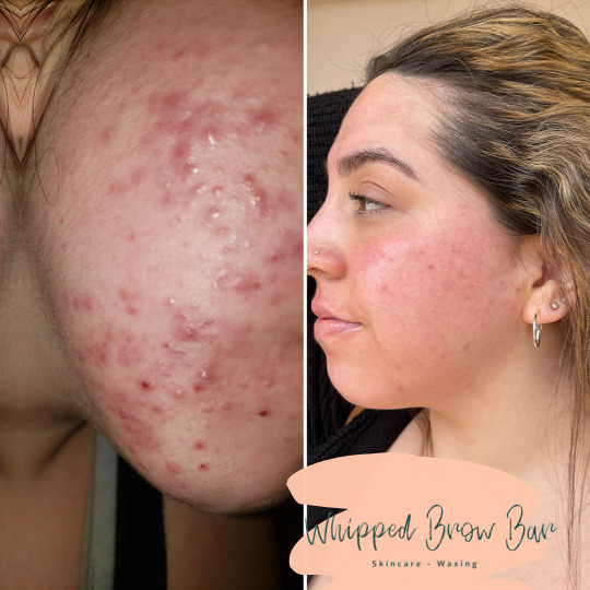
Try The Best Facial Treatment for Your Look This New Year.
These days, ladies are running behind in appearance. Everyone wants to look elegant, so how do you stand out in the crowd? You can try different facial and body treatments from different beauty salons, spas, and fitness centers but are they 100% skin-friendly, durable, and beauty-enhancing? You must be doubtful! So, why think about wasting money? When we are with you. This is Whipped Bro Bar, which offers you a reliable facial treatment in Albuquerque.
Whipped Bro Bar is currently an eminent facial treatment service in Albuquerque. Our make-up studio strives to unleash your beauty and persona with our unique art of professional makeover. Our facial skin care in Albuquerque is 100% natural, skin-friendly, and durable and adds a new texture, beauty, and style to your personality. For your best and most durable look, we have a widely dedicated team of make-up artists, and our products and procedures are fully safe for all skin types and at any age.
What is Facial Treatment and Its Importance?
You ask this! Well, facial treatment is simply a way to unwind and relax your skin pores. It is vital for your skin from time to time to maintain your facial glow, beauty, and healthy skin all at the same time. This beauty treatment may be a short or an hour-long session, depending on your skin condition. So, give your skin the best love and care with this multi-step treatment, which involves massage, exfoliation, CTM, and more. In short, cleaning, toning, and moisturizing.
Types Of Facial on Your Skin Conditions:
Derma Facial
It is a skin-resurfacing procedure in which the uppermost layer of your skin is shaved away to remove deeply ingrained dirt, oil, and vellus hair. And it is a minimally invasive procedure using a scalpel or a dermatome tool and a rotating brush to exfoliate the skin.
Nanoneedle Facial
Another minimally-invasive facial treatment to rejuvenate your skin. The procedure involves a nano-needling-based transdermal serum delivery system to stimulate your skin’s collagen production. Nano-needling tips are thinner than human hair. This design gives you a little prick but not severe pain, as you imagine.
Hydra Facial
HydraFacial is quite like a treatment called microdermabrasion. Under the treatment procedure, a mildly abrasive instrument is used to exfoliate your uppermost thicker and uneven skin. You can also call it hydradermabrasion, in which your normal exfoliation is paired with a typical hydrating serum.
Everyone wants to get smooth, bright, and youthful skin, and different types of facial treatments in Albuquerque are available for this reason. Facial skin care treatments can either last shorter or longer but definitely radiant your skin, so visit our website if you need the same service for your skin condition.
Call us at (505) 796-5599
Visit our website: https://whippedbrowbar.com/
#facial treatment Albuquerque#face skin care Albuquerque#oily face treatment Albuquerque#facial spa near me Albuquerque#back facial near me Albuquerque
0 notes
Photo
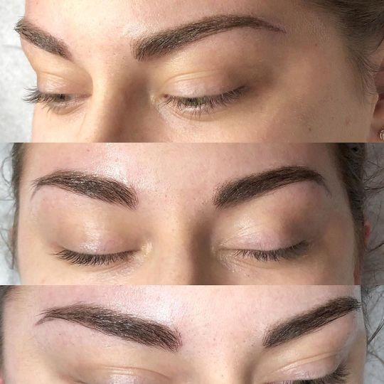
Eyebrow glow upppp, swipe for the before ! • • • • • #ink #inked #inkedmag #tattooedeyebrows #permanentmakeup #pmu #nashville #nashvilletattooartist #nashvillepmu #makeupartist #nashvillemakeupartist #permablend #nanoneedle #permananteyebrows (at Branded Tattoo Company) https://www.instagram.com/p/B7KPBbknSJD/?igshid=1a45k9bijq4wl
#ink#inked#inkedmag#tattooedeyebrows#permanentmakeup#pmu#nashville#nashvilletattooartist#nashvillepmu#makeupartist#nashvillemakeupartist#permablend#nanoneedle#permananteyebrows
12 notes
·
View notes
Text

🔹Rezenerate NanoFacial is the perfect marriage of science and beauty. Rezenerate elevates your facial by infusing nutrient-rich ingredients for the ultimate rejuvenation.
🔹Rezenerate works wonders on:
✔️Fine lines and other signs of aging skin
✔️Blemishes or other skin imperfections
✔️Malnourished skin
✔️Sunspots and age spots
✔️Oily or overly dry skin
✔️Uneven skin tone and texture
🔹Book your appointment now:
🔗https://skinpowerimage-spa.skincaretherapy.net/
📞281-979-8291; 713-819-6954
💌[email protected]
📍SkinPowerImage Spa & Wellness 8650 N Sam Houston Pkwy E #190 Humble, TX 77396, USA
#skinpowerimagespawellness#skincareroutine#skincaretips#skincareaddict#SkincareIsSelfcare#skincarecommunity#skincarelover#skincareislife#glowingskin#softskin#skintreatment#healthyskin#healthyskincare#hydratedskin#takecareofyourskin#rezenerate#rezeneratefacial#nanoneedling#nanoneedle#facialtreatment#facialtreatments#facialskincare#skincarethreads#skincaretreatments#skincaretrends#wrinklefree#finelinesandwrinkles#blemishfree#skincaretransformation
0 notes
Photo
🌹The best part of my job is combining my artist vision with the client’s vision and creating something so beautiful and classic for her! 🌺Gave her a brow lift and made her more youthful looking!���. . . . . . . #melbournetattooartist #lashtinting #perthbrows #dronfield #browtintandwax #semipermanentmakeupmanchester #melbournemicroblading #primecolor #nanoneedle #scattercrystals #browcare #facialservices #browdaddy #yycbrowtattoo #nzbrows #keratinlift #browsliverpool #lashesglue #melbournecosmetictattoo #luxuryfacials #powderbrowsmelbourne #microbladingeyebrowsartist #microbladingpen #microbladingexpert (at Springvale South, Victoria, Australia) https://www.instagram.com/p/CWppZRcPibG/?utm_medium=tumblr
#melbournetattooartist#lashtinting#perthbrows#dronfield#browtintandwax#semipermanentmakeupmanchester#melbournemicroblading#primecolor#nanoneedle#scattercrystals#browcare#facialservices#browdaddy#yycbrowtattoo#nzbrows#keratinlift#browsliverpool#lashesglue#melbournecosmetictattoo#luxuryfacials#powderbrowsmelbourne#microbladingeyebrowsartist#microbladingpen#microbladingexpert
0 notes
Text
A first-ever complete map for elastic strain engineering
New Post has been published on https://thedigitalinsider.com/a-first-ever-complete-map-for-elastic-strain-engineering/
A first-ever complete map for elastic strain engineering
Without a map, it can be just about impossible to know not just where you are, but where you’re going, and that’s especially true when it comes to materials properties.
For decades, scientists have understood that while bulk materials behave in certain ways, those rules can break down for materials at the micro- and nano-scales, and often in surprising ways. One of those surprises was the finding that, for some materials, applying even modest strains — a concept known as elastic strain engineering — on materials can dramatically improve certain properties, provided those strains stay elastic and do not relax away by plasticity, fracture, or phase transformations. Micro- and nano-scale materials are especially good at holding applied strains in the elastic form.
Precisely how to apply those elastic strains (or equivalently, residual stress) to achieve certain material properties, however, had been less clear — until recently.
Using a combination of first principles calculations and machine learning, a team of MIT researchers has developed the first-ever map of how to tune crystalline materials to produce specific thermal and electronic properties.
Led by Ju Li, the Battelle Energy Alliance Professor in Nuclear Engineering and professor of materials science and engineering, the team described a framework for understanding precisely how changing the elastic strains on a material can fine-tune properties like thermal and electrical conductivity. The work is described in an open-access paper published in PNAS.
“For the first time, by using machine learning, we’ve been able to delineate the complete six-dimensional boundary of ideal strength, which is the upper limit to elastic strain engineering, and create a map for these electronic and phononic properties,” Li says. “We can now use this approach to explore many other materials. Traditionally, people create new materials by changing the chemistry.”
“For example, with a ternary alloy, you can change the percentage of two elements, so you have two degrees of freedom,” he continues. “What we’ve shown is that diamond, with just one element, is equivalent to a six-component alloy, because you have six degrees of elastic strain freedom you can tune independently.”
Small strains, big material benefits
The paper builds on a foundation laid as far back as the 1980s, when researchers first discovered that the performance of semiconductor materials doubled when a small — just 1 percent — elastic strain was applied to the material.
While that discovery was quickly commercialized by the semiconductor industry and today is used to increase the performance of microchips in everything from laptops to cellphones, that level of strain is very small compared to what we can achieve now, says Subra Suresh, the Vannevar Bush Professor of Engineering Emeritus.
In a 2018 Science paper, Suresh, Dao, and colleagues demonstrated that 1 percent strain was just the tip of the iceberg.
As part of a 2018 study, Suresh and colleagues demonstrated for the first time that diamond nanoneedles could withstand elastic strains of as much as 9 percent and still return to their original state. Later on, several groups independently confirmed that microscale diamond can indeed elastically deform by approximately 7 percent in tension reversibly.
“Once we showed we could bend nanoscale diamonds and create strains on the order of 9 or 10 percent, the question was, what do you do with it,” Suresh says. “It turns out diamond is a very good semiconductor material … and one of our questions was, if we can mechanically strain diamond, can we reduce the band gap from 5.6 electron-volts to two or three? Or can we get it all the way down to zero, where it begins to conduct like a metal?”
To answer those questions, the team first turned to machine learning in an effort to get a more precise picture of exactly how strain altered material properties.
“Strain is a big space,” Li explains. “You can have tensile strain, you can have shear strain in multiple directions, so it’s a six-dimensional space, and the phonon band is three-dimensional, so in total there are nine tunable parameters. So, we’re using machine learning, for the first time, to create a complete map for navigating the electronic and phononic properties and identify the boundaries.”
Armed with that map, the team subsequently demonstrated how strain could be used to dramatically alter diamond’s semiconductor properties.
“Diamond is like the Mt. Everest of electronic materials,” Li says, “because it has very high thermal conductivity, very high dielectric breakdown strengths, a very big carrier mobility. What we have shown is we can controllably squish Mt. Everest down … so we show that by strain engineering you can either improve diamond’s thermal conductivity by a factor of two, or make it much worse by a factor of 20.”
New map, new applications
Going forward, the findings could be used to explore a host of exotic material properties, Li says, from dramatically reduced thermal conductivity to superconductivity.
“Experimentally, these properties are already accessible with nanoneedles and even microbridges,” he says. “And we have seen exotic properties, like reducing diamond’s (thermal conductivity) to only a few hundred watts per meter-Kelvin. Recently, people have shown that you can produce room-temperature superconductors with hydrides if you squeeze them to a few hundred gigapascals, so we have found all kinds of exotic behavior once we have the map.”
The results could also influence the design of next-generation computer chips capable of running much faster and cooler than today’s processors, as well as quantum sensors and communication devices. As the semiconductor manufacturing industry moves to denser and denser architectures, Suresh says the ability to tune a material’s thermal conductivity will be particularly important for heat dissipation.
While the paper could inform the design of future generations of microchips, Zhe Shi, a postdoc in Li’s lab and first author of the paper, says more work will be needed before those chips find their way into the average laptop or cellphone.
“We know that 1 percent strain can give you an order of magnitude increase in the clock speed of your CPU,” Shi says. “There are a lot of manufacturing and device problems that need to be solved in order for this to become realistic, but I think it’s definitely a great start. It’s an exciting beginning to what could lead to significant strides in technology.”
This work was supported with funding from the Defense Threat Reduction Agency, an NSF Graduate Research Fellowship, the Nanyang Technological University School of Biological Sciences, the National Science Foundation (NSF), the MIT Vannevar Bush Professorship, and a Nanyang Technological University Distinguished University Professorship.
#1980s#applications#approach#Behavior#cellphones#change#chemistry#chips#communication#computer#computer chips#Computer modeling#cpu#crystalline#crystalline materials#defense#Design#devices#diamonds#DMSE#electron#electronic#energy#engineering#engineers#factor#form#Foundation#framework#Funding
0 notes
Photo

Before and after brows- get the shape and style you’ve always wanted! Permanent makeup by Kristina can give you the gorgeous looking brows that will turn heads and gain compliments. Come see me! #permanentmakeupsanantonio #permanentmakeupeyebrows #cosmetictattoosanantonio #cosmeticsurgerysanantonio #cosmeticsurgeonsanantonio #amieapermanentmakeup #amiea #nanoneedle #nanoneedlebrows (at Permanently Perfect Makeup by Kristina Davidson) https://www.instagram.com/p/CCC0UABjt03/?igshid=1rm3qzkxo8zky
#permanentmakeupsanantonio#permanentmakeupeyebrows#cosmetictattoosanantonio#cosmeticsurgerysanantonio#cosmeticsurgeonsanantonio#amieapermanentmakeup#amiea#nanoneedle#nanoneedlebrows
0 notes
Last Seen Blogs


sheenahisiro
Sheena Hisiro Illustration

blakesstimmies
★Little puppyboi! ★


fashion-stashing
Fashion Entertainment