#pcb fabrication and assembly
Text
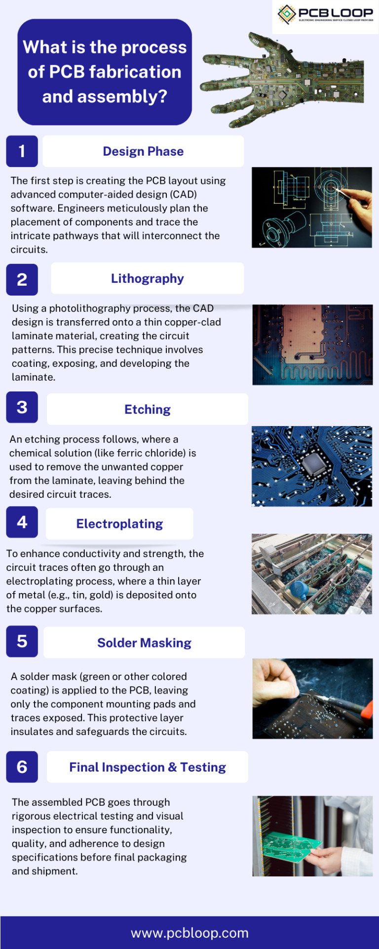
Making printed circuit boards (PCBs) involves several steps. PCBLOOP has been making good PCBs for over 20 years. We focus on giving our customers high-quality products, quick delivery, and good value. We're experts in PCBs and you can trust us. First, we plan the PCB fabricator's layouts carefully on computers. Then, we put the designs on thin copper sheets. Chemicals remove any extra copper, leaving only the circuit traces. Next, we add metal coatings to the circuits to make them stronger and better at conducting electricity. After that, we precisely attach tiny electronic parts to the boards using special soldering machines. Finally, we thoroughly test and check the completed PCBs to ensure they work perfectly. You can learn more about this process by reading our blog post.
1 note
·
View note
Text
#pcb assembly services#circuit board assembly#printed circuit assembly#printed circuit board design#electronic pcb#pcb fabrication and assembly#pcb production#pcb design service#pcb fabrication#pcb electronic#oem electronics manufacturing#pcb prototype us
0 notes
Text
What is a Printed Circuit Board?
Printed Circuit Boards are boards that connect various points together through lines and pads. They allow signals and power to connect between two separate physical devices. While the term “printed circuit board” is typically used, other terms to describe these include “printed wiring board” and “printed wiring card.”

#marketing#investing#finance#branding#pcb circuit#pcb#pc build#pcb assembly#flexible circuit board#pcb board fabrication#pcb circuit design#pcb circuit in Gujarat#pcb design company#Printed Circuit Boards
2 notes
·
View notes
Text
What is PCB Assembly ?
PCB Assembly manufacturer - Hitech Circuits Co., Limited
It’s the step in the manufacturing process in which you populate a blank board with the electronic components needed to make it into a functional printed circuit board. It’s these components that make a board into the circuit that enables an electronic product to function. PCB assembly typically takes place via one of two processes:
1. Surface-mount technology
SMT: SMT stands for “Surface Mount Technology“. The SMT components are very small sizes and comes in various packages like 0201, 0402, 0603, 1608 packages for resistors and capacitors. Similarly for Integrated circuits ICs we have SOIC, TSSOP, QFP and BGA.
The SMT components assembly is very difficult for human hands and can be time taking process so it is mostly done by automated pick and place machine.
2. Through-hole manufacturing
THT: THT stands for “Through hole Technology”. The components with leads and wires, like resistors, capacitors, inductors, PDIP ICs, transformers, transistors, IGBTs, MOSFETS are example.
The component has to be inserted on one side of PCB and pulled by leg on other side and cut the leg and solder it. The THT components assembly is usually done by hand soldering and is relatively easy.
Printed Circuit Board Assembly Techniques
There are only two common PCBA techniques available for use by a PCB designer. The methods are:
1. Automated PCB Assembly Techniques
Generally, this technique employs the use of state of the art machines, which are fully automatic. For example, the surface mount components are worth positioning with the aid of an automated pick and place machine.
Again, reflow soldering is commonly for surface mount components usually done in a reflow oven. An automated solder stencil is also used to apply the solder paste on the PCB.
Finally, high tech inspection machines are used to confirm and check the quality of the PCBA. Some of which include: Automated optical inspection machine (AOI), X-ray inspection machines, etc.
Above all, due to the precise monitoring, control of soldering, no human input and versatile machines.
This technique ensures utmost efficiency, output consistencies, and limits defects.
2. Manual PCB Assembly Techniques
This method is favorite for use with through-hole parts, which needs manual placement on the board. Besides, with these through-hole parts, it’s advisable you use wave soldering. Note that in the through- hole assembly process, you need to place the components and electronics on the PCB.
After that, you use wave soldering to solder the leads. Typically, you will need an individual to insert a component into a marked PTH. Once done, transfer the PCB to the next station where the next person will be on standby tasked with fixing another part.
What are the Benefits of SMT PCB Assembly?
SMT assembly provides many benefits and some of them are as follows:
It can be used to incorporate small components.
In SMT, the components can be placed on both sides of the board.
It assures high component densities.
Fewer holes need to be drilled for surface mounting than through-hole.
It require low initial costs and time for setting up the mass production.
SMT is the simpler and faster-automated assembly when compared to through-hole.
Errors regarding the component placement can be easily rectified.
Surface mount PCBs feature strong joints, which can easily withstand vibrations.
What are the techniques used in Surface Mount Technology?
There are several techniques for the reflow process. After applying the solder paste or a flux mixture on the board and after placing the components, the boards are conveyed to a reflow soldering oven. The techniques used for reflowing soldering include infrared lamps, hot gas convection, fluorocarbon liquids with a high boiling point, and so on.
What are the different testing methods used in SMT PCB Assembly?
Hitech Circuits as the PCB assembly manufacturer, we perform the following testing and inspection to ensure the quality of surface mount PCBs.
Automated Optical Inspection (AOI): This is performed before and after the soldering to identify the component placement, presence, and solder quality.
X-ray Testing: In this type of testing, the operator relies on the X-ray images of the PCB to check the solder joints and lead-less components such as Quad Flat Packs and ball grid arrays, which are generally not visible to naked eyes.
In-Circuit Testing (ICT): This method is used to detect manufacturing defects by testing the electrical properties in the SMT Assembly.
What type of files or documents should I send for SMT PCB Assembly?
Gerber Files: The file contains all details of physical board layers including solder masks, copper layers, drill data, legends, and so on.
Bill of Materials (BOM): This contains information on the list of items needed for the PCB manufacturing and the instructions of manufacturing.
Pick and Place File: This file contains information on all components to be used in the PCB design and their rotation and X-Y coordinates.
The whole process of PCB Assembly
1. Bare board loader machine
The first step in the PCB assembly is to arrange the bare boards on the rack, and the machine will automatically send the boards one by one into the SMT assembly line.
2. Printing solder paste
When PCB on the SMT production line, firstly, we have to print solder paste on it, and the solder paste will be printed on the pads of the PCB. These solder pastes will be melt and solder the electronic parts to the circuit board when it passes through the high-temperature reflow oven.
In addition, when testing new products, some people will use film board/adhesive cardboard instead of solder paste, which can increase the efficiency for adjusting the SMT machines.
3. Solder paste inspection machine(SPI)
Since the quality of solder paste printing is related to the quality of welding of subsequent parts, some SMT factories will use optical machine to check the quality of solder paste after printed the solder paste in order to ensure stable quality. If there any poorly printed solder paste board, we will wash off the solder paste on it and reprint, or remove the excess solder paste if there is redundant solder paste on it.
4. High speed SMT machine
Usually, we will put some small electronic parts (such as small resistors, capacitors, and inductors) to be printed on the circuit board first, and these parts will be slightly stuck by the solder paste just printed on the circuit board, so even if the speed of printing is very fast and the parts on the board will not fall away. But large parts are not suitable for use in such high speed SMT machines, which will slow down the speed of small parts assembly. And the parts will be shifted from the original position due to the rapid movement of the board.
5. Universal SMT machine
Universal SMT machine is also known as "slow machine", it will be assembled some large electronic components, such as BGA IC, connectors, etc., these parts need more accurate positions, so the alignment is very important. Use a camera to take a picture to confirm the position of the parts, so the speed is much slower than High speed SMT machine we taked before. Due to the size of the components here, not all of them are packed in tape and reel, and some may be packed in trays or tubes. But if you want the SMT machine to recognize the trays or tube-shaped packaging materials, you must configure an additional machine.
Generally, traditional SMT machines are using the principle of suction to move electronic parts, and in order to place the parts successfully, and there must be the flat surface on these electronic components for the suction nozzle of the SMT machine to absorb. However, for some electronic parts don’t have a flat surface for these machines, and it is necessary to order special nozzles for these special-shaped parts, or add a flat tape on the parts, or wear a flat cap for thees electronic parts.
6. Manual parts or visual inspection
After assembled all parts by the high speed SMT machine or Universal SMT machine and before going through the high-temperature reflow oven, and we will set up a visual inspection station here and to pick out the deviation parts or missing components boards etc., because we have to use a soldering iron to repair if there are still defectives boards after passing the high-temperature oven, which will affect the quality of the product and will also increase the cost. in addition, for some larger electronic parts or traditional DIP parts or some special reasons cannot be processed by the SMT machine before, they will be manually placed on pcb here.
7. Reflow oven
The purpose of reflow oven is to melt the solder paste and form a non-metallic compound on the component feet and the circuit board, that means to solder electronic components on the circuit board. The temperature rise and fall curves often affect the soldering quality of the entire circuit board. According to the characteristics of the solder materials, usually the reflow oven will set the preheating zone, soaking zone, reflow zone, and cooling zone to achieve the best soldering effect.
For example, the melting point for SAC305 solder paste with lead-free is about 217°C, which means that the temperature of the reflow oven must be higher than the melting points to remelt the solder paste. What's more, the maximum temperature in the reflow furnace should not exceed 250°C, otherwise many parts will be deformed or melted because they cannot withstand such a high temperature.
Basically, after the pcb passed through the reflow oven, the assembly for the entire circuit board is almost complete. If there are hand-soldered parts, we need to transfer to DIP process, and then we have to check the quality after reflow oven by QC department.
8. Automatic optical inspection(AOI)
The main purpose of setting up AOI is because some high density boards can’t be process the following ICT test, so we used AOI inspection to replace it. But even using AOI inspections, there still have the blind spots for such checking, for example, the solder pads under the components cannot be checked by AOI. At present, it can only check whether the parts have side standing issue, missing parts, displacement, polarity direction, solder bridges, lack of soldering etc., but cannot checking the BGA solderability, resistance value, capacitance value, inductance value and other components quality, so far AOI inspection can’t completely replace ICT test.
Therefore, there is still some risk if only AOI inspection is used to replace ICT testing, but ICT test is also not 100% make sure the good quality, we suggest these two ways can be combined with together to make sure the good quality.
9. PCB unloader machine
After the board is fully assembled, it will be retracted to the unloder machine, which has been designed to allow the SMT machine to automatically pick and place the board without damaging the quality for PCB.
10. Visual inspection for finished products
Normally there will be a visual inspection area in our SMT production line whether there is an AOI station or not, and it will help to check if there are any defectives after completed assembled the pcbs. If there is an AOI station, it can reduce the visual inspection worker on our SMT line, and to reduce the potential cost, and because it is still necessary to check some places that cannot be judged by AOI, many SMT factories will provide the mainly visual inspection templates at this station, which is convenient for visual inspection worker to inspect some key parts and polarity for components.
11. DIP process
DIP process is a very important process in the whole PCBA processing, and the processing quality will directly affect the functional for PCBA boards, so it is necessary to pay more attention to the DIP process. There are many preliminary preparations for DIP process. The basic process is to re-process the electronic components first, like to cut the extra pins for some DIP components, our staff received the components according to the BOM list, and will check whether the material part numbers and specifications are correct or not, and performs pre-production pre-processing according to the PCBA samples. The steps are: Use various related equipment (automatic capacitor pins cutting machine, jumper bending machine, diode and triode automatic forming machine, automatic belt forming machine and other machines) for processing.

12. ICT test
Printed Circuit board open/short circuit test (ICT, In-Circuit Test), The purpose of ICT test is mainly to test whether the components and circuits on the printed circuit board are open or short issues. It can also measure the basic characteristics of most components, such as resistance, capacitance, and inductance values to judge whether the functions of these parts are damaged, wrong parts or missing parts etc. after passing through the high-temperature reflow oven.
ICT test machines are divided into advanced and basic machines. The basic ICT test machines are generally called MDA (Manufacturing Defect Analyzer). It’s just to measure the basic characteristics of electronic components and judge open and short circuits issue we talked above.
In addition to all the functions of the basic ICT test machines, for advanced ICT test machine can also test the whole PCBA by using power, start to testing the PCBA boards by setting the program in the test machine. The advantage is that it can simulate the function of the printed circuit board under the actual power-on condition, this test can partly replace the following functional test machine (Function Test). But the cost for the test fixture of this advanced ICT test can probably buy a car, it’s too expensive and we suggest it can be used in mass production products.
13. PCBA function test
Functional testing is to make up for the ICT test, because ICT only tests the open and short circuits on the the PCBA board, and other functions such as BGA and other fuctions are not tested, so it is necessary to use a functional testing machine to test all functions on the whole PCBA board.
14. Cutting board (assembly board de-panel)
Normally, printed circuit boards will be produced in panel, and it will be assembled to increase the efficiency of SMT production. It means several single boards in one panel, such as two-in-one, four-in-one etc. After finished all the pcb assembly process, it needs to be cut into single boards, and for some printed circuit boards with only single boards also need to cut off some redundant board edges.
There are several ways to cut the printed circuit board. You can design the V-cut using the blade cutting machine (Scoring) or directly manually break off the board (not recommended). For more high density circuit boards, it will be used the professional splitting machine or the router to split the board without any damage the electronic components and printed circuit boards, but the cost and working hours will be a little longer.
Why Choose Hitech Circuits PCB Assembly Manufacturer for Your PCB Assembly Projects?
There are several PCB manufacturers specializing in PCB assemblyservices. However, Hitech Circuits PCB Assembly stands out owing to the following:
Assistance in Material Procurement:
Technically, in PCB assembly services, the quality of parts is the responsibility of the OEM; however, we ease your job by assisting you to make the right selection. We can help you procure all your parts of the same type own a single part number, thanks to our supply chain and vendor network as well as experience. This saves time and cost that goes in ordering single parts as you plan.
Testing procedures:
We are very focused on quality and thus implement stringent testing procedures at each stage of the assembly and after completion.
Fast Turnaround Times:
Our well-equipped facility and the right tools enable us to complete your requirements well before time, and without compromising on the quality or functioning of the PCBs. For simple designs we revert in 24 to 48 hours.
Cost Effectiveness:
While PCB assembly is a cost-effective alternative, we go a step further and assure that the parts you list are of a good quality and suitable for your requirement. Also, you can control the part flow and replenish them as needed. This eliminates the need to buy extra stock and store it.
Quick Quote:
We offer a quick quote based on your BOM. All you need is a detailed BOM, Gerber files, your application requirement sheet, and quantity.
We’re not one to stand still, which is why we use the latest equipment and the finest minds to create your PCB projects. We’re constantly keeping our finger on the pulse of the latest trends. And as a result, we know how to deliver the highest standards of PCB assembly to meet all your requirements.
Our dedicated, friendly customer service team also means that we support you every step of the way. Offering our expert guidance to ensure a complete PCB project that you’re happy with.
Contact us today
No matter what your printed circuit board assemblyneeds are, we always aim to deliver efficient, dependable solutions. For more information about our services, do not hesitate to get in touch with us today for a no-obligation quote
2 notes
·
View notes
Text
The Impact of Robotics and Automation on Printed Circuit Board (PCB) Assembly
Robotics and automation have become integral in various sectors, including the electronics industry. These innovations have significantly transformed how PCB assembly services operate. Here’s how:
Improving Quality and Consistency
Robotics and automation have brought remarkable quality improvements in PCB assembly. Robots have surpassed human capabilities in terms of precision and consistency, significantly reducing errors associated with manual assembly.
High-tech cameras and sensors built into these robots can detect and rectify errors in real time, ensuring the production of high-quality PCBs.
This consistent precision is particularly crucial for complex and miniaturized boards, where even minor errors can lead to significant operational issues.
Increasing Production Speed
The speed of PCB assembly has been substantially enhanced with the introduction of automation. Robots can perform tasks much faster than their human counterparts, without breaks or slowdowns.
As a result, the turnaround time for PCB production has drastically reduced, making it possible for manufacturers to meet high-demand requirements efficiently. Automated machines can work around the clock, ensuring continuous production and timely delivery.
Enhancing Worker Safety
The electronics industry often involves dealing with hazardous materials and processes that pose risks to human operators. Robotics and automation have minimized these risks by taking over the dangerous tasks.
Robots are immune to hazardous substances and can operate in high-temperature environments without any health risks. This ensures a safer working environment, reducing accidents and improving worker morale.
Reducing Costs
While the initial setup cost of automated machinery and robots may be high, the long-term benefits significantly outweigh these costs.
Quick turn PCB fabrication reduces production time, saves on labor costs, and minimizes waste due to fewer errors.
What’s more, the high precision of robotic assembly reduces the need for reworks, further saving costs. Thus, automation is a cost-effective solution for PCB manufacturers in the long run.
Promoting Scalability
With robotics and automation, PCB manufacturers can easily scale up their operations to meet increasing demand. Automated machines can be programmed to perform a variety of tasks, making them adaptable to different production requirements.
Unlike manual labor, scaling up with robotics doesn't require extensive training or additional personnel. This makes it a more efficient and flexible solution.
As we continue advancing technologically, robotics and automation's role in PCB assembly is only expected to grow.Bay Area Circuits (BAC) provides top-notch PCB layout design, fabrication, and assembly services. BAC has been in the industry for over four decades. The company has earned certifications such as ISO-9001 and ITAR, indicating their commitment to quality. Contact BAC to get a quote.
0 notes
Text
Viasion offers high-quality PCB fabrication services. Explore our advanced manufacturing capabilities and reliable solutions for your printed circuit board needs.
0 notes
Text
Unveiling the advantages and disadvantages of Surface Mount Technology (SMT)
Introduction
Printed circuit board assembly, in particular, has significantly benefited from surface mount technology (SMT). SMT eliminates the requirement for drilled holes and manual insertion by mounting electronic components directly onto a PCB's surface. This technique offers several advantages, such as smaller and thinner PCBs, flexibility in design, reduced material costs, simplified automation, and high signal transmission capabilities.
Advantages of SMT in PCB Assembly
Ultra-Thin and Miniature PCBs
The size and weight of surface-mount components are significantly lower than their through-hole counterparts. Boards are smaller and thinner because their compactness makes better use of space on printed circuit boards. As a result, products can be designed to be more compact without compromising functionality or performance.
Flexibility
SMT provides great flexibility in terms of PCB materials and designs. It enables the use of flexible PCBs (flex PCBs) and rigid-flex PCBs that can bend or conform to specific shapes or spaces. This flexibility opens up opportunities for innovative designs while maintaining excellent electrical performance.
Lesser Expense on Materials and Cardboard
Unlike through-hole components that require manual insertion, SMD components can be automatically placed on the board using pick-and-place machines or automated assembly lines. This automation streamlines the production process, reduces labour costs, and improves efficiency.
Simplified Manufacturing Process
When compared to through-hole components, surface-mount devices (SMDs) can be automatically positioned on the board through the use of pick-and-place machines or automated assembly lines. Because of this automation, production is more streamlined, costs less to operate, and more efficient overall.
Frequency and High Signal Transmission
Fast signal transmission with less radio frequency interference is made possible using SMT components, which are compatible with high-density double-sided and multi-layer printed circuit board assembly. Additionally, SMT assemblies' lack of leads improves their resilience to vibration and guarantees dependable signal integrity.
Drawbacks of SMT for PCB Build-Up
High Initial Investment
Implementing SMT assembly requires investment in specialized equipment such as reflow ovens, solder paste screen printers, pick-and-place machines, and hot air rework stations. These machines can be costly but are essential for efficient and accurate assembly.
Difficult to Inspect
Due to the small sizes and numerous solder joints of most SMD components, inspection becomes challenging. Identifying defects or faults can be time-consuming, especially when dealing with complex packages like ball grid arrays (BGAs), where solder balls are located under the component.
Fragility
Comparing surface-mount components to their through-hole counterparts, SMD parts are more delicate and fragile. They can be easily damaged if mishandled or dropped during the manufacturing process or while in use. Special care must be taken to handle and package these components using anti-static measures in clean room environments.
Expensive Small Batch Production
Technical complexity necessitates skilled operators and specialized equipment, making prototyping or small-batch manufacture of SMT PCBs an expensive ordeal. Due to the high initial setup expenses, SMT technology may not be cost-effective for small volumes.
Limited Power Capabilities
Surface mount technology isn't suitable for all electrical components, active or passive, because of power constraints. Components generating high heat may not be suitable for surface mounting as it can cause solder melting and compromise the integrity of the connection.
Despite these challenges, SMT remains a highly recommended practice in the manufacturing industry due to its numerous benefits. It enables manufacturing efficiency, design flexibility, better performance in harsh conditions or high-frequency applications, and more compact devices without compromising functionality or performance attributes. With ongoing advancements and innovations in SMT technology aimed at addressing existing limitations and improving production processes further, we can expect to see continued growth and impact on the industry.
This Blog Originally Posted Here: https://www.pcbpower.us/blog/unveiling-the-advantages-and-disadvantages-of-surface-mount-technology
0 notes
Text
Investing in Reliable Electronics Assembly and Fabrication Services is Beneficial
Another benefit is optimizing the process of sourcing PCB devices and fabrication services in a highly cost-effective manner. You can control the budget for the project without any hassles. The flexible PCB cost doesn’t go through the roof. You can keep the expense down. It is more sustainable from a long-term perspective.
#PCB Assembly Fabrication#PCB Assembly#PCB#rigid flex printed circuit boards#flexible pcb#printed circuit board assembly services#printed circuit board company
0 notes
Text
Do you know how to test CHF 100A CPU cards ?
#vfd #inverter #converter #test
1 note
·
View note
Text
Best Electronics Contract Manufacturing Services - PCBLOOP
PCBLOOP is the leading electronics manufacturing service provider in China. Our main goal is to deliver electronic engineering design and manufacturing services throughout the world. Our main services are prototype design, PCB fabrication, PCB assembly, components sourcing, injection molding, final product assembly, etc. Visit our website for more information about our services.
Website - https://www.pcbloop.com

1 note
·
View note
Text
DESIGN PCB WITH ALTIUM PCB DESIGNER
Altium Designer is a complete solution for PCB projects, from basic circuits to full avionics systems. With tools for design rule management, advanced routing, and 3D surface design, you can efficiently navigate complexities and control costs.

#Altium Designer#circuit board manufacturers near me#pcb circuit board manufacturers in india#pcb fabrication near me#pcb board fabrication#pcb circuit design#pcb circuit in Gujarat#pcb assembly company in india#top pcb manufacturers#pcb stencils#pcb design company#pcb circuit board
0 notes
Text
Introducing iNPACK™ Our Miniaturization Solutions Business Unit. Specializing in Organic Substrates & Advanced Packaging Check out our recent customer conference video at PCB Technologies!
It was a huge success, showcasing our capabilities and expertise in miniaturization, substrate production, and more. Over 140 professionals attended and the level of engagement was outstanding.
We have gone from a mini-manufacturer to a full-full-fielded development center for our customers and received valuable feedback reinforcing our company's worth.
https://www.pcb-technologies.com/
#pcbdesign#packaging#packagingdesign#BeyondDesignLimits#pcb assembly services#pcb fabrication#PCB#reliabilityengineering#microelectronics#QTA#sip#substrates#miniaturization
0 notes
Text
SMT production process

Program the SMT placement machine
According to the BOM position map provided by the customer, program the coordinates of the location of the components. Then carry out the first piece with the SMT chip processing data provided by the customer.
Printing solder paste
The solder paste is stenciled to the PCB board where the electronic component SMD needs to be soldered to prepare for the soldering of the components. The equipment used is a screen printing machine (printing machine), which is located at the forefront of the SMT chip processing production line.
SPI
Solder paste detector, detects whether the solder paste printing is a good product, whether there is less tin, leaking tin, more tin and other undesirable phenomena.
4.SMT
Accurately install the electronic components SMD on the fixed position of the PCB. The equipment used is a placement machine, which is located behind the screen printing machine in the SMT production line.
The placement machine is divided into high-speed machine and general-purpose machine.
High-speed machine: used to paste components with large pin spacing and small pin spacing
Universal machine: paste small pin pitch (pin density), bulky components.
High temperature solder paste melting
Mainly, the solder paste is melted at high temperature, and after cooling, the electronic components SMD and the PCB board are firmly welded together. The equipment used is a reflow soldering furnace, which is located behind the placement machine in the SMT production line.
AOI
Automatic optical detector to detect whether the soldered PCBA components have poor soldering, such as tombstone, displacement, empty soldering, etc.
Visual inspection
The key items of manual inspection and inspection: whether the PCBA version is the changed version; whether the customer requires components to use substitute materials or components of designated brands and brands; IC, diodes, triodes, tantalum capacitors, aluminum capacitors, switches, etc. Whether the direction of the directional components is correct; defects after welding: short circuit, open circuit, fake parts, fake welding.
Packaging
Products that have passed the test will be packaged separately. The commonly used packaging materials are anti-static bubble bags, electrostatic cotton, and blister trays. There are two main packaging methods, one is to use anti-static bubble bags or electrostatic cotton into rolls, which are the most commonly used packaging methods at present; the other is to customize blister trays according to the size of PCBA. Put it in a blister tray and unpack it, mainly for PCBA boards that are sensitive and have vulnerable patch components.
0 notes
Text
PCB Manufacturer - Online PCB Board Design | PCB Power Market
#PCB Power Market is India’s leading online PCB board manufacturer We provide PCB manufacturing services#PCB Design#PCB fabrication#and PCB assembly
0 notes
Text
PCB Manufacturing Process In Usa
A crucial phase in any PCB fabrication and assembly process is inspection. Defects are found through inspection, and once they are fixed the operation as a whole is improved. It also aids in identifying design faults that already exist. Finding problems before moving on to the next step is made possible by inspecting PCBs after each stage of the process. Eliminating defects needs significantly less time and effort than fixing a flawed product after it has been used in the market. The inspection procedure supports the manufacturer's reputation, fosters consumer confidence, and helps assure constant product quality.
0 notes
Text
The Impact of PCB Assembly on Miniaturization
In the early days of personal computing, computers were massive machines that occupied entire rooms. They had limited processing power and were mainly used for complex calculations and data processing. Users interacted with them through punch cards and command-line interfaces.
Now, fast forward to the present day, where personal computers have undergone a remarkable transformation. Today's computers are sleek, powerful devices that can fit on a desk or even in your backpack. Moreover, these modern computers are not just tools for number crunching. They are multimedia powerhouses & provide access to the vast expanse of the internet, enabling communication, research, and information sharing.
A Deeper Dive into PCB Miniaturization
The process of miniaturization in electronic devices involves condensing more transistor nodes onto smaller integrated circuits (ICs). Once integrated, these ICs become part of a system or device, enabling it to perform its intended function. This technology achieves a remarkable combination of reduced size and increased power.
The evolution of miniaturization aligns with Gordon Moore's foresight in 1965, predicting that integrating more components onto ICs would lead to innovations such as home computers, automotive controls, and portable communication devices. Moore's prediction materialized, ushering in an era of technological advancements, including portable computers, smartphones, medical devices, the Internet of Things, 5G wireless devices, as well as AR/VR and AI—all made possible by smaller yet more powerful computing systems.
While envisioning these miniature technologies is one aspect, the manufacturing process presents its own set of challenges. Electronics manufacturers continually innovate to overcome these challenges and fulfil the promises of miniaturization.
Miniaturization holds the potential to revolutionize the world, but realizing this potential requires advanced manufacturing processes, such as advanced electronics assembly. It involves a meticulous blend of expertise, precision, and innovative processes to transition from conceptualization to mass production and global distribution.
Evolution of Miniaturization
A notable miniaturization technique involves using Ball Grid Arrays (BGAs) for integrated circuit packages. BGAs facilitate numerous connections between the integrated circuit and the printed circuit board, enhancing signal routing and processing power. They also contribute to chip reliability and heat reduction, making them integral to technology miniaturization.
Miniaturization with Advanced PCB Assembly
Additionally, wafer-level chip scale packages (WLCSPs) play a role in miniaturization by creating micro-scale ICs on a wafer, which are later diced into individual chips. These packages, often featuring gold joints, maintain reliability even at tiny scales, enabling downsizing without compromising performance. The Chip-on-Board (CoB) process is another crucial element in advanced electronics assembly, involving the specialized attachment of integrated circuit chips to substrates. This process becomes particularly intricate as the size and shape of ICs and substrates vary significantly among different products.
The Road Ahead
In essence, miniaturization holds the promise of addressing significant global challenges, from extending human life to powering cleaner energy solutions. Advanced electronics assembly acts as the bridge between groundbreaking research and consumer accessibility, enabling seamless transitions from prototypes to production, regardless of the complexity or size of the electronics involved. Whether a startup or a Fortune 500 technology leader, we offer advanced PCB assembly services that ensures a smooth journey.
This blog published originally here: https://www.pcbpower.us/blog/the-impact-of-pcb-assembly-on-miniaturization
0 notes
Last Seen Blogs

inum4ki
Untitled

ekarigartech
Equipments|Agricultural|Ecommerce|Lighting|Tech

nighty-night-nh
🌿Keepin'🏳️🌈Cozy🌿

vi-talks
moved to @lovecountdownz

icareaboutme
peace