#semiconductor wafer fabrication
Text
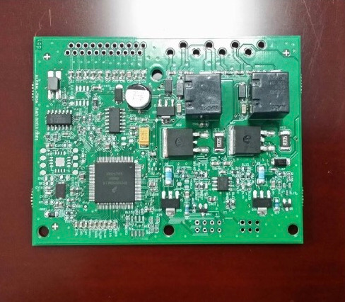
Exploring the Intricacies of Semiconductor Wafer Fabrication and Piping
Dive deep into the fascinating world of semiconductor technology! Learn about the intricate processes behind semiconductor wafer fabrication and the crucial role of semiconductor piping in this fast-paced industry. Discover the cutting-edge innovations shaping our digital future.
#process piping systems#semiconductor solutions#manufacturing piping solutions#off-site manufacturing#semiconductor#piping manufacturing#process piping services#semiconductor wafer fabrication
0 notes
Text
The Growing Demand of Semiconductor Equipment Driving Innovation

Semiconductors: Enabling Modern Technologies
Semiconductors are one of the most important components of modern electronics. They are the building blocks of technologies such as smartphones, computers, vehicles, appliances and more. As technologies become more advanced and integrated into our daily lives, the demand for semiconductors keeps rising exponentially. This growing demand is driving constant innovation in Semiconductor Device which is essential for manufacturing these tiny yet powerful components.
Semiconductor Equipment fabrication requires sophisticated manufacturing processes and precise equipment. Semiconductor Device manufacturers are continuously working to develop more advanced tools that can produce smaller, more powerful and energy-efficient semiconductors. Some of the key equipment types and technologies enabling advances in semiconductor manufacturing are discussed below.
Lithography Systems: Enabling Smaller Circuit Designs
Lithography systems are used to transfer electronic circuit patterns onto silicon wafers during the semiconductor fabrication process. As circuits continue to shrink in size to accommodate more transistors in a tiny space, lithography technology needs to keep pace. The mainstream lithography technology currently used is extreme ultraviolet (EUV) lithography which uses short wavelength EUV light to print ever smaller microscopic circuits.
EUV lithography allows semiconductor manufacturers to print minimum features less than 10 nanometers across. Equipment manufacturers are ramping up EUV lithography machine manufacturing to support the transition to this advanced technology needed for the latest and future generations of semiconductors. Several companies are also developing next-generation lithography technologies like nanoimprint lithography and electron-beam lithography to take circuit scaling even further below 10nm.
Deposition Equipment: Laying Down Thin Film Layers
Semiconductor manufacturing involves depositing extremely thin layers of various materials like silicon, insulators, polymers or metals onto silicon wafers through deposition processes. Chemical vapor deposition (CVD) and physical vapor deposition (PVD) are commonly used deposition techniques in the industry.
Semiconductor Equipment manufacturers are continuously optimizing deposition systems to achieve ultra-thin yet highly uniform film layers. They are building systems that offer superior step coverage to deposit films of various materials into narrow trenches and holes on complex 3D circuit designs. Advanced deposition technologies like atomic layer deposition (ALD) that allows conformal deposition one atomic layer at a time is also gaining traction for manufacturing next-generation semiconductors.
Etch Systems: Sculpting Circuit Patterns
Etch systems play a vital role in semiconductor manufacturing by selectively "removing" excess deposited material to reveal the desired circuit patterns on wafers. Different etch techniques like wet etching, plasma etch and reactive ion etching are used.
As circuit features shrink to nanometer scales, etch equipment must sculpt intricate 3D structures with atomic-level precision and uniformity. Chipmakers are adopting sophisticated plasma etch systems equipped with novel process chemistries, variable frequency plasma sources and endpoint detection tools for higher resolution and selectivity. Equipment vendors are engineering etch systems optimized for materials like metals, dielectrics and compound semiconductors to enable the complex multilayered architectures of tomorrow's advanced chips.
Wafer Inspection and Metrology Tools Enabling Quality Control
Error-free manufacturing of sub-10nm semiconductor structures requires comprehensive quality control. Metrology and inspection tools analyze fabricated wafers throughout the process to detect defects or quantify if critical dimensions meet tight specifications.
As circuitry becomes smaller, inspection systems equipped with powerful optics, imaging techniques and sensors down to angstrom resolutions are essential. Metrology tools employ techniques like scatterometry, medium-energy ion scattering etc to non-destructively characterize tiny structures and film layers. Automated defect inspection tools scanning whole wafer surfaces help reduce costly reworks. These enabling tools will continue scaling capabilities in lock-step with chip architectures.
Meeting the Cleanroom Challenges of Advanced Node Fabrication
Another challenge is managing the contamination control, temperature, humidity and airflows needed for fabricating ever smaller circuits in tightly controlled cleanroom environments. Equipment vendors provide solutions like mini- and macro-environments, advanced filter technologies along with real-time environmental monitoring systems. This helps manufacturers achieve the stringent international cleanroom specifications required at under 10nm process nodes.
Role of Semiconductor Device in Innovation
Innovations happening at the level of Semiconductor Equipment underpin ongoing progress in chip technology and the transformation of daily technology products. Continuous advancements are essential to produce smaller, more powerful semiconductors powering capabilities like artificial intelligence, augmented reality and autonomous systems. Rapidly evolving equipment solutions from lithography to metrology demonstrate the collaborative innovation between chipmakers and equipment vendors necessary to sustain Moore's Law scaling. This ensures semiconductors remain a driver for breakthrough technologies of the future.
Get More Insights On, Semiconductor Equipment
About Author:
Money Singh is a seasoned content writer with over four years of experience in the market research sector. Her expertise spans various industries, including food and beverages, biotechnology, chemical and materials, defense and aerospace, consumer goods, etc. (https://www.linkedin.com/in/money-singh-590844163)
#Semiconductor Manufacturing#Wafer Fabrication#Cleanroom Technology#Packaging and Assembly#Lithography Equipment
0 notes
Text

#bunny girl#my bedroom is a class 100 cleanroom#semiconductor wafer fabrication play#I'm not even sure if this joke is very funny but working for a semiconductor company for two years broke my soul at a fundamental level
1 note
·
View note
Text
Chinese scientists have made a significant breakthrough in the world of semiconductors, the South China Morning Post (SCMP) reports. Just one atom thick (thereby termed "2D"), the new 12-long (30.5 cm) wafers can be cheaply and potentially revolutionize the semiconductor industry, its creators claim. While more work is needed to turn them into usable microchips, the new wafers could complement, even challenge, traditional silicon chips.
Due to its thinness, the new 2D material exhibits superior semiconducting properties. However, the team of scientists faced challenges when it came to scaling up the size of the wafers and producing them in large quantities. “We proved to the industry that this is scientifically feasible and instilled confidence. If there are industrial demands in the future, progress in this field will advance by leaps and bounds,” study lead Professor Liu Kaihui of Peking University told SCMP in an exclusive interview.
As reported in a study published in Science Bulletin, the new wafers offer some critical improvements over existing silicon chips. “When silicon transistors are made thinner, their [voltage control] becomes worse. Current will exist even when the device is not working. This brings extra energy costs and heat generation,” Liu explained.
The new 2D material comprises crystalline solids with one or several atom layers. Due to its naturally atomic-level thickness, the wafers possess unique physical properties and have potential applications in high-performance electronic devices. “A transistor built from a single layer of MoS2, [a typical 2D material] with a thickness of about one nanometre, outperforms the one made with the same thickness of silicon many times,” Liu added.
[...] to date, scientists have struggled to fabricate 2D material wafers with high uniformity and device performance, even though 2D materials can exist separately at each layer. The new wafers can be stacked layer by layer, including materials such as graphene or transition metal dichalcogenides (TMDs) like molybdenum disulfide, tungsten disulfide, molybdenum diselenide, and tungsten diselenide.
28 Aug 23
37 notes
·
View notes
Photo

Engineers 'grow' atomically thin transistors on top of computer chips
Emerging AI applications, like chatbots that generate natural human language, demand denser, more powerful computer chips. But semiconductor chips are traditionally made with bulk materials, which are boxy 3D structures, so stacking multiple layers of transistors to create denser integrations is very difficult.
However, semiconductor transistors made from ultrathin 2D materials, each only about three atoms in thickness, could be stacked up to create more powerful chips. To this end, MIT researchers have now demonstrated a novel technology that can effectively and efficiently "grow" layers of 2D transition metal dichalcogenide (TMD) materials directly on top of a fully fabricated silicon chip to enable denser integrations.
Growing 2D materials directly onto a silicon CMOS wafer has posed a major challenge because the process usually requires temperatures of about 600 degrees Celsius, while silicon transistors and circuits could break down when heated above 400 degrees. Now, the interdisciplinary team of MIT researchers has developed a low-temperature growth process that does not damage the chip. The technology allows 2D semiconductor transistors to be directly integrated on top of standard silicon circuits.
Read more.
#Materials Science#Science#Transistors#Electronics#2D materials#Transition metal dichalcogenides#Temperature#Circuits#MIT
24 notes
·
View notes
Text
After four years of watching Donald Trump inflict flesh wounds on China with his ineffectual trade war, U.S. President Joe Biden appears to have found the jugular. The goal is the same, but this knife is sharper—and could set back China’s tech ambitions by as much as a decade.
The target: semiconductor chips, especially the cutting-edge variety used for supercomputers and artificial intelligence. New export controls announced by the Biden administration this month prohibit the sale of not only those chips to China but also the advanced equipment needed to make them, as well as knowledge from any U.S. citizens, residents, or green card holders.
The chips, wafer-thin and the size of a fingernail, underpin everything from our smartphones to the advanced weapons systems that the United States specifically called out in its filing announcing the export restrictions. Perhaps more important—and this is where the U.S. curbs will hurt China the most—they are indispensable to the technologies of the future, such as AI and self-driving cars, as well as virtually every industry from pharmaceuticals to defense.
“You can pick a cliche—people talk about it as the ‘new oil’ or whatever,” said Raj Varadarajan, a managing director and senior partner at the Boston Consulting Group whose research has focused on the semiconductor industry. “But it’s there in everything, it’s pervading everything, and that’s one of the reasons it’s become such a flashpoint.”
China has set out lofty ambitions for its technology sector, with several government plans over the past decade setting out targets such as self-sufficiency in high-tech manufacturing by 2025, global leadership in AI by 2030, and global industry standards dominance by 2035. The latest U.S. broadside is aimed squarely at that “Made in China” sign.
“I think this is part of also signaling to China that we are not just going to resolve to give China global leadership in some of these key areas,” said Daniel Gerstein, a senior policy researcher at the Rand Corp. who previously served in the U.S. Department of Homeland Security’s Science and Technology Directorate. “We don’t want to lose and become beholden, if you will, to Chinese approaches.”
The semiconductor industry is the cornerstone of that strategy, and China has made significant strides in the recent past. The country now accounts for 35 percent of the global market, according to the Semiconductor Industry Association (SIA). But that figure reflects the final sales of finished chips to electronics companies, many of which have large manufacturing operations concentrated in China. The more high-tech and critical parts of the process, such as chip design and initial production, are still dominated by the United States.
And while China can hold its own at the lower end of the spectrum and the production of older-generation chips, it still lags behind in the cutting-edge research, design, and advanced technology that the Biden administration’s export restrictions target. Those goals have now likely been pushed back several years.
A significant reason for China’s vulnerability, as well as its painstaking effort to achieve independence, is how interconnected the global semiconductor supply chain is. Chips will often be designed in one country; fabricated in another using machines from a third; tested in a fourth; and finally assembled and placed into electronic devices in a fifth—sometimes with a few more countries and steps in between.
And many of those countries have concentrated their strengths and capacities in certain parts of that process, creating potential bottlenecks that can easily be exploited. For instance, the SIA estimates that there are “more than 50 points across the value chain where one region holds more than 65% of the global market share.” And 92 percent of manufacturing capacity for the world’s most advanced chips is concentrated in Taiwan; the remaining 8 percent is in South Korea.
The United States is trying to hedge its bets on that front as well, passing the CHIPS and Science Act this year, which provides $52 billion in incentives—most of it for companies that set up chip factories on U.S. soil—and hundreds of billions of dollars more to further shore up its research and development capabilities. Biden has been doing the rounds in upstate New York this month, touting the impact of the act, including at an IBM plant in Poughkeepsie (a day before the export controls were announced) and a Micron facility in Syracuse on Thursday.
For the United States, building up its own manufacturing ecosystem is a fail-safe. For China, it has rapidly become an absolute necessity.
“This is an effort that is going to take hundreds of billions of dollars and an incredible amount of engineering talent and energy to recreate a semiconductor supply chain that doesn’t involve U.S. technology,” said Jordan Schneider, a senior analyst at the Rhodium Group. “This supply chain is so globalized, but also so specialized, that at any step in it there’s only a handful of firms in the world that can do it, and if you’re sort of locked out of any one of these steps, then you can’t make chips.”
There are still some unanswered questions, including how the restrictions will be implemented in practice. In many cases, they give companies the option to apply for licenses to use and sell U.S. technology.
“It’s not clear that permission will be denied. It’s very possible that permission will be given, and so it’ll just delay and slow down some things,” Varadarajan said.
The other big question is whether and how China might hit back. Beijing has slammed what it calls “abuse” of export controls and warned that the restrictions could ultimately “backfire” on Washington, but its response so far has been a distant cry from the tit-for-tat tariffs that were a hallmark of Trump’s trade war.
With semiconductors specifically, the vast gap between U.S. and Chinese technological capabilities means Beijing doesn’t have much with which to retaliate. While China accounts for a significant portion of mature node chips—older, larger semiconductors that are not as cutting-edge but are used in products such as cars—it is not indispensable, and production can likely shift elsewhere without much disruption.
“If the U.S. bans selling semiconductors to China, and China says [it is also] going to ban semiconductors, there isn’t much in terms of things that they make over there that they can ban equivalent to proportional response,” Varadarajan said.
China, in any event, is backed into a corner. Any move Beijing makes at the moment to cut itself off from the global supply chain could hit the country’s employment and exports, both of which it can ill afford with a current economic growth rate of 3 percent—far lower than government forecasts—and no easy way out.
Actions within China in the weeks after the U.S. export controls were announced betray the uncertainty within of what to do next. The Chinese government reportedly held emergency meetings with the country’s top semiconductor firms to assess the impact of the restrictions. The Financial Times reported that one of the leading firms, Yangtze Memory Technologies Corp., has already asked several American employees to leave.
China will be forced to double down on its yearslong effort to build its own semiconductor ecosystem and might just achieve its goal of becoming self-sufficient in the long run. But in the short term, there’s likely to be pain.
“The Chinese companies are going to have an enormously difficult time trying to push past these limits without U.S. technology, but any effort to do so just to get to a 2022 level will probably take a decade or more,” Schneider said. “And even with all the effort, it’s not clear that they would succeed.”
4 notes
·
View notes
Text
Semiconductor Market - Forecast (2022 - 2027)
Semiconductor market size is valued at $427.6 billion in 2020 and is expected to reach a value of $698.2 billion by 2026 at a CAGR of 5.9% during the forecast period 2021-2026. Increased investments in memory devices and Integrated circuit components are driving technological improvements in the semiconductor sector. The emergence of artificial intelligence, internet of things and machine learning technologies is expected to create a market for Insulators as this technology aid memory chip to process large data in less time. Moreover demand for faster and advanced memory chip in industrial application is expected to boost the semiconductor market size. Semiconductors technology continues to shrink in size and shapes, a single chip may hold more and more devices, indicating more capabilities per chip. As a result, a number of previously-used chips are now being combined into a single chip, resulting in highly-integrated solutions. Owing to such advancement in technology the Gallium arsenide market is expected to spur its semiconductor market share in the forecast period.
Report Coverage
The report: “Semiconductor Market Forecast (2021-2026)”, by IndustryARC covers an in-depth analysis of the following segments of the Semiconductor market report.
By Components – Analog IC, Sensors, MPU, MCU, Memory Devices, Lighting Devices, Discrete Power Devices, Others
By Application – Networking & Communication, Healthcare, Automotive, Consumer electronic, Data processing, Industrial, Smart Grid, Gaming, Other components
By Type - Intrinsic Semiconductor, Extrinsic Semiconductor
By Process- Water Production, Wafer Fabrication, Doping, Masking, Etching, Thermal Oxidation
By Geography - North America (U.S, Canada, Mexico), Europe (Germany, UK, France, Italy, Spain, Belgium, Russia and Others), APAC(China, Japan India, SK, Aus and Others), South America(Brazil, Argentina, and others), and RoW (Middle east and Africa)
Request Sample
Key Takeaways
In component segment Memory device is expected to drive the overall market growth owing to on-going technological advancement such as virtual reality and cloud computing.
networking and communication is expected hold the large share owing to rise in demand for smart phone and smart devices around the world.
APAC region is estimated to account for the largest share in the global market during the forecast period due to rise of electronic equipment production and presence of large local component manufacturers.
Semiconductor Market Segment Analysis- By Component
Memory device is expected to drive the overall market growth at a CAGR of 6.1% owing to on-going technological advancement such as virtual reality and cloud computing. High average selling price of NAND flash chips and DRAM would contribute significantly to revenue generation. Over the constant evolution, logic devices utilised in special purpose application particular signal processors and application specific integrated circuits are expected to grow at the fastest rate.
Inquiry Before Buying
Semiconductor Market Segment Analysis - By Application
With increasing demand for smart phone and smart devices around the world networking and communication segment is expected hold the large share in the market at 16.5% in 2020. Moreover due to Impact of Covid 19, the necessity of working from home has risen and the use of devices such as laptops, routers and other have increased which is expected to boost the semiconductor market size. The process of Wafer Level Packaging (WLP), in which an IC is packaged to produce a component that is nearly the same size as the die, has increased the use of semiconductor ICs across consumer electronics components owing to developments in silicon wafer materials.
Semiconductor Market Segment Analysis – By Geography
APAC region is estimated to account for the largest semiconductor market share at 44.8% during the forecast period owing to rise of electronic equipment production. Due to the extensive on-going migration of various electrical equipment and the existence of local component manufacturers, China is recognised as the region's leading country. The market in North America is expected to grow at a rapid pace, owing to rising R&D spending.
Schedule a Call
Semiconductor Market Drivers
Increase in Utilization of Consumer Electronics
Rise in technological advancement in consumer electronic devices have created a massive demand for integrated circuit chip, as these IC chip are used in most of the devices such as Smartphones, TV’s, refrigerator for advanced/ smart functioning. Moreover investment towards semiconductor industries by the leading consumer electronics companies such as Apple, Samsung and other is expected to boost the semiconductor market share by country. The adoption of cloud computing has pushed growth for server CPUs and storage which is ultimately expected to drive the semiconductor market. Wireless-internet are being adopted on a global scale and it require semiconductor equipment As a result, the semiconductor market research is fuelled by demand and income created by their production.
AI Application in Automotive
Semiconductor industry is expected to be driven by the huge and growing demand for powerful AI applications from automotive markets. Automakers are pushing forward with driverless vehicles, advanced driver assistance systems (ADAS), and graphics processing units (GPUs) which is estimated to boost the semiconductor market size. Furthermore, varied automobile products, such as navigation control, entertainment systems, and collision detection systems, utilise automotive semiconductor ICs with various capabilities. In the present time, automotive represents approximately 10 – 12 per cent of the chip market.
Buy Now
Semiconductor Market- Challenges
Changing Functionality of Chipsets
The semiconductor market is being held back by the constantly changing functionality of semiconductor chips and the unique demands of end-users from various industries. The factors such as Power efficiency, unrealistic schedules, and cost-down considerations are hindering the semiconductor market analysis.
Semiconductor Market Landscape
Technology launches, acquisitions and R&D activities are key strategies adopted by players in the Semiconductors Market. The market of Electrical conductivity has been consolidated by the major players – Qualcomm, Samsung Electronics, Toshiba Corporation, Micron Technology, Intel Corporation, Texas Instruments, Kyocera Corporation, Taiwan Semiconductor Manufacturing, NXP Semiconductors, Fujitsu Semiconductor Ltd.
Acquisitions/Technology Launches
In July 2020 Qualcomm introduced QCS410 AND QCS610 system on chips, this is designed for premium camera technology, including powerful artificial intelligence and machine learning features.
In November 2019 Samsung announced it production of its 12GB and 24GB LPDDR4X uMCP chip, offering high quality memory and data transfer rate upto 4266 Mbps in smartphones
In September 2019 the new 5655 Series electronic Board-to-Board connectors from Kyocera Corporation are optimised for high-speed data transfer, with a 0.5mm pitch and a stacking height of under 4mm, making them among the world's smallest for this class of connector.
For more Electronics related reports, please click here
3 notes
·
View notes
Text
Chip, semiconductor, integrated circuit, do you know the relationship and difference between them
1、 What is a chip
Chip, also known as microcircuit, microchip, integrated circuit (IC), refers to the silicon chip containing integrated circuit, which is very small and often a part of computer or other electronic equipment.
Chip is the general term of semiconductor component products. It is the carrier of integrated circuit (IC), which is divided by wafer.
A silicon chip is a small piece of silicon containing an integrated circuit, which is part of a computer or other electronic equipment.
2、 What is semiconductor
Semiconductors refer to materials with conductivity between conductors and insulators at room temperature. For example, diodes are devices made of semiconductors. Semiconductor is a material whose conductivity can be controlled from insulator to conductor.
Whether from the perspective of science and technology or economic development, the importance of semiconductors is very great. Today, the core units of most electronic products, such as computers, mobile phones or digital recorders, are closely related to semiconductors. Common semiconductor materials include silicon, germanium, gallium arsenide, etc., and silicon is one of the most influential semiconductor materials in commercial applications.
There are many forms of matter, such as solid, liquid, gas, plasma, etc. We usually call materials with poor conductivity, such as coal, artificial crystals, amber, ceramics, etc., insulators. Metals with good conductivity, such as gold, silver, copper, iron, tin, aluminum, are called conductors. The material between conductor and insulator can be simply called semiconductor
3、 What is integrated circuit
Integrated circuit is a kind of micro electronic device or component. Using a certain process, the transistors, resistors, capacitors, inductors and other components and wiring required in a circuit are interconnected, fabricated on a small or several small semiconductor chips or dielectric substrates, and then packaged in a shell to become a micro structure with the required circuit functions; All the components have formed a whole in structure, making the electronic components a big step towards miniaturization, low power consumption, intelligence and high reliability. It is represented by the letter "IC" in the circuit.
The inventors of integrated circuits are Jack Kilby (integrated circuit based on germanium (GE)) and Robert neuth (integrated circuit based on silicon (SI)). Nowadays, silicon-based integrated circuits are widely used in semiconductor industry.
Integrated circuit is a new type of semiconductor device developed from the late 1950s to 1960s. It is an electronic device that integrates the semiconductors, resistors, capacitors and other components required to form a circuit with certain functions and the connecting wires between them on a small piece of silicon after oxidation, lithography, diffusion, epitaxy, aluminum evaporation and other semiconductor manufacturing processes, and then welds and packages them in a shell. Its packaging shell has many forms, such as round shell type, flat type or dual in-line type.
Integrated circuit technology includes chip manufacturing technology and design technology, which is mainly reflected in the ability of processing equipment, processing technology, packaging and testing, mass production and design innovation.
4、 What is the difference between a chip and an integrated circuit?
The emphasis to be expressed is different.
A chip is a chip. Generally, it refers to a piece with many small feet that you can see with the naked eye or that you can't see with your feet, but it is obviously square. However, chips also include all kinds of chips, such as baseband, voltage conversion and so on.
The processor emphasizes function more, which refers to the unit that executes processing, which can be said to be MCU, CPU, etc.
The scope of integrated circuit is much wider. Integrating some resistance capacitance diodes together is an integrated circuit, which may be an analog signal conversion chip or a logic control chip, but in general, this concept is more inclined to the underlying things.
Integrated circuit refers to the electronic circuit in which the active components, passive components and their interconnections are made on the semiconductor substrate or insulating substrate together to form a structurally closely related and internally related example. It can be divided into three main branches: semiconductor integrated circuit, film integrated circuit and hybrid integrated circuit.
Chip is the general term of semiconductor component products. It is the carrier of integrated circuit (IC), which is divided by wafer.
5、 What is the relationship and difference between semiconductor integrated circuits and semiconductor chips?
Chip is an abbreviation of integrated circuit. In fact, the real meaning of the word chip refers to a little bit of large semiconductor chip inside the integrated circuit package, that is, die. Strictly speaking, chips and integrated circuits cannot be interchanged. Integrated circuits are made through semiconductor technology, thin film technology and thick film technology. All circuits with certain functions that are miniaturized and made in a certain package can be called integrated circuits. A semiconductor is a substance between a good conductor and a bad conductor (or insulator).
Semiconductor integrated circuits include semiconductor chips and peripheral related circuits.
Semiconductor integrated circuit is to interconnect active components such as transistors, diodes and passive components such as resistors and capacitors on a single semiconductor chip according to a certain circuit, so as to complete specific circuit or system functions.
A semiconductor device that can realize a certain function is made by etching and wiring on a semiconductor sheet. Not only silicon chips, but also common semiconductor materials such as gallium arsenide (gallium arsenide is toxic, so don't be curious about decomposing some inferior circuit boards), germanium, etc.
Semiconductors are also trendy like cars. In the 1970s, American enterprises such as Intel gained the upper hand in the dynamic random access memory (D-Ram) market. However, due to the emergence of large computers, Japanese enterprises were among the best in the 1980s when high-performance D-Ram was needed.
According to the introduction of the chip failure analysis laboratory, it can implement the testing work according to international, domestic and industrial standards, carry out the comprehensive testing work from the underlying chip to the actual product, from physics to logic, and provide chip pretreatment, side channel attack, optical attack, intrusive attack, environment, voltage burr attack, electromagnetic injection, radiation injection, physical security, logical security, function Compatibility, multi-point laser injection and other safety testing services. At the same time, it can carry out failure analysis and testing services to simulate and reproduce the failure of intelligent products and find out the failure causes, mainly including probe station, reactive ion etching (RIE), micro leakage detection system (Emmi), X-ray detection, defect cutting observation system (FIB system) and other testing tests. Realize the evaluation and analysis of the quality of intelligent products, and provide quality assurance for chips, embedded software and applications of intelligent equipment products.
Prepare your supply chain
Buyers of electronic components must now be prepared for future prices, extended delivery time, and continuous challenge of the supply chain. Looking forward to the future, if the price and delivery time continues to increase, the procurement of JIT may become increasingly inevitable. On the contrary, buyers may need to adopt the "just in case" business model, holding excess inventory and finished products to prevent the long -term preparation period and the supply chain interruption.
As the shortage and the interruption of the supply chain continue, communication with customers and suppliers will be essential. Regular communication with suppliers will help buyers prepare for extension of delivery time, and always understand the changing market conditions at any time. Regular communication with customers will help customers manage the expectations of potential delays, rising prices and increased delivery time. This is essential to ease the impact of this news or at least ensure that customers will not be taken attention to the sudden changes in this chaotic market.
Most importantly, buyers of electronic components must take measures to expand and improve their supplier network. In this era, managing your supply chain requires every link to work as a cohesive unit. The distributor of the agent rather than a partner cannot withstand the storm of this market. Communication and transparency are essential for management and planning. In E-energy Holding Limited, we use the following ways to hedge these market conditions for customers:
Our supplier network has been reviewed and improved for more than ten years.
Our strategic location around the world enables us to access and review the company's headquarters before making a purchase decision.
E-energy Holding Limited cooperates with a well -represented testing agency to conduct in -depth inspections and tests before delivering parts to our customers.
Our procurement is concentrated in franchise and manufacturer direct sales.
Our customer manager is committed to providing the highest level of services, communication and transparency. In addition to simply receiving orders, your customer manager will also help you develop solutions, planned inventory and delivery plans, maintain the inventory level of regular procurement, and ensure the authenticity of your parts.
Add E-energy Holding Limited to the list of suppliers approved by you, and let our team help you make strategic and wise procurement decisions.
2 notes
·
View notes
Text
Automatic Wafer Handling System Market Industry, Size, Share and Forecast by 2024-2032

The Reports and Insights, a leading market research company, has recently releases report titled “Automatic Wafer Handling System Market: Global Industry Trends, Share, Size, Growth, Opportunity and Forecast 2024-2032.” The study provides a detailed analysis of the industry, including the global Automatic Wafer Handling System Market share, size, trends, and growth forecasts. The report also includes competitor and regional analysis and highlights the latest advancements in the market.
Report Highlights:
How big is the Automatic Wafer Handling System Market?
The global automatic wafer handling system market size reached US$ 1.4 billion in 2023. Looking forward, Reports and Insights expects the market to reach US$ 2.9 billion in 2032, exhibiting a growth rate (CAGR) of 8.1% during 2024-2032.
What are Automatic Wafer Handling System?
An automatic wafer handling system is an advanced technology used in semiconductor manufacturing to automate the transport and management of silicon wafers during the production process. This system handles the delicate tasks of loading, unloading, and positioning wafers with precision, minimizing the risk of contamination and damage. Featuring sophisticated robotics, sensors, and control systems, automatic wafer handling systems improve efficiency, accuracy, and throughput in wafer fabrication, leading to higher yields and better overall quality in semiconductor production.
Request for a sample copy with detail analysis: https://www.reportsandinsights.com/sample-request/1924
What are the growth prospects and trends in the Automatic Wafer Handling System industry?
The automatic wafer handling system market growth is driven by various factors and trends. The automatic wafer handling system market is experiencing strong growth, driven by rising demand for advanced semiconductor manufacturing technologies and the pursuit of greater production efficiency. As the semiconductor industry expands, there is an increasing emphasis on automating wafer transport and management to enhance accuracy, reduce contamination, and boost throughput. Key growth factors include technological advancements in robotics and automation, the expansion of semiconductor fabrication facilities, and a heightened need for high-quality, reliable semiconductor products. Hence, all these factors contribute to automatic wafer handling system market growth.
What is included in market segmentation?
The report has segmented the market into the following categories:
By Type:
Robotic Handling Systems
Fixed Handling Systems
Portable Handling Systems
By Application:
Semiconductor Manufacturing
Electronics Industry
Automotive Industry
Medical Devices
Others
Market Segmentation By Region:
North America:
United States
Canada
Europe:
Germany
United Kingdom
France
Italy
Spain
Russia
Poland
BENELUX
NORDIC
Rest of Europe
Asia Pacific:
China
Japan
India
South Korea
ASEAN
Australia & New Zealand
Rest of Asia Pacific
Latin America:
Brazil
Mexico
Argentina
Rest of Latin America
Middle East & Africa:
Saudi Arabia
South Africa
United Arab Emirates
Israel
Rest of MEA
Who are the key players operating in the industry?
The report covers the major market players including:
Applied Materials, Inc.
ASML Holding N.V.
Lam Research Corporation
Tokyo Electron Limited
KLA Corporation
Hitachi High-Technologies Corporation
SCREEN Holdings Co., Ltd.
Axcelis Technologies, Inc.
ASM International N.V.
Advantest Corporation
Teradyne Inc.
Rudolph Technologies, Inc.
Nikon Corporation
View Full Report: https://www.reportsandinsights.com/report/Automatic Wafer Handling System-market
If you require any specific information that is not covered currently within the scope of the report, we will provide the same as a part of the customization.
About Us:
Reports and Insights consistently mееt international benchmarks in the market research industry and maintain a kееn focus on providing only the highest quality of reports and analysis outlooks across markets, industries, domains, sectors, and verticals. We have bееn catering to varying market nееds and do not compromise on quality and research efforts in our objective to deliver only the very best to our clients globally.
Our offerings include comprehensive market intelligence in the form of research reports, production cost reports, feasibility studies, and consulting services. Our team, which includes experienced researchers and analysts from various industries, is dedicated to providing high-quality data and insights to our clientele, ranging from small and medium businesses to Fortune 1000 corporations.
Contact Us:
Reports and Insights Business Research Pvt. Ltd.
1820 Avenue M, Brooklyn, NY, 11230, United States
Contact No: +1-(347)-748-1518
Email: [email protected]
Website: https://www.reportsandinsights.com/
Follow us on LinkedIn: https://www.linkedin.com/company/report-and-insights/
Follow us on twitter: https://twitter.com/ReportsandInsi1
#Automatic Wafer Handling System Market share#Automatic Wafer Handling System Market size#Automatic Wafer Handling System Market trends
0 notes
Text
Glass Wafer for Semiconductor Devices Market Analysis, Size, Share, Growth, Trends, and Forecasts by 2031

Within the Glass Wafer for Semiconductor Devices market, the industry dynamics are driven by the demand for increasingly smaller and more powerful electronic components. As technological innovation propels the semiconductor sector forward, glass wafers become pivotal in enabling the production of smaller and more efficient semiconductor devices. This market thrives on the perpetual quest for miniaturization and enhanced performance in electronic applications. Glass wafers are an integral component in the production of semiconductor devices like integrated circuits, transistors, and diodes. The silicon semiconductor industry relies heavily on high-quality glass wafers to provide a stable base for manufacturing chips and circuits.
𝐆𝐞𝐭 𝐚 𝐅𝐫𝐞𝐞 𝐒𝐚𝐦𝐩𝐥𝐞 𝐑𝐞𝐩𝐨𝐫𝐭:https://www.metastatinsight.com/request-sample/2580
Top Companies
Corning Inc.
Asahi Glass Co., Ltd
Plan Optik
Tecnisco Ltd
Nippon Electric Glass Co., Ltd.
Samtec
Dsk Technologies Pte Ltd
Swift Glass Inc.
Nano Quarz Wafer
SCHOTT AG
WaferPro LLC
The glass wafer begins as a cylindrical boule made from materials like quartz, borosilicate glass, or aluminosilicate glass. These glass formulations possess high uniformity and chemical stability needed for fabricating electronic components. The boule is sliced into thin discs using specialized saws, then polished down to an optically flat and scratch-free surface. These glass wafers serve as the foundational substrate onto which the active layers of a semiconductor device are deposited.
Access Full Report @https://www.metastatinsight.com/report/glass-wafer-for-semiconductor-devices-market
Before device fabrication, glass wafers undergo extremely thorough cleaning and surface preparation. Steps like solvent cleaning, wet chemical etching, and high temperature annealing remove contaminants and enhance the molecular bonding between the glass and deposited films. The purity and integrity of the glass wafer surface is paramount for enabling proper electrical performance and reliability.
The semiconductor layers such as dielectric insulators, conductors, and photoresist are laid down on the wafer through techniques like molecular beam epitaxy, chemical vapor deposition, sputtering, and lithography. The glass provides mechanical support while these overlying materials are patterned and etched into integrated circuits or discrete components. The flatness and stability of the wafer surface facilitates precision patterning down to nanometer dimensions.
Glass offers key advantages over other wafer materials for electronics manufacturing. It is inexpensive, nonconductive, and optically transparent. The thermal expansion coefficient and melting point of glass pairs well with silicon. Glass allows inspection and metrology of circuits using optical transmission. And glass wafers are easily scaled up to accommodate larger generation chip sizes and increased production volumes.
As semiconductor technology advances into smaller feature sizes and innovative device architectures, glass wafers must keep pace. Manufacturers continually refine glass composition, surface quality, and mechanical strength to meet industry demands. Investment in glass wafer engineering aims to bolster chip yields, processing capabilities, and end-product performance.
With its unique set of chemicals, optical, thermal, and mechanical attributes, glass remains an indispensable material at the heart of modern semiconductor fabrication. As the foundational substrate for microelectronics, the humble glass wafer enables our interconnected digital world of computers, appliances, mobile devices, and cutting-edge electronics.
Global Glass Wafer for Semiconductor Devices market is estimated to reach $470.6 Million by 2031; growing at a CAGR of 5.5% from 2024 to 2031.
Contact Us:
+1 214 613 5758
#GlassWaferforSemiconductorDevices#GlassWaferforSemiconductorDevicesMarket#GlassWaferforSemiconductorDevicesindustry#marketsize#marketgrowth#marketforecast#marketanalysis#marketdemand#marketreport#marketresearch
0 notes
Text
Efficient Process Piping Solutions for Seamless Industrial Operations
Discover top-notch process piping solutions designed to optimize your industrial operations and streamline workflow efficiency. From concept to implementation, our expert team delivers cutting-edge engineering, high-quality materials, and innovative designs to ensure a seamless and reliable flow of fluids and gases. Trust in our comprehensive range of services to meet your unique requirements, enhance safety standards, and elevate productivity across various industries. Embrace the future of process piping with our tailored solutions that guarantee sustainable and cost-effective results.
#Manufacturing Piping Solutions#Piping Manufacturing#Process Piping Solutions#Semiconductor Solutions#Semiconductor Wafer Fabrication#Semiconductor Manufacturing Materials#OSM Manufacturing#Off-Site Manufacturing#OSM Division Piping Services#Process Piping Systems#Process Piping Services
0 notes
Text
Wafer Process Control Equipment Market Analysis, Statistics, Segmentation, and Forecast to 2032
Wafer process control equipment is essential in the semiconductor manufacturing industry, where precision and reliability are crucial. These systems monitor and control the various stages of wafer production, from wafer fabrication to final inspection. They ensure that each wafer meets the stringent specifications required for high-performance semiconductor devices. By providing real-time data and feedback, wafer process control equipment helps manufacturers maintain consistent quality and improve yield.
The equipment typically includes a range of sensors, metrology tools, and control systems that work together to monitor critical parameters such as thickness, surface quality, and alignment. Advanced technologies in wafer process control enable the detection of minute defects and deviations, ensuring that only wafers meeting exacting standards proceed through the production process.
The Wafer Process Control Equipment Market Size was valued at USD 7.93 billion in 2023 and is estimated to reach USD 14.06 billion by 2032 and grow at a CAGR of 6.52% over the forecast period 2024-2032
Future Scope
The future of wafer process control equipment is characterized by ongoing advancements in technology and increasing demands for higher performance and efficiency. As semiconductor devices become more complex and miniaturized, the need for more sophisticated control systems grows. Emerging technologies, such as artificial intelligence (AI) and machine learning, are expected to play a significant role in enhancing the capabilities of wafer process control equipment.
AI-driven systems will offer improved predictive maintenance, reducing downtime and extending equipment life. Additionally, the integration of advanced data analytics will provide deeper insights into process variations and enable more precise adjustments. As the semiconductor industry continues to evolve, wafer process control equipment will need to adapt to new materials, processes, and production techniques.
Trends
Several key trends are shaping the development of wafer process control equipment. One prominent trend is the shift towards automation and smart manufacturing. Automation enhances process consistency and reduces human error, leading to more reliable wafer production. Smart manufacturing, driven by Industry 4.0 principles, incorporates connected systems and data-driven decision-making to optimize manufacturing processes.
Another trend is the increasing focus on miniaturization and integration. As semiconductor devices become smaller and more complex, wafer process control equipment must evolve to handle finer resolutions and more intricate measurements. Additionally, there is a growing emphasis on sustainability and energy efficiency, prompting the development of equipment that minimizes environmental impact and operational costs.
Applications
Wafer process control equipment finds applications across various stages of semiconductor manufacturing. In wafer fabrication, it monitors critical parameters during deposition, etching, and polishing processes. During wafer inspection, it ensures that surface defects and imperfections are detected and addressed before the wafers are used in final assembly.
In advanced semiconductor manufacturing, wafer process control equipment plays a crucial role in ensuring the reliability and performance of high-end devices such as microprocessors, memory chips, and sensors. The equipment's ability to deliver precise measurements and real-time feedback is essential for meeting the stringent quality requirements of these applications.
Solutions and Services
Manufacturers of wafer process control equipment offer a range of solutions and services to support the semiconductor industry. These include advanced metrology tools, process control software, and integrated systems that provide comprehensive monitoring and control capabilities. Support services often encompass installation, calibration, and maintenance to ensure optimal performance and longevity of the equipment.
Additionally, companies provide consulting and training services to help manufacturers implement and optimize wafer process control solutions. These services are designed to address specific customer needs and challenges, ensuring that the equipment delivers maximum value and supports the achievement of production goals.
Key Points
Wafer process control equipment is vital for maintaining precision and quality in semiconductor manufacturing.
Future developments will include AI-driven systems and advanced data analytics for enhanced performance and efficiency.
Trends include automation, smart manufacturing, miniaturization, and sustainability.
Applications span wafer fabrication, inspection, and advanced semiconductor devices.
Solutions and services encompass metrology tools, process control software, installation, calibration, and consulting.
Read More Details: https://www.snsinsider.com/reports/wafer-process-control-equipment-market-4209
Contact Us:
Akash Anand — Head of Business Development & Strategy
Email: [email protected]
Phone: +1–415–230–0044 (US) | +91–7798602273 (IND)
0 notes
Text
0 notes
Text
U.S. companies caught in crossfire of China chip crackdown
PALO ALTO, U.S./SEOUL/TOKYO -- The impact of Washington tightening restrictions on advanced semiconductor technology exports to China is being felt at home.
California-based Applied Materials, a leading manufacturing equipment supplier, has downgraded its August-October earnings outlook, while fellow American equipment suppliers Lam Research and KLA have temporarily suspended support for some Chinese chipmakers.
Applied Materials revised its revenue forecast for the August-October quarter from about $6.65 billion to about $6.4 billion, the company said Wednesday. The earnings-per-share forecast was also lowered. While easing supply chain disruptions are seen boosting performance, stricter regulations on China are expected to drive sales down by $250 million to $550 million.
Company sales to China for the May-July quarter were $1.77 billion, the largest by region and accounting for 27% of the total. New rules issued by the U.S. Commerce Department on Oct. 7 require advanced approval for equipment used in the manufacture of advanced semiconductors to be exported to China.
Applied Material expects its semiconductor wafer fabrication equipment to be affected by the regulation.
Meanwhile, U.S. media reported Lam Research, KLA and others have temporarily suspended deliveries of manufacturing equipment and support for Yangtze Memory Technologies, a major Chinese chipmaker, and have begun pulling out personnel stationed at the Chinese company.
A spokesperson for Lam did not respond to a Nikkei inquiry, and a KLA representative would not comment.
Yangtze Memory is a major manufacturer of flash memory used in smartphones and other devices, and is said to have grown rapidly with significant financial support from state-backed funds and other sources. The Commerce Department regulations also expanded the list of companies and organizations that require export controls, adding Yangtze Memory as a new target.
The U.S. has been gradually tightening semiconductor restrictions on China, and technology requirements are more stringent this time around. The range of what is defined as "advanced" has been broadened from circuit widths of 10 nanometers or less to 14 nm to 16 nm or less for logic semiconductors used for arithmetic operations.
"The impact on the industry will be substantial," said a Japanese industry insider, noting that the restrictions will now also apply to memory chips.
The U.S. aims to deter China from developing missiles and other weapons using high-performance semiconductors by tightening regulations while also bolstering industrial competitiveness at home. But global semiconductor equipment sales to China are projected to be $22 billion this year, accounting for 22% of the total, after Taiwan and South Korea. Regulation has become a double-edged sword that also drags down the performance of U.S. companies, revealing the complexity of restructuring supply chains that span national borders.
South Korea's Samsung Electronics and SK Hynix, which have semiconductor plants in China, received one-year waivers from the Commerce Department regarding the new regulations. Over the short term, it will be possible to install new or updated manufacturing equipment at those sites, but "the outlook still does not look good," said a representative of a company that deals with equipment manufacturers, explaining there is a rush to obtain information about the situation.
Japanese companies are also exposed to risks, such as shipping constraints and a slowdown in related investment in China. This is because the restrictions on China also cover products manufactured using certain equipment, technology and software made in the U.S.
"It is possible that there will be a desire to ship early before regulations are further tightened," said a major Japanese equipment supplier.
But now many companies are "are still assessing the impact on their businesses," in the words of a Nikon spokesperson.
0 notes
Photo

Protons fix a long-standing issue in silicon carbide electronics
Silicon carbide (SiC) is a semiconductor material that outperforms pure silicon-based semiconductors in several applications. Used mostly in power inverters, motor drives, and battery chargers, SiC devices offer benefits such as a high power density and reduced power losses at high frequencies even at high voltages. Although these properties and its relatively low cost make SiC a promising contender in various sectors of the semiconductor market, its poor long-term reliability has been an insurmountable barrier for the past two decades.
One of the most pressing issues with 4H-SiC—a SiC type with superior physical properties—is bipolar degradation. This phenomenon is caused by the expansion of stacking faults in 4H-SiC crystals. Put simply, small dislocations in the crystal structure grow over time into large defects called "single Shockley stacking faults" that progressively degrade performance and cause the device to fail. Although some methods to mitigate this problem exist, they make the device fabrication process more expensive.
Fortunately, a team of researchers from Japan led by Associate Professor Masashi Kato from the Nagoya Institute of Technology, have now found a feasible solution for this issue. In their study published in the journal Scientific Reports, they present a fault suppression technique called "proton implantation" that can prevent bipolar degradation in 4H-SiC semiconductor wafers when applied prior to the device fabrication process.
Read more.
#Materials Science#Science#Silicon carbide#Electronics#Protons#Semiconductors#Defects#Stacking faults
17 notes
·
View notes
Text
Precision in Every Slice: The Wafer Grinder Market
Introduction :
In the fast-paced world of semiconductor manufacturing, the Wafer Grinder Market plays a crucial role, ensuring precision in every slice of silicon. As the demand for smaller, faster and more efficient electronic devices continues to soar, the importance of producing perfectly thinned wafers cannot be overstated. Wafer grinders are the unsung heroes in the background, enabling the intricate and precise fabrication processes that underpin today’s digital revolution.
The Heart of Semiconductor Production

At its core, the wafer grinding process involves thinning the silicon wafers that form the base of every semiconductor device. This is not just about making thinner pieces of silicon; it's about crafting the very foundation upon which chips are built. The thickness and uniformity of a wafer can significantly influence the performance and reliability of the final semiconductor product. As devices shrink in size, the precision required in wafer grinding becomes increasingly critical. It’s a challenge that wafer grinder manufacturers meet head-on with innovative solutions and cutting-edge technologies.
Technological Innovations Driving the Market
Recent years have seen remarkable technological advancements in wafer grinding equipment. Manufacturers are now offering machines that not only deliver high precision but also higher throughput and improved handling capabilities to minimize damage during the grinding process. For instance, advancements in diamond wheel technology have improved the grinding accuracy, enabling the production of wafers as thin as 50 microns without compromising on quality.
Moreover, the integration of automation and real-time monitoring systems in wafer grinders has revolutionized the production process. These technologies allow for constant adjustments during grinding, ensuring optimal thickness and reducing the possibility of human error. As a result, the yield and efficiency of semiconductor production lines have seen substantial improvements, directly impacting the scalability and cost-effectiveness of operations.
The Competitive Landscape
The wafer grinder market is fiercely competitive, with key players continuously pushing the boundaries of what's possible. Companies like Strasbaugh, Disco Corporation, and Logitech are at the forefront, constantly innovating their product offerings to include features like more precise controls, greater automation, and improved environmental sustainability. These companies not only strive to meet the current demands of semiconductor manufacturers but also anticipate future trends, ensuring their products can handle next-generation materials and geometries.
Market Challenges and Opportunities
Despite the technological strides, the wafer grinder market faces its set of challenges. The high cost of advanced grinding machines can be a significant barrier for smaller manufacturers. Additionally, the technical skill required to operate and maintain these sophisticated machines means that a skilled workforce is more crucial than ever.
However, these challenges also present opportunities. There is a growing demand for refurbished and retrofitted wafer grinders, which provide a cost-effective solution for smaller players. Furthermore, the push towards renewable energy and electric vehicles is expanding the market for semiconductors, indirectly boosting the need for advanced wafer grinding solutions. As the industry moves towards more complex and powerful chips, the precision offered by advanced wafer grinders will become even more indispensable.
Looking Ahead
As we look to the future, the wafer grinder market is set to expand even further. Innovations in semiconductor materials, such as silicon carbide and gallium nitride, are opening new applications in high-power and high-frequency devices. The ability of wafer grinders to adapt to these new materials will be key to their continued relevance and growth.
In essence, the wafer grinder market is not just about maintaining precision in grinding; it's about shaping the future of technology. Every minute adjustment and improvement in the grinding process can have a ripple effect, enhancing the performance of electronic devices that power our modern world. As the demands of the digital age grow, so too will the capabilities of wafer grinders continuing to drive innovation at the very frontier of technology.
Browse Information :
Heating Up Innovation: The Thermal Spray Coating Equipment Market
Precision at Every Turn: Exploring the Torque Wrench Market
Revolutionizing Rotations: The Future of Magnetic Bearings Market
Testing the Limits: The Essential Role of Load Banks Market
Clarity and Precision: Advances in Digital Refractometers Market
Strength and Stress Testing: The Universal Testing Machine Market
A Breath of Fresh Air: Innovations in the Roots Blower Market
Seeing the Unseen: Growth in the Infrared Detector Market
Clearing the Air: The Rise of Ship Exhaust Gas Scrubbers Market
0 notes
Last Seen Blogs

ms-auth-blog
Ms.Auth

chenlebias
chenlebias

brainyellow
Untitled

mrwinward
it could all be called random..

gracesparkle
Untitled