#sic wafer supplier
Text
Semiconductor manufacturer Nexperia to Invest 200 Million USD in Hamburg

Semiconductor manufacturer Nexperia today announced plans to invest USD 200 million (appx. 184 million Euros) to develop the next generation of wide bandgap semiconductors (WBG) such as silicon carbide (SiC) and gallium nitride (GaN), and to establish production infrastructure at the Hamburg site. At the same time, wafer fab capacity for silicon (Si) diodes and transistors will be increased. The investments are jointly announced with Hamburg’s Minister for Economic Affairs, Dr. Melanie Leonhard, on the occasion of the 100-year anniversary of the production site.
To meet the growing long-term demand for efficient power semiconductors, all three technologies (SiC, GaN, and Si) will be developed and produced in Germany starting in June 2024. This means Nexperia is supporting key technologies in the fields of electrification and digitalization. SiC and GaN semiconductors enable power-hungry applications, such as data centers, to operate with exceptional efficiency and are core building blocks for renewable energy applications and electromobility. These WBG technologies have great potential and are increasingly important for achieving decarbonization goals.
“This investment strengthens our position as a leading supplier of energy-efficient semiconductors and enables us to utilize available electrical energy more responsibly,” comments Achim Kempe, COO and managing director at Nexperia Germany. “In the future, our Hamburg fab will cover the complete range of WBG semiconductors while still being the largest factory for small signal diodes and transistors. We remain committed to our strategy of producing high-quality, cost-efficient semiconductors for standard applications and power-intensive applications, while addressing one of the greatest challenges of our generation: meeting the growing demand for energy and while reducing the environmental footprint."
First production lines for high-voltage GaN D-Mode transistors and SiC diodes started in June 2024. The next milestone will be modern and cost-efficient 200 mm production lines for SiC MOSFETs and GaN HEMTs. These will be established at the Hamburg factory over the next two years. At the same time, the investment will help to further automate the existing infrastructure at the Hamburg site and expand silicon production capacity by systematically converting to 200 mm wafers. Following the expansion of the clean room areas, new R&D laboratories are being built to continue to ensure a seamless transition from research to production in the future.
In addition to advancing technology, the semiconductor supplier expects the initiative to stimulate local economic development. The investments make an important contribution to securing and creating jobs and enhancing the European Union's semiconductor self-sufficiency. Nexperia works closely with universities and research institutes to benefit from each other’s expertise and promote highly qualified employee training. Nexperia relies on a robust research and development ecosystem in Hamburg and throughout Europe. Development partnerships and co-operations, e.g. in the field of GaN technology as part of the Industrial Affiliation Program (IIAP) of the nanoelectronics research center imec, play a crucial role. These and other collaborations ensure continuous innovation and technological excellence in Nexperia’s products.
"The planned investment enables us to bring WBG chip design and production to Hamburg. However, SiC and GaN are by no means new territory for Nexperia. GaN FETs have been part of our portfolio since 2019, and in 2023 we expanded our range of products to include SiC diodes and SiC MOSFETs, the latter in collaboration with Mitsubishi Electric. Nexperia is one of the few suppliers to offer a comprehensive range of semiconductor technologies, including Si, SiC, and GaN in both e-mode and d-mode. This means, we offer our customers a one-stop shop for all their semiconductor needs”, explains Stefan Tilger, CFO and managing director at Nexperia Germany.
The investment is yet another milestone in the 100-year history of Nexperia’s production site in Hamburg-Lokstedt. Since the foundation of Valvo Radioröhrenfabrik in 1924, the site has continuously developed and today supplies around a quarter of the global demand for small signal diodes and transistors. Since its spin-off from NXP in 2017, Nexperia has invested substantial sums in the Hamburg site, increased the workforce from 950 to around 1,600 and brought the technological infrastructure up to the state-of-the-art. This continued expenditure underlines the company's commitment to remaining at the forefront of the industry and providing innovative solutions to its customers worldwide.
Read the full article
0 notes
Text
Wafers and Substrates
OST Photonics can supply lithium niobate (LiNbO3) wafers, lithium tantalate (LiTaO3) wafers, quartz single crystal wafers, various glass and fused silica wafers, GaAs wafers, SiC wafers, InP wafers, sapphire (Al2O3) wafers, Ge wafers and Si wafers in different specifications. Square plates, blanks and crystal boules are also available upon request. Other single crystal substrate materials including MgAl2O4, MgO, SrTiO3, LaAlO3, GGG, DyScO3, GdScO3, TbScO3, KTN, PMN-PT, LSAT, SrLaAlO4, YAG, YAlO3 (YAP) are also available on request.
What is the Difference Between SAW Grade Material and Optical Grade Material?
Optical grade materials are materials with low strain and no impurities, they are grown from the best raw materials at a relatively slow growth rate, and are often used in optical applications where the highest quality is required. Optical grade wafers are widely used in optical devices and require excellent optical performance.
SAW grade materials are primarily used in non-optical applications, and their growth raw materials rank second only to optical grade growth raw materials. The growth rate of this material is faster than that of optical grade material, which benefits mass production and cost-effectiveness.
In general, these grades of wafers vary in material quality and use. Optical grade wafers are considered to be of the highest quality, while SAW grade wafers are relatively lower in price. The selection of the appropriate wafer grade is crucial, depending on the specific application and material quality requirements.
FAQs of Wafers And Substrates
What is Epitaxy?
Epitaxial growth refers to the technique of growing crystalline layers with consistent crystal axes on a single crystal substrate, the epitaxial layer can be of the same material(Si/Si) or of different materials(SiGe/Si or SiC/Si).
What is the Pyroelectric Free Black LiNbO3/LiTaO3 Wafers?
We use a reduction technique to produce pyroelectric-free black LiNbO3/LiTaO3 wafers, which have a high ability to neutralize charges even if the electric potential occurs instantaneously. The pyroelectric effect of black LiNbO3/LiTaO3 wafers is almost eliminated and the transmittance is significantly reduced. The piezoelectric properties of black lithium niobate wafers are no different from those of standard wafers. Therefore, black-reduced lithium niobate wafers are widely used to produce higher-frequency surface acoustic wave devices.
What is the Difference Between Fused Silica and Quartz Single Crystal?
The key difference between fused silica and quartz single crystal is that fused silica contains non-crystalline silica glass whereas quartz contains crystalline silica. Fused silica is also known as fused quartz, it is a glass containing almost pure silica in an amorphous form. Quartz is a mineral compound containing silicon and oxygen atoms.
What is Single Crystal Substrate?
Single crystal substrate refers to the substrate materials used for epitaxial growth and the production of semiconductor devices.
What are Silicon Wafers Made?
Firstly, the silicon ore is purified to prepare polysilicon, and then the polysilicon is mixed with the dopant and melted for recrystallization to prepare a single crystal ingot. Finally, after ingot slicing, beveling, lapping, donor killing, polishing, cleaning, and other operations are performed to prepare silicon wafers with high flatness and surface cleanliness.
What is the Application of Silicon Wafer?
Silicon wafers are mainly used in various semiconductor chips, and then used in various electronic devices in daily life through various assembly, such as: TVs, computers, mobile phones, cars, etc.
What are the Advantages of Silicon as a Semiconductor Material?
1. The reserves of silicon on the earth reach 26.8%, second only to oxygen;
2. The energy gap of silicon is large (1.13V), which makes it have a higher operating temperature and lower leakage current;
3. The SiO2 layer on the surface of the silicon wafer can withstand high temperature and protect the silicon wafer.
What is the Relationship Between the Conductivity Type of the Silicon Wafer and the Dopant?
The dopants are mainly boron (B), phosphorus (P), arsenic (As), and antimony (Sb). Among them, the B-doped silicon wafer is P-type, which primarily conducts holes. The P-, As-, and Sb-doped silicon wafers are N-type and conduct electricity using electrons.

0 notes
Text
Know the Future of SiC Semiconductors
Know the Future of SiC Semiconductors
From the past three years, in terms of semiconductor technology, SiC wafer has grown to such a level that it can compete with silicon. Now when it is in the 3rd generation, SiC is delivering performance with a growing number of applications.
In Today’s time, with the help of silicon carbide gems are prepared which becomes difficult to distinguish from diamond, and then it becomes even more…

View On WordPress
1 note
·
View note
Text
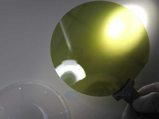
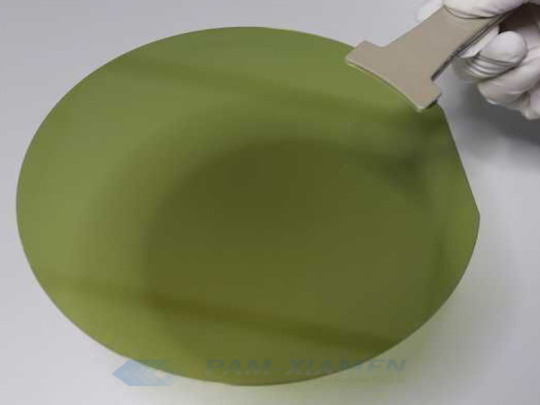
PAM XIAMEN offers GaN HEMT Epitaxial Wafers.

CZT wafer
Gallium Nitride (GaN) epitaxial wafers (epi-wafers). GaN high-electron-mobility transistors (HEMT) wafers on different substrates such as silicon essence, blue substrate, silicon carbide (SiC) substrate.
CZT wafer
We offer straight from the factory, along with therefore can offer the most effective prices on the industry for good quality GaN HEMT epi-wafers. Consumers from just about all over the world have got trustworthy PAM XIAMEN Products being a preferred supplier connected with GaN epi-wafers and GaN diffusion.
AlGaN/GaN HEMT upon only two in Conductive Semblable Wafer (GaN/SiC)
AlGaN/GaN HEMT in 2 in Blue Wafer
AlGaN/GaN HEMT about 3 inch Semi-Insulating Pareil Wafer (GaN/SiC)
AlGaN/GaN HEMT with 2 inch Mais Wafer (GaN/Si)
For a lot more information, please visit internet site: https://www.powerwaywafer.com,
send us e mail at sales@powerwaywafer. com in addition to powerwaymaterial@gmail. com
Found inside 1990, Xiamen Powerway Innovative Substance Co., Ltd (PAM-XIAMEN) is actually a leading manufacturer associated with semiconductor material in The far east. PAM-XIAMEN develops advanced ravenscroft progress and epitaxy technological innovation, making processes, engineered substrates as well as semiconductor devices. PAM-XIAMEN’s engineering enable higher efficiency and also lower cost developing of semiconductor wafer.
Top quality is the first top priority. PAM-XIAMEN have been ISO9001: '08, owns along with shares several modern facories which can easily provide quite a huge variety of qualified products to be able to meet diverse needs regarding our customers, each buy has to be managed by means of our rigorous top quality method. Test report will be presented to each shipment, in addition to each wafer are warrantee.
1 note
·
View note
Text
SiC Wafer Reclaim Services Market Predicted Expected to Witness a Sustainable Growth by 2030
The global SiC wafer reclaim services market is speculated to register significant growth through 2030 owing to the rapidly expanding electrification trend in the automotive sector. The growing acceptance of automated solutions in various companies will also lead to an upsurge in product demand.
For instance, in 2018, Tesla, the well-known EV pioneer, began incorporating SiC devices inside their cars. Since then, several OEMs are working on changing to a zero-emission policy through the promotion of EVs.
The proliferating trend of e-mobility and the emergence of new energy markets will have a profound impact on SiC wafer reclaim services market outlook. Companies are increasingly investing in wafer technology and are devising suitable development plans in accordance with the rising product demand. Improvement in the manufacturing process and increasing focus on the adoption of SiC products will push the market growth in the forthcoming years.
Get sample copy of this research report @ https://www.gminsights.com/request-sample/detail/5315
Based on diameter type, the 5-10 inches SiC wafer reclaim service market may depict an appreciable growth rate during the projection period. The robust trend of IoT adoption and the increasing penetration of smart devices have led to a substantial rise in the demand for 5-10 inch diameter components. Technological developments in artificial intelligence, automation, and 5G have prompted manufacturers to incline toward 5-10 inch diameter SiC wafers.
SiC fabs are switching from 15cm (6-inch) to 20cm (8-inch) wafers to minimize the high cost of creating SiC devices. Major SiC wafer producers and researchers are working on developing wafer sizes between 5-10 inches in order to improve manufacturing units per wafer.

With respect to applications, the SiC wafer reclaim services market size from optoelectronic devices segment is anticipated to grow at a CAGR of more than 10% between 2022-2030. The segment growth can be credited to the growing use of reclaimed SiC wafers in several optoelectronic devices including solar cells, optical fiber, blue lasers, telecommunications lasers, and photodiodes owing to the characteristics of the material, such as high heat resistance, quick cooling, and low dielectric loss at higher frequencies.
In terms of regional segmentation, the North America SiC wafer reclaim services market was worth over USD 150 million in 2021. The expansion of the regional SiC wafer reclaim industry will be driven by the rising number of government policies and efforts encouraging the development of optoelectronics in North American economies.
Request for customization @ https://www.gminsights.com/roc/5315
To take advantage of the upward trend in high-growth areas like electric vehicles (EVs), ADAS, energy infrastructure, and factory automation, semiconductor companies are taking charge and working on SiC capacity expansions. For instance, one of the leading American semiconductor suppliers, onsemi, announced the development of its SiC facility in Hudson, New Hampshire, in August 2022.
The emerging demand for EVs and growing requirement for automated devices across different sectors may push the market growth.
Table of Contents (ToC) of the report:
Chapter 1 Methodology & Scope
1.1 Scope and definition
1.2 Methodology & forecast parameters
1.3 COVID-19 impact
1.3.1 North America
1.3.2 Europe
1.3.3 Asia Pacific
1.3.4 LAMEA
1.4 Data Sources
1.4.1 Secondary
1.4.2 Primary
1.5 Industry Glossary
Chapter 2 Executive Summary
2.1 SiC wafer reclaim services market 360º synopsis, 2018 – 2030
2.2 Business trends
2.3 Regional trends
2.4 Diameter trends
2.5 Application trends
Browse complete Table of Contents (ToC) of this research report @ https://www.gminsights.com/toc/detail/sic-wafer-reclaim-services-market
About Global Market Insights:
Global Market Insights, Inc., headquartered in Delaware, U.S., is a global market research and consulting service provider; offering syndicated and custom research reports along with growth consulting services. Our business intelligence and industry research reports offer clients with penetrative insights and actionable market data specially designed and presented to aid strategic decision making. These exhaustive reports are designed via a proprietary research methodology and are available for key industries such as chemicals, advanced materials, technology, renewable energy and biotechnology.
Contact Us:
Contact Person: Arun Hegde
Corporate Sales, USA
Global Market Insights, Inc.
Phone: 1-302-846-7766
Toll Free: 1-888-689-0688
Email: [email protected]
#SiC Wafer Reclaim Services Market Analysis#SiC Wafer Reclaim Services Market by Type#SiC Wafer Reclaim Services Market Share#SiC Wafer Reclaim Services Market Development
0 notes
Text
II-VI Incorporated Receives Excellent Partner Awards from Sumitomo
II-VI Incorporated Receives Excellent Partner Awards from Sumitomo
II-VI Incorporated, a global supplier of silicon carbide substrates and devices, announced that it received two Excellent Partner Awards, from Sumitomo Electric Industries (SEI), and its subsidiary, Sumitomo Electric Device Innovations (SEDI), for their fiscal year 2020.
SEI and SEDI each announced their award, respectively, on September 8 and 15, 2021, in recognition of II-VI’s responsiveness and scalability, which contributed significantly to the expansion of Sumitomo’s business.
“II-VI is proud to receive these two awards from Sumitomo and would like to thank our teams for their dedication to excellence that made it possible,” said Dr. Chuck Mattera, Chief Executive Officer, II-VI Incorporated. “The awards reflect our strong partnership with Sumitomo and our ability to expand production capacity in response to their needs.”
Osamu Inoue, President and COO of Sumitomo Electric Industries, said that they are pleased to express their gratitude to II-VI for their notable contributions. They will continue to strengthen the partnership between their valued suppliers and the Sumitomo Electric Industries Group and strive to further mutually expand their business.
II-VI and Sumitomo are also collaborating to establish a vertically integrated, 150 mm wafer fabrication platform to manufacture state-of-the-art gallium nitride (GaN) on SiC high-electron-mobility transistor (HEMT) devices that will enable next-generation wireless networks. II-VI’s leadership in 150 mm compound semiconductor manufacturing, combined with SEDI’s leadership in GaN RF device technology, will allow II-VI and SEDI to drive best-in-class performance, greater scale, and competitive costs for 5G RF solutions.
0 notes
Text
SiC Power Semiconductor Market Is Booming Across the Globe | 2023
The market for SiC power semiconductor is projected to cross the USD 1,359 Mn and expand at a noteworthy CAGR of 26.3% over the forecast period of 2017-2023, reveals Market Research Future (MRFR) in a detailed study. The global SiC power semiconductor market was valued at USD 345.2 Mn in 2017.
Desirable features of SiC power devices such as higher critical electrical field, higher thermal conductivity, higher operating temperature, and higher current density allows SiC power devices to handle much power density as compared to traditional silicon counterparts. Major semiconductor companies have turned to the use of SiC as an ideal alternative which has spurred the growth of the global SiC power semiconductor market.
Rise in a number of energy efficiency projects to cater to the augmenting energy problems across the globe has induced high demand for SiC power semiconductors. The governments in multiple countries, especially in developing countries where energy crisis is an area of huge concern. SiC power devices exhibit advanced properties as compared to silicon and are utilized in solar power generation. SiC power semiconductors eliminate various issues associated with material limitations of silicon.
Enhanced power handling capacity, high thermal conductivity, and lower conduction loss properties of SiC power semiconductors have led to the expansion of the application range of these devices across various industry verticals which incites substantial growth in the global SiC power semiconductor market.
Being a relatively new technology, SiC power semiconductor market is met by certain challenges which are yet to be addressed. High cost of fabrication, expensive and bulky packaging, and complexities associated with the design and lack of expertise for the same are few impediments to the growth of the global SiC power semiconductor market.
Availability of gallium-nitride (GaN)-based power semiconductors as a substitute to SiC power semiconductors is expected to limit the growth of the global SiC power semiconductor market over the forecast period. Meanwhile, the introduction of 5G mobile communications is expected to create ample growth opportunities over the forecast period.
Get Free Sample Report @ https://www.marketresearchfuture.com/sample_request/6441
Segmentation
The global SiC power semiconductor market has been segmented based on device, wafer size, application, and end user.
By device, the global SiC power semiconductor market has been segmented into SiC discrete devices and SiC bare die devices. The SiC discrete devices segment has been further segmented into MOSFET, diode, and module.
By wafer size, the global SiC power semiconductor market has been segmented into 2-inch, 4-inch, and 6-inch and above.
By application, the global SiC power semiconductor market has been segmented into RF devices & cellular base stations, power supply & inverter, power grids, EV motors, industrial motor drives, railway traction, and others.
By end user, the global SiC power semiconductor market has been segmented into telecommunication, energy & power, automotive, industrial, electronics, and others.
Regional Outlook
North America, Europe, Asia Pacific (APAC), and the Rest of the World (RoW) are the key markets for SiC power semiconductor.
APAC is the largest market for SiC power and is expected to dominate the global market throughout the forecast period. Expansion of 4G and LTE network has resulted in the proliferation of RF and cellular base station in the region. The rise in a number of energy efficiency projects coupled with government initiatives to develop solar power in the region acts as a plus for the growth of the market. In addition, the region has attracted massive investments from major players which fosters market growth.
Europe is a significant market driven by a thriving automotive industry in the region. The automotive industry generates substantial demand for SiC semiconductors since they allow for overall cost reduction.
North America market accounts for a 25% share of the global market. Presence of significant silicon carbide manufacturers and high investment on R&D activities drives the market in North America.
Competitive Analysis
Mitsubishi Electric Corporation, STMicroelectronics NV, Cree Inc., ON Semiconductor, Infineon Technologies AG, and others are the eminent players in the global SiC power semiconductor market. The global SiC power semiconductor market is highly competitive where the growth of the vendors majorly depends on conditions such as government support, and industry development. In a bid to gain a competitive edge over the market, the market participants are focusing on R&D and expansion of product line to provide energy efficient and cost-effective components.
Table of Content:
4 Market Dynamics
4.1 Introduction 27
4.2 Drivers 28
4.2.1 Increase In Demand For SiC Power Semiconductor Due To Advantages Such As High Thermal Conductivity 28
4.2.2 Increase In Demand Of Power Electronics Modules Across Various Industry Verticals 28
4.2.3 Rise In Installation Of Solar Photovoltaic Panels For Electricity Generation 28
4.2.4 Drivers Impact Analysis 29
4.3 Restraints 29
4.3.1 Design Complexity And High Cost Of SiC MOSFET 29
4.3.2 Availability Of GaN As A Substitute For SiC 29
4.3.3 Restraints Impact Analysis 30
4.4 Opportunities 30
4.4.1 Introduction Of Fifth-Generation (5G) Mobile Communication 30
4.4.2 Rising Adoption Of Electric Vehicles 31
5 Market Factor Analysis
5.1 Supply Chain Analysis 33
5.1.1 Raw Material Suppliers 33
5.1.2 SiC Wafer/Substrate Manufacturers 33
5.1.3 System Integrators/Assemblers 34
5.1.4 Distributors/Value-Added Resellers (VARs) 34
5.1.5 End-Users 34
5.2 Porter’s Five Forces Model 35
5.2.1 Threat Of New Entrants 35
5.2.2 Bargaining Power Of Suppliers 35
5.2.3 Threat Of Substitutes 36
5.2.4 Bargaining Power Of Buyers 36
5.2.5 Intensity Of Rivalry 36
6 Market Alerts
6.1 Impact Analysis Of Emerging Technology 38
7 Global SiC Power Semiconductor Market, By Device
7.1 Overview 40
7.1.1 SiC Discrete Devices 40
7.1.1.1 MOSFET 40
7.1.1.2 Diode 40
7.1.1.3 Module 40
7.1.2 SiC Bare Die Devices 40
8 Global SiC Power Semiconductor Market, By Wafer Size
8.1 Overview 44
8.1.1 2-Inch 44
8.1.2 4-Inch 44
8.1.3 6-Inch And Above 44
Get Complete Report @ https://www.marketresearchfuture.com/reports/sic-power-semiconductor-market-6441
About Us
Market Research Future (MRFR) is an esteemed company with a reputation of serving clients across domains of information technology (IT), healthcare, and chemicals. Our analysts undertake painstaking primary and secondary research to provide a seamless report with a 360 degree perspective. Data is compared against reputed organizations, trustworthy databases, and international surveys for producing impeccable reports backed with graphical and statistical information.
We at MRFR provide syndicated and customized reports to clients as per their liking. Our consulting services are aimed at eliminating business risks and driving the bottomline margins of our clients. The hands-on experience of analysts and capability of performing astute research through interviews, surveys, and polls are a statement of our prowess. We constantly monitor the market for any fluctuations and update our reports on a regular basis.
Media Contact:
Market Research Future
Office No. 528, Amanora Chambers
Magarpatta Road, Hadapsar,
Pune - 411028
Maharashtra, India
+1 646 845 9312
Email: [email protected]
0 notes
Text
Know the Power of Silicon Carbide
In both the automotive and industrial markets the adoption of energy solutions with SiC materials is accelerating on a high level. Compared to making silicon wafers, making silicon carbide SiC wafers is a far more involved process and with the rising demand for SiC devices, companies that prepare them to have to nail down sources of SiC wafer.
This is important because for a variety of power components and devices used in renewable energy, electric vehicles, fast-charging stations, and various industrial applications the properties of SiC are very well-suited.
In terms of energy SiC offers several benefits, which is why in the development of the new power electronics, it has been and will be the focus of attention together with its cousin GaN.
Compared to typical silicon, SiC can withstand substantially higher voltages, up to ten times higher. This indicates that in high-voltage electronics applications fewer series components should be used that result in reducing complexity and system costs. You will come across the SiC wafer supplier too.
In the semiconductor industry, SiC SBDs are already replacing silicon. In specific markets, GaN could be a strong competitor. There has been a drastic reduction in recovery losses with Inverters having SBDs, resulting in improved efficiency. Several requirements need to be kept in mind by the power design, including space and weight, which play a significant role in inefficiency.
To power factor correctors (PFC) circuits and secondary side bridge rectifiers in switching mode power supplies SiC-SBDs are increasingly applied. In the portfolio of Rohm SiC-SBDs, 600V and 1,200V modules are included, with an amperage rating range from 5A to 40A.
The full quality of a semiconductor does not get exploited by the efficiency of conventional power electronics but only with a loss of about 15% of efficiency in the form of heat. The SiC semiconductor material has great potential to meet the requirements of these market trends because of its physical properties so they are used by SiC wafer manufacturer.
There is an increase in switching frequency by low switching losses and a reduction in component size is seen. With the increase in frequency, the size reduction is more or less proportional.
Follow our Facebook and Twitter for more information about our product.
8 notes
·
View notes

Text
GaN on Silicon Technology Market Growth, Trends and Forecasts 2027
GaN on Silicon Technology Market: Overview
According to a new research report pertaining to the GaN on silicon technology market, published by Transparency Market Research , the global GaN on silicon technology market is expected to surpass US$ 80 million by 2027, expanding at a CAGR of nearly 19% from 2019 to 2027. According to the report, the global Gallium nitride (GaN) on silicon technology market would continue to be influenced by a range of macroeconomic and market-specific factors during the forecast period.

Request a Sample - https://www.transparencymarketresearch.com/sample/sample.php?flag=S&rep_id=67223
Growing Popularity of GaN on Silicon Technology Driving the Global GaN on Silicon Technology Market
Gallium nitride (GaN) is considered as a next-generation power semiconductor. With a higher breakdown strength, higher switching speed, higher thermal conductivity, and lower on-resistance, power devices based on GaN significantly outperform Si-based power chips.
First-generation GaN-based power devices are likely to play a key role in the power conversion within battery chargers, smartphones, computers, servers, automotive lighting systems, and photovoltaic cells in the near future. At present, GaN is grown on a variety of substrates, including sapphire, silicon carbide (SiC), and silicon (Si).
Currently, the gallium nitride on silicon (GaN-on-Si) technology has reached a high level of maturity, which explores the next-generation GaN on silicon technology with a higher level of integration (GaN-IC) and performance. These devices are widely used in radio-frequency amplifiers, high-voltage applications, and LEDs, primarily due to their abilities to operate at a high frequency, power density, and temperature with improved efficiency and linearity.
Such innovations have greatly augmented the demand for devices with the GaN on silicon technology in various applications. In order to meet the rising demand for GaN semiconductor devices, leading players operating in the GaN on silicon technology market are utilizing economies of scale.
Consumer Electronics Segment to Account for a Leading Share of the Global GaN on Silicon Technology Market
The Gallium nitride (GaN) on silicon technology market report offers detailed segmentation of the global GaN on silicon technology market in terms of wafer size (50 mm, 100 mm, 150 mm, and 200 mm) and end-use industries (consumer electronics, IT & telecommunication, automotive, aerospace & defense, and others). The GaN on silicon technology market has also been segmented based on region (North America, Europe, Asia Pacific, Latin America, and the Middle East & Africa).
Among the end-use industries, the consumer electronics segment is expected to account for a leading share of the global Gallium nitride (GaN) on silicon technology market in 2019. This segment is anticipated to maintain its leading position in the GaN on silicon technology market during the forecast period.
The better performance characteristics of gallium nitride, which have enabled the incorporation of GaN in a wide range of LEDs and high-frequency RF devices, are likely to drive the global GaN on silicon technology market during the forecast period.
Asia Pacific to be a Highly Lucrative Region in the Global GaN on Silicon Technology Market
Asia Pacific witnesses high investments in gallium nitride products. Due to low power consumption, high temperature resistivity, high breakdown voltage, high electron mobility, and better thermal stability, GaN-based devices are considered ‘green technology’ devices.
M/A-COM Technology Solutions Inc., a leading supplier of high-performance analog, RF, microwave, millimeter wave, and photonic semiconductor products, announced having shipped more than one million GaN on silicon (GaN-on-Si) RF power devices to customers, to date, for use in communication, military, and other RF applications.
Investments by Key Players to Boost the Global Gallium nitride (GaN) on Silicon Technology Market
The GaN on Silicon Technology market report provides the profiles of leading players operating in the global GaN on silicon technology market. These include NXP Semiconductor, GaN Systems, Panasonic Corporation, Fujitsu Semiconductor, Transphorm Inc., Texas Instruments, Qorvo, Inc., OSRAM Opto Semiconductors GmbH, Infineon Technologies AG, and Cree, Inc.
In May 2019, Cree, Inc. announced its plans to invest up to US$ 1 Bn in the expansion of its silicon carbide production capacity, with the development of a state-of-the-art, automated facility for 200-mm silicon carbide fabrication.
In June 2015, Exagan, a startup innovator of the gallium nitride (GaN) semiconductor technology that enables the manufacturing of smaller and more efficient electric converters, announced to have raised EUR 5.7 Mn (US$ 6.38 Mn) in its first-round financing. These funds would be used to produce high-speed power switching devices on 200-mm wafers.
Request for covid19 Impact Analysis - https://www.transparencymarketresearch.com/sample/sample.php?flag=covid19&rep_id=67223
0 notes
Text
Silicon Wafers Market Potential Growth and Analysis Of Key Players - Forecast to 2025
Market Overview
Global Silicon Wafers Market is expected to reach USD 11,889.0 Million by 2025 at a CAGR of 3.19% during the forecast period. Market Research Future (MRFR), in its report, envelops segmentation and drivers to provide a better glimpse of the market in the coming years. Silicon wafers act as the perfect substrate material for modern semiconductors and microelectronic devices. It is used for producing microchips & chips and building ICs that are used in a wide range of electronic devices. Silicon wafers are polished, cleaned, and processed so that they can be used for different applications. The increasing demand for silicon wafers in consumer electronics, and the demand for the miniaturization of semiconductor devices are the growth factors for the global silicon wafer market. However, high manufacturing costs and design complexity are some of the few key factors that limit market growth.
Segmental Analysis
Global Silicon Wafers Market has been segmented based on Material, Type, Application, and Region.
Based on material, the market has been bifurcated into P-type and N-type. The P-type segment accounted for the larger market share valued at USD 5,519.7 million in 2019; it is expected to record a CAGR of 2.6% during the forecast period. The N-type segment was valued at USD 4,101.8 million; it is projected to register a higher CAGR of 3.9%.
Based on type, the silicon wafers market has been segmented into polished wafers, annealed wafers, epitaxial wafers, diffused wafers, and SOI wafers. These types are used as per the required functionality and the number of devices to be manufactured. The epitaxial wafers segment has dominated the market during the forecast period, followed by the polished wafer and SOI wafer segments. Epitaxial wafers are developed through the epitaxy process. In this process, an additional monocrystalline silicon layer is deposited on to the polished crystal surface of a silicon wafer. Moreover, these types of wafers are used in highly integrated semiconductor elements such as ICs, power devices, and various power applications. Polished wafers are silicon wafers that are either polished on a single side or on both sides to provide them with a reflective surface based on the requirement. These wafers have properties such as flatness and cleanliness. These types of wafers are prime wafers that are used in various components and devices such as MOS ICs, LSI analog, and others.
Get Free Sample Report @ https://www.marketresearchfuture.com/sample_request/2052
Based on application, the silicon wafers market has been segmented into solar cells, integrated circuits, photoelectric cells, smartphones, tablets, smart wafers, microchips, transistors, diodes and rectifiers, MEMS fabrication, and others. The rising development in the electronics industry is another factor that is increasing the scope of application for silicon wafers. Silicon wafers play a vital role in the overall functionality of solar cells, as silicon is the basic component for these cells. Silicon wafers are used in solar cells due to their optical, electronic, mechanical, and thermal properties. Additionally, to increase the capability of silicon in the solar cells, various impurities are imposed on the silicon wafers, which enhance the overall performance of the cells and covert the sun’s energy into electrical energy.
By wafer size, the market is segmented into 300mm, 150mm, 200mm, and 450mm and above. The 300 mm wafers are widely used for several applications. The diameter of this type of wafer is generally larger to improve throughput and reduce costs. The increasing demand for connected devices, data transport and storage, big data, and AI technology drives the market for 300mm wafers. They are widely used in semiconductor components such as commodity chips, including DRAMs, flash memory, and microprocessors owing to their high-volume. Recently, most of the image sensors, power management devices, and complex logic and micro component ICs with large die sizes have been produced on 300 mm wafers. Chipmakers such as Samsung, Toshiba, and Micron, use 300mm wafers for most of their chip production.
The global silicon wafers market, by region, has been segmented into North America, Europe, Asia-Pacific, and the rest of the world. Asia-Pacific accounted for the largest market share with a market value of USD 4,371.2 million in 2019. North America was the second-largest market in 2019, valued at USD 2,383.0 million.
Competitive Analysis
The Key Players of the Global Silicon Wafers Market are Shin-Etsu Chemical Co., Ltd. (Japan), SK Siltron Co., Ltd. (South Korea), Siltronic AG (Germany), GlobalWafers Co., Ltd. (Taiwan), Wafer World, Inc. (US), Advanced Semiconductor, Inc. (US), Sumco Corporation (Japan), Soitec SA (France), Silicon Materials, Inc. (US), Addison Engineering, Inc. (US), and Virginia Semiconductor, Inc. (US), among others.
In March 2020, SK Siltron completed the acquisition of DuPont's silicon carbide wafer (SiC wafer) unit. This acquisition will help fulfill the demand from consumers and governments for sustainable energy and environmental solutions.
In September 2019, Soitec SA announced increasing its production capacity for its piezoelectric-on-insulator (POI) substrate to meet the growing demand. The POI substrate is used in 4G/5G surface acoustic wave (SAW) filters, offers built-in temperature compensation, and allows the integration of multiple filters on a single die.
In February 2019, Soitec SA and Simgui announced the enhancement of their partnership and increased the production capacity of 200mm SOI wafers in China, for future growth.
Table of Content:
3 RESEARCH METHODOLOGY
4 MARKET DYNAMICS
4.1 OVERVIEW
4.2 DRIVERS
4.2.1 INCREASING DEMAND FOR SILICON WAFERS IN CONSUMER ELECTRONICS
4.2.2 DEMAND FOR MINIATURIZATION OF SEMICONDUCTOR DEVICES
4.2.3 DRIVERS IMPACT ANALYSIS
4.3 RESTRAINTS
4.3.1 HIGH MANUFACTURING COSTS
4.3.2 DESIGN COMPLEXITY
4.4 OPPORTUNITIES
4.4.1 TECHNOLOGICAL ADVANCEMENTS IN CONSUMER ELECTRONICS
4.5 ECONOMIC IMPACT ON OVERALL MANUFACTURING INDUSTRY
4.6 IMPACT ON SILICON WAFER MARKET
4.6.1 IMPACT ON SUPPLY CHAIN
4.6.2 PRICE VARIATION OF KEY RAW MATERIALS
4.6.3 PRODUCTION SHUTDOWN
4.6.4 IMPACT ON MARKET DEMAND
5 MARKET FACTOR ANALYSIS
5.1 VALUE CHAIN ANALYSIS
5.1.1 RESEARCH AND DEVELOPMENT
5.1.2 MATERIAL SUPPLIERS AND FOUNDRIES
5.1.3 WAFER MANUFACTURERS
5.2 PORTER’S FIVE FORCES MODEL
5.2.1 THREAT OF NEW ENTRANTS
5.2.2 BARGAINING POWER OF SUPPLIERS
5.2.3 BARGAINING POWER OF BUYERS
5.2.4 THREAT OF SUBSTITUTES
5.2.5 RIVALRY
6 GLOBAL SILICON WAFER MARKET, BY MATERIAL
6.1 OVERVIEW
6.2 N-TYPE
6.3 P-TYPE
7 GLOBAL SILICON WAFER MARKET, BY TYPE
7.1 OVERVIEW
7.2 POLISHED WAFER
7.3 ANNEALED WAFER
7.4 EPITAXIAL WAFER
7.5 DIFFUSED WAFER
7.6 SOI WAFER
Get Complete Report @ https://www.marketresearchfuture.com/reports/silicon-wafers-market-2052
About Us
Market Research Future (MRFR) is an esteemed company with a reputation of serving clients across domains of information technology (IT), healthcare, and chemicals. Our analysts undertake painstaking primary and secondary research to provide a seamless report with a 360 degree perspective. Data is compared against reputed organizations, trustworthy databases, and international surveys for producing impeccable reports backed with graphical and statistical information.
We at MRFR provide syndicated and customized reports to clients as per their liking. Our consulting services are aimed at eliminating business risks and driving the bottomline margins of our clients. The hands-on experience of analysts and capability of performing astute research through interviews, surveys, and polls are a statement of our prowess. We constantly monitor the market for any fluctuations and update our reports on a regular basis.
Media Contact:
Market Research Future
Office No. 528, Amanora Chambers
Magarpatta Road, Hadapsar,
Pune - 411028
Maharashtra, India
+1 646 845 9312
Email: [email protected]
0 notes
Text
Global Silicon Carbide Power Semiconductors Market is Projected to Reach $1,109 million by 2025
The global silicon carbide (SiC) power semiconductor market was valued at $302 million in 2017, and is projected to reach $1,109 million by 2025, registering a CAGR of 18.1% from 2018 to 2025. The Asia-Pacific captured the highest market share of 49% in 2017 and is expected to be dominant throughout the forecast period, that is, 2018 to 2025.

Silicon carbide (SiC) power semiconductor is a compound semiconductor formed by combining silicon and carbide. It is majorly used in power electronics systems, which deal with control and conversion of electrical power effectively and efficiently. Silicon carbide (SiC) power devices have evolved from immature prototypes in laboratories to viable alternatives to Si-based power devices in high-efficiency and high-power density applications, owing to rapid innovation and development of the semiconductors industry.
Request for Sample @ https://www.kdmarketinsights.com/sample/4234
SiC-based power devices have significant advantages over silicon-based power devices such as high breakdown voltage, high operating electric field, high operating temperature, high switching frequency, and low losses. SiC-based semiconductors are applicable in areas where high temperature, high voltage, and high-power density are required.
Increasing number of high-voltage, high-efficiency, and high-power density applications, such as industrial motor drives, telecommunication, renewable energy systems, and automotive electronics, drives the growth of the silicon carbide power semiconductors market. Moreover, there is increased penetration of electric vehicles, owing to government support and initiatives. Thus, increasing usage of SiC power devices in automotive electronics drives the market.
However, the growth of the SiC power semiconductors market is restrained by the high wafer cost of silicon carbide. High-purity SiC powder and high-purity silane (SiH4) are the critical precursors for producing SiC layers in the chips. High-purity SiC powder is currently available from a limited number of suppliers and is relatively expensive, while high-purity silane is produced by a few large multinational industrial gas companies. Thus, the market is restrained by the fewer raw material suppliers required for the creation of SiC substrates. However, owing to the rising technological developments, such as the advent of 5G, lucrative opportunities are created for the growth of the silicon carbide power semiconductors market.
The global silicon carbide (SiC) power semiconductors market is segmented by power module, industry vertical, and region. According to power module, it is bifurcated into power product and discrete product. On the basis of industry vertical, it is categorized into IT & telecom, aerospace & defense, industrial, energy & power, electronics, automotive, and healthcare. Based on region, it is analyzed across North America, Europe, Asia-Pacific, and LAMEA.
Key Benefits for Silicon Carbide Power Semiconductors Market:
- This study comprises the analytical depiction of the global silicon carbide power semiconductors market along with the current trends and future estimations to depict the imminent investment pockets.
- The overall market potential is determined to understand the profitable trends to gain a stronger coverage in the market.
- The report presents information related to key drivers, restraints, and opportunities with a detailed impact analysis.
- The current market is quantitatively analyzed from 2018 to 2025 to highlight the financial competency of the market.
- Porter's Five Forces analysis illustrates the potency of the buyers and suppliers.
Silicon Carbide Power Semiconductors Key Market Segments:
By Power Module
- Power product
- Discrete product
By Industry Vertical
- IT & telecom
- Aerospace & defense
- Industrial
- Energy & power
- Electronics
- Automotive
- Healthcare
By Region
North America
- U.S.
- Canada
- Mexico
Europe
- UK
- Germany
- France
- Italy
- Rest of Europe
Asia-Pacific
- China
- India
- Japan
- Australia
- South Korea
- Rest of Asia-Pacific
LAMEA
- Brazil
- Saudi Arabia
- South Africa
- Rest of LAMEA
Browse Full Report With TOC@ https://www.kdmarketinsights.com/product/silicon-carbide-power-semiconductors-market-amrr
Table of Contents@
CHAPTER 1: INTRODUCTION
1.1. REPORT DESCRIPTION
1.2. KEY BENEFITS FOR STAKEHOLDERS
1.3. KEY MARKET SEGMENTS
1.4. RESEARCH METHODOLOGY
1.4.1. Primary research
1.4.2. Secondary research
1.4.3. Analyst tools and models
CHAPTER 2: EXECUTIVE SUMMARY
2.1. CXO PERSPECTIVE
CHAPTER 3: MARKET OVERVIEW
3.1. MARKET DEFINITION AND SCOPE
3.2. KEY FINDINGS
3.2.1. Top impacting factors
3.2.2. Top investment pockets
3.2.3. Top winning strategies
3.3. PORTERS FIVE FORCES ANALYSIS
3.3.1. Moderate to high bargaining power of suppliers
3.3.2. Moderate threat of new entrants
3.3.3. Moderate threat of substitutes
3.3.4. Moderate to high intensity of rivalry
3.3.5. Moderate to high bargaining power of buyers
3.4. KEY PLAYER POSITIONING, 2017 (%)
3.5. MARKET DYNAMICS
3.5.1. Drivers
3.5.1.1. Advantages of compound semiconductors (SiC) over silicon-based technology.
3.5.1.2. Increase in demand of power electronics modules across various industry verticals.
3.5.1.3. Rise in installation of solar photovoltaic panels for electricity generation.
3.5.1.4. Growth in demand of electric vehicles, plug-in electric vehicles, and hybrid electric vehicles.
3.5.2. Restraints
3.5.2.1. High wafer cost of silicon carbide semiconductors.
3.5.2.2. Complexity in supply chain and designing process of SiC semiconductor technology.
3.5.3. Opportunities
3.5.3.1. Advent of 5G mobile communication.
CHAPTER 4: SILICON CARBIDE (SIC) POWER SEMICONDUCTORS MARKET, BY POWER MODULE
4.1. OVERVIEW
4.2. POWER PRODUCTS
4.2.1. Key market trends, growth factors, and opportunities
4.2.2. Market size and forecast, by region
4.2.3. Market analysis, by country
4.3. DISCRETE PRODUCTS
4.3.1. Key market trends, growth factors, and opportunities
4.3.2. Market size and forecast, by region
4.3.3. Market analysis, by country
CHAPTER 5: SILICON CARBIDE (SIC) POWER SEMICONDUCTORS MARKET, BY INDUSTRY VERTICAL
5.1. OVERVIEW
5.2. IT & TELECOM
5.2.1. Key market trends, growth factors, and opportunities
5.2.2. Market size and forecast, by region
5.2.3. Market analysis, by country
5.3. AEROSPACE & DEFENSE
5.3.1. Key market trends, growth factors, and opportunities
5.3.2. Market size and forecast, by region
5.3.3. Market analysis, by country
5.4. INDUSTRIAL
5.4.1. Key market trends, growth factors, and opportunities
5.4.2. Market size and forecast, by region
5.4.3. Market analysis, by country
5.5. ENERGY & POWER
5.5.1. Key market trends, growth factors, and opportunities
5.5.2. Market size and forecast, by region
5.5.3. Market analysis, by country
5.6. ELECTRONICS
5.6.1. Key market trends, growth factors, and opportunities
5.6.2. Market size and forecast, by region
5.6.3. Market analysis, by country
5.7. AUTOMOTIVE
5.7.1. Key market trends, growth factors, and opportunities
5.7.2. Market size and forecast, by region
5.7.3. Market analysis, by country
5.8. HEALTHCARE
5.8.1. Key market trends, growth factors, and opportunities
5.8.2. Market size and forecast, by region
5.8.3. Market analysis, by country
Continue…
Check for Discount@ https://www.kdmarketinsights.com/discount/4234
About KD Market Insights
KD Market Insights has come with the idea of helping business by intelligent decision making and thorough understanding of the industry. We offer a comprehensive database of syndicated research, customized reports as well as consulting services to help a business grow in their respective domain. At KD Market Insights, we offer our client a deep Market research reports accompanied by business consulting services that can help them to reach on top of the corporate world. Our customized reports are built by keeping all factors of the industry in mind.
Contact Us
150 State street, 3rd Floor,
Albany, New York
United states (12207)
Telephone: +1-518-300-1215
Email: - [email protected]
Website: - www.kdmarketinsights.com
#Silicon Carbide Power Semiconductors Market#Silicon Carbide Power Semiconductors Market Size#Silicon Carbide Power Semiconductors Market Share#Silicon Carbide Power Semiconductors Market Growth
0 notes
Text
Sapphire Wafer Market Trends, Regulations and Competitive Landscape Outlook to 2025
4 February 2019 - The Global Sapphire Wafer Market is expected to display incessant growth in forthcoming periods. With intense competition between niche players in the sapphire wafer market, the market appears to be highly fragmented and this competition is most likely to prolong over the forecast period. The market for sapphire substrates is expected to witness immense growth in forecast period because of a growing market for substrates and this growth is being augmented by LED lights and screens.

Asia pacific is on the verge of growth in sapphire wafer market with a confluence of players and right mix of raw materials and equipment suppliers together with cheap cost of labor that has fired markets accelerating market growth. North America is experiencing growth in markets on account of application of semiconductors in Radio frequency Integrated Circuits (RFIC) and laser diodes thus giving into growth of industry.
View Full Report with TOC @ https://www.millioninsights.com/industry-reports/sapphire-wafer-market
Lately, silicon-on-substrate technology has added momentum to sapphire wafer by its enhanced insulating properties that reinforce the SOS technology, thus reverberating growth in sapphire wafer industry. A distinct advantage is the imminent use of LED’s in various industries that is fueling growth of sapphire wafer market. With a growth in electronics industry, the sapphire wafer market is exhibiting abundant signs of growth fostered by low price of sapphire and excellent properties.
Overestimating demand of sapphire ingots given its very high properties had markets slightly inundated with manufacturers overstepping growth due to which the sapphire wafer market may be slightly hampered. Furthermore signifying entry of GaN-on-Si based LED in the market, sapphire wafer industry is expected to be hampered during forecast period. Though LED’s have etched a strong market in sapphire wafers substrates, the markets are becoming stronger with home buttons of smart phones, Apple watches, lens covers and digital cameras strongly expressing market growth.
Segmentation of sapphire wafer market by diameter includes 2 inches, 4 inches, 6 incches and others. Segmentation of sapphire wafer industry by technologies includes KY, CZ, HEM and EFG. Segmentation of the market by substrate wafer includes SI-on-Sapphire, SiC-on-Sapphire, GaN-on-Sapphire and others. Segmentation of sapphire market by applications includes light emitting diode (LED), Radio Frequency Integrated Circuits (RFIC), Laser Diodes , Silcicon on sapphire (SoS) IC’s and others.
By geographical region, segmentation includes North America, Europe, Asia Pacific, MEA and Latin America. The key industrial players in the sapphire wafer market include Crystal Applied Technology, Hansol Technics Co. Ltd., Mono crystal, Teraxytal Technology Corp, Rubicon Technology and Crystaland.
Market Segment:
Geographically, this report is segmented into several key Regions, with production, consumption, revenue (million USD), market share and growth rate of Sapphire Wafer in these regions, from 2013 to 2025 (forecast), covering
• North America
• Europe
• China
• Japan
• Southeast Asia
• India
Global Sapphire Wafer market competition by top manufacturers, with production, price, revenue (value) and market share for each manufacturer; the top players including
• Crystal Applied Technology Inc.
• Crystalwise Technology Inc.
• DK Aztec Co. Ltd.
• Gavish
• Guangdong Saifei Sapphire Technology Co., Ltd.
• Guizhou Haotian Optoelectronics Technology Co. Ltd.
• Hansol Technics Co. Ltd.
• Hua Shun Technology Co., Ltd.
• ILJIN Display Co. Ltd.
Request Sample Copy of This Report @ https://www.millioninsights.com/industry-reports/sapphire-wafer-market/request-sample
#Sapphire Wafer Market Trend#Sapphire Wafer Market Share#Sapphire Wafer Market Growth#Sapphire Wafer Market Segment#Sapphire Wafer Market Forecast
0 notes
Text
GaN Semiconductor Devices Market 2020 - 2027: Global Segments, Emerging Audience, Regional Study, Size, Industry Profit Growth and Business Trends
GaN Semiconductor Devices Market: Introduction
Transparency Market Research delivers key insights on the global GaN semiconductor devices market. In terms of revenue, the global GaN semiconductor devices market is estimated to expand at a CAGR of 14.5% during the forecast period, owing to numerous factors, regarding which TMR offers thorough insights and forecasts in its report on the global GaN semiconductor devices market.
Gallium nitride (GaN), a wide band gap semiconductor material, is a newer technology compared to other semiconductor materials, such as gallium arsenide (GaAs) and silicon carbide (SiC). GaN semiconductor devices offer a competitive advantage in terms of thermal performance, efficiency, weight, and size. GaN is the next-generation power semiconductor and hence, different countries are involved in developing widespread applications of GaN semiconductors. The wide band gap (WBG) semiconductor technology has matured rapidly over the last few years. Based on product, the global GaN semiconductor devices market has been classified into power semiconductors, radio devices, and opto semiconductors. Among these, opto semiconductors are being adopted largely, as they absorb and emit light. Photodiodes, LEDs, solar cells, and semiconductor lasers are all categorized as opto semiconductors. Furthermore, based on end-use industry, the global GaN semiconductor devices market has been classified into information & communication technology, automotive, consumer electronics, aerospace & defense, and others. The consumer electronics sector is increasingly adopting GaN semiconductor devices, as GaN is widely incorporated into radio frequency devices, light-emitting diodes (LEDs), and power electronics, due to its ability to operate at a high frequency and high temperature. This, in turn, is expected to boost the global GaN semiconductor devices market during the forecast period.
For More Info | Download PDF Brochure, Click Here: https://www.transparencymarketresearch.com/sample/sample.php?flag=B&rep_id=1034
GaN Semiconductor Devices Market: Dynamics
Improved responsiveness and enhanced battlefield performance are important areas of focus for the defense sector. Hence, a high level of integration is required between radar communication systems and electronic warfare devices that are used in military. Due to high breakdown voltage and rapid heat dissipation capacity, GaN semiconductor devices have benefitted the defense industry greatly. A major application of GaN in the military sector is its usage in HEMTs (high electron mobility transistors), which are required for high-frequency operations. Furthermore, due to high temperature resistivity, low power consumption, high breakdown voltage, better thermal stability, and high electron mobility, GaN semiconductor devices are widely acknowledged as ‘green technology’ by different industrial sectors. These devices are largely used in light-emitting diodes (LEDs), radio frequency (RF) amplifiers, and power electronics, due to their unique properties. With rapid advancements in technology, usage of GaN is expected to be extended to various other commercial applications. Additionally, advancements intended to increase wafer diameters are expected to improve the efficiency and reduce the cost of GaN devices, eventually improving the performance of these devices and making GaN more acceptable compared to other semiconductor materials. These are expected to be prominent factors propelling the global GaN semiconductor devices market during the forecast period.
GaN Semiconductor Devices Market: Prominent Regions
Asia Pacific is a dominant region of the global GaN semiconductor devices market. Growth of the market in the region can be attributed to presence of a large number of GaN raw material suppliers in the region. A majority of market players in this region are located in Japan, South Korea, and China. The lower production and labor costs in these countries are aiding manufacturers to set up their production facilities. Additionally, the GaN semiconductor devices market in Asia Pacific is primarily driven by the increasing demand from the consumer electronics sector, most importantly from mobile, communication, and computing segments of the sector. The electronics industry in countries such as China and India is expanding at a rapid pace. Hence, these countries are expected to be potential markets for GaN semiconductor devices in the near future. In addition, China is planning to adopt LED and solid-state lighting technologies as well as radio frequency devices in the next few years. Thus, owing to growing economy and significant availability of skilled labor and raw materials, several companies are looking forward to shifting their manufacturing units to Asia Pacific. Considering all the above-mentioned factors, the GaN semiconductor devices market in Asia Pacific is expected to witness steady growth between 2019 and 2027. The market in North America and Europe is estimated to witness significant growth during the forecast period, due to wide utilization of GaN-based transistors in defense & military and consumer electronics sectors in these regions. The GaN semiconductor devices market in Middle East & Africa and South America is expected to witness moderate growth in the near future.
Request For Covid19 Impact Analysis Across Industries And Markets – https://www.transparencymarketresearch.com/sample/sample.php?flag=covid19&rep_id=1034
GaN Semiconductor Devices Market: Key Players
Key players operating in the global GaN semiconductor devices market are Cree, Inc., Efficient Power Conversion Corporation, FUJITSU, GaN Systems, NICHIA CORPORATION, NXP Semiconductors, Renesas Electronics Corporation, Toshiba Corporation, Texas Instruments Incorporated, and Transphorm Inc.
Global GaN Semiconductor Devices Market: Segmentation
GaN Semiconductor Devices Market, by Product
Power Semiconductors
Radio Devices
Opto Semiconductors
GaN Semiconductor Devices Market, by Component
Diodes
Transistors
Integrated Circuits (ICs)
Others
GaN Semiconductor Devices Market, by Wafer Size
2 Inch
4 Inch
6 Inch
8 Inch
GaN Semiconductor Devices Market, by End-use Industry
Information & Communication Technology
Automotive
Consumer Electronics
Aerospace & Defense
Others
GaN Semiconductor Devices Market, by Region
North America
Europe
Asia Pacific (APAC)
Middle East & Africa (MEA)
South America
U.S.
Canada
Rest of North America
U.K.
Italy
Germany
France
Rest of Europe
Japan
China
India
Rest of APAC
GCC Countries
South Africa
Rest of MEA
Brazil
Rest of South America
Customization of the Report: This report can be customized as per your needs for additional data or countries. – https://www.transparencymarketresearch.com/sample/sample.php?flag=CR&rep_id=1034
Related Reports Press-Release –
https://www.prnewswire.com/news-releases/anti-microbial-and-stain-free-design-of-period-panties-menstrual-underwear-to-inundate-market-growth-noted-tmr-300870237.html
https://www.prnewswire.com/news-releases/cognitive-computing-market-to-expand-at-phenomenal-rate-of-cagr-49-9-cloud-applications-to-promote-growth—tmr-300845175.html
About Us
Transparency Market Research (TMR) is a market intelligence company, providing global business information reports and services. Our exclusive blend of quantitative forecasting and trends analysis provides forward-looking insight for thousands of decision makers. TMR’s experienced team of Analysts, Researchers, and Consultants, use proprietary data sources and various tools and techniques to gather, and analyze information. Our business offerings represent the latest and the most reliable information indispensable for businesses to sustain a competitive edge.
Each TMR syndicated research report covers a different sector – such as heavy engineering equipment, pharmaceuticals, chemicals, energy, food & beverages, semiconductors, med-devices, consumer goods and technology. These reports provide in-depth analysis and deep segmentation to possible micro levels. With wider scope and stratified research methodology, TMR’s syndicated reports thrive to provide clients to serve their overall research requirement.
US Office Contact
90 State Street, Suite 700
Albany, NY 12207
Tel: +1-518-618-1030
USA – Canada Toll Free: 866-552-3453
Email: [email protected]
Website: https://www.transparencymarketresearch.com
0 notes
Text
Bespoke Items
Welcome to Thermic Edge.
We are an independent supplier of Heater Stage systemsto many industries and research institutions. To meet the ever growing demand for Substrate Heating within numerous industrial and research areas, Thermic Edge has continually re-invested and trained a team of expert Design Engineers to aid the customer in the development of a Heater Stage system which meets thei requirements.
To this end, Thermic Edge are expert in providing bespoke, one of a kind, Sample Heater systems including but not limited to:
Laboratory Vacuum Furnaces
UHV Heaters
Heater Stages

• Small form Button Heaters

Thermic Edge have developed a tried and tested approach to the design of bespoke systems for the end user. This combined with in depth knowledge of the Vacuum Heating industry has allowed us to ensure that customer requirements are met to the highest standard.
When a customer sends through an enquiry, it is immediately entered into our system and our team of technical sales staff will aid the customer in the identification and quotation of a suitable system. Where Thermic Edge differ from many companies is that the Sales and Customer liaisons within the company all come from a technical background and have hands on experience both designing and building all products from Heater Stages, through to Laboratory Vacuum Furnaces.
When the customer places an order, they are assigned a Design Engineer who will be their personal Engineer for the design process. Thermic Edge pride themselves on the ability to quickly and with clarity, aid the customer in design changes,and implementation of their system. The Design Engineer will work directly with the customer to ensure that all objectives of the order are met.
Bespoke orders are not just limited to Heater Stages and Vacuum Furnaces. Thermic Edge owns and operates a SiC Coating facility in Scotland which produces a High Purity Silicon Carbide Coating. This means that Thermic Edge are able to offer bespoke items both one offs and batch quantities for Silicon Carbide Coated Graphite. This includes, but is not limited to SiC Coated Susceptors, SiC Coated Wafer Holders, SiC Coating for MoCVD, and SiC Coated Elements
The SiC Coated Graphite Components offered by Thermic Edge can meet any number of customer requirements, shapes and sizes. Our in-house team of Design Engineers will take the customers design and translate it in house to ensure that the coating does not affect the overall geometry or functionality of the finished piece.
To learn more about our in-house services for custom components, contact us at any time and one of our team will be in contact.
0 notes
Text
GaN Semiconductor Devices Market - Anticipated To Witness High Growth In The Near Future
GaN Semiconductor Devices Market: Introduction
Transparency Market Research delivers key insights on the global GaN semiconductor devices market. In terms of revenue, the global GaN semiconductor devices market is estimated to expand at a CAGR of 14.5% during the forecast period, owing to numerous factors, regarding which TMR offers thorough insights and forecasts in its report on the global GaN semiconductor devices market.
Gallium nitride (GaN), a wide band gap semiconductor material, is a newer technology compared to other semiconductor materials, such as gallium arsenide (GaAs) and silicon carbide (SiC). GaN semiconductor devices offer a competitive advantage in terms of thermal performance, efficiency, weight, and size. GaN is the next-generation power semiconductor and hence, different countries are involved in developing widespread applications of GaN semiconductors. The wide band gap (WBG) semiconductor technology has matured rapidly over the last few years. Based on product, the global GaN semiconductor devices market has been classified into power semiconductors, radio devices, and opto semiconductors. Among these, opto semiconductors are being adopted largely, as they absorb and emit light. Photodiodes, LEDs, solar cells, and semiconductor lasers are all categorized as opto semiconductors. Furthermore, based on end-use industry, the global GaN semiconductor devices market has been classified into information & communication technology, automotive, consumer electronics, aerospace & defense, and others. The consumer electronics sector is increasingly adopting GaN semiconductor devices, as GaN is widely incorporated into radio frequency devices, light-emitting diodes (LEDs), and power electronics, due to its ability to operate at a high frequency and high temperature. This, in turn, is expected to boost the global GaN semiconductor devices market during the forecast period.
Request A Sample Copy Of The Report https://www.transparencymarketresearch.com/sample/sample.php?flag=S&rep_id=1034
GaN Semiconductor Devices Market: Dynamics
Improved responsiveness and enhanced battlefield performance are important areas of focus for the defense sector. Hence, a high level of integration is required between radar communication systems and electronic warfare devices that are used in military. Due to high breakdown voltage and rapid heat dissipation capacity, GaN semiconductor devices have benefitted the defense industry greatly. A major application of GaN in the military sector is its usage in HEMTs (high electron mobility transistors), which are required for high-frequency operations. Furthermore, due to high temperature resistivity, low power consumption, high breakdown voltage, better thermal stability, and high electron mobility, GaN semiconductor devices are widely acknowledged as ‘green technology’ by different industrial sectors. These devices are largely used in light-emitting diodes (LEDs), radio frequency (RF) amplifiers, and power electronics, due to their unique properties. With rapid advancements in technology, usage of GaN is expected to be extended to various other commercial applications. Additionally, advancements intended to increase wafer diameters are expected to improve the efficiency and reduce the cost of GaN devices, eventually improving the performance of these devices and making GaN more acceptable compared to other semiconductor materials. These are expected to be prominent factors propelling the global GaN semiconductor devices market during the forecast period.
GaN Semiconductor Devices Market: Prominent Regions
Asia Pacific is a dominant region of the global GaN semiconductor devices market. Growth of the market in the region can be attributed to presence of a large number of GaN raw material suppliers in the region. A majority of market players in this region are located in Japan, South Korea, and China. The lower production and labor costs in these countries are aiding manufacturers to set up their production facilities. Additionally, the GaN semiconductor devices market in Asia Pacific is primarily driven by the increasing demand from the consumer electronics sector, most importantly from mobile, communication, and computing segments of the sector. The electronics industry in countries such as China and India is expanding at a rapid pace. Hence, these countries are expected to be potential markets for GaN semiconductor devices in the near future. In addition, China is planning to adopt LED and solid-state lighting technologies as well as radio frequency devices in the next few years. Thus, owing to growing economy and significant availability of skilled labor and raw materials, several companies are looking forward to shifting their manufacturing units to Asia Pacific. Considering all the above-mentioned factors, the GaN semiconductor devices market in Asia Pacific is expected to witness steady growth between 2019 and 2027. The market in North America and Europe is estimated to witness significant growth during the forecast period, due to wide utilization of GaN-based transistors in defense & military and consumer electronics sectors in these regions. The GaN semiconductor devices market in Middle East & Africa and South America is expected to witness moderate growth in the near future.
Request For Covid19 Impact Analysis https://www.transparencymarketresearch.com/sample/sample.php?flag=covid19&rep_id=1034
GaN Semiconductor Devices Market: Key Players
Key players operating in the global GaN semiconductor devices market are Cree, Inc., Efficient Power Conversion Corporation, FUJITSU, GaN Systems, NICHIA CORPORATION, NXP Semiconductors, Renesas Electronics Corporation, Toshiba Corporation, Texas Instruments Incorporated, and Transphorm Inc.
Global GaN Semiconductor Devices Market: Segmentation
GaN Semiconductor Devices Market, by Product
Power Semiconductors
Radio Devices
Opto Semiconductors
GaN Semiconductor Devices Market, by Component
Diodes
Transistors
Integrated Circuits (ICs)
Others
GaN Semiconductor Devices Market, by Wafer Size
2 Inch
4 Inch
6 Inch
8 Inch
GaN Semiconductor Devices Market, by End-use Industry
Information & Communication Technology
Automotive
Consumer Electronics
Aerospace & Defense
Others
GaN Semiconductor Devices Market, by Region
U.S.
Canada
Rest of North America
U.K.
Italy
Germany
France
Rest of Europe
Japan
China
India
Rest of APAC
GCC Countries
South Africa
Rest of MEA
Brazil
Rest of South America
Related Reports Press-Release –
https://www.prnewswire.com/news-releases/sake-brewery-industry-to-play-a-positive-role-in-cubitainers-market-growth-from-2020-to-2028-transparency-market-research-301104740.html
Related Reports Press-Release –
https://www.prnewswire.com/news-releases/penetration-of-advanced-technologies-to-bring-a-paradigm-shift-in-growth-of-warranty-management-system-market-north-america-to-add-numerous-feathers-of-growth-opines-tmr-301110185.html
About Us
Transparency Market Research (TMR) is a market intelligence company, providing global business information reports and services. Our exclusive blend of quantitative forecasting and trends analysis provides forward-looking insight for thousands of decision makers. TMR’s experienced team of Analysts, Researchers, and Consultants, use proprietary data sources and various tools and techniques to gather, and analyze information. Our business offerings represent the latest and the most reliable information indispensable for businesses to sustain a competitive edge.
Each TMR syndicated research report covers a different sector - such as heavy engineering equipment, pharmaceuticals, chemicals, energy, food & beverages, semiconductors, med-devices, consumer goods and technology. These reports provide in-depth analysis and deep segmentation to possible micro levels. With wider scope and stratified research methodology, TMR’s syndicated reports thrive to provide clients to serve their overall research requirement.
US Office Contact
90 State Street, Suite 700
Albany, NY 12207
Tel: +1-518-618-1030
USA - Canada Toll Free: 866-552-3453
Email: [email protected]
Website: https://www.transparencymarketresearch.com
0 notes
Last Seen Blogs

rainbow--pastel
Rainbow Pastel

musicistheair-blog
Music Is The Air

cuevana3-blue-beetle-latino
Cuevana3 —Ver Blue Beetle 2023 Gratis en Español Latino Onlin

cherubcow
Cherub Cow

porticlecraft
PorticleCraft