#spi flash programmer software
Explore tagged Tumblr posts
Visit Tumblr Blog
Explore Tumblr blogs with no restrictions, modern design and the best experience.
Last Seen Tumblr Blogs


Fun Fact
China blocked Tumblr because of pornography and censorship problems in 2013.
Text
https://www.futureelectronics.com/p/semiconductors--memory--flash--norflash--serial/s25fl256sagnfi001-infineon-7056191
USB flash memory storage, spi flash programmer software, memory chip
FL-S Series 256 Mb (32 M x 8) 3.6V 133MHz Non-Volatile SPI Flash Memory - WSON-8
#NOR Flash Memory#Serial NOR Flash (SPI) Memory#S25FL256SAGNFI001#Infineon#Memory ICs#Flash Memory#applications#USB flash memory storage#spi flash programmer software#memory chip#spi flash programmer#Memory Storage
1 note
·
View note
Text
A Comprehensive Guide to Firmware Development

In the world of embedded systems and smart devices, firmware plays a critical role in enabling hardware to function effectively. Whether you're developing IoT devices, automotive systems, or industrial machinery, firmware development is the backbone that bridges hardware and software.
In this blog post, we’ll explore what firmware is, its importance, the development process, tools used, and best practices to ensure efficient and secure firmware solutions.
What is Firmware?
Firmware is a specialized type of software that provides low-level control for a device's specific hardware. Unlike regular software applications, firmware is tightly coupled with the hardware and is often stored in non-volatile memory such as ROM, EEPROM, or flash memory.
Examples of devices with firmware include:
Smartphones
Routers
Smart TVs
Medical devices
Automotive control units (ECUs)
Why is Firmware Important?
Firmware is essential because it:
Controls hardware operations: Without firmware, the hardware components of a device would be non-functional.
Ensures device functionality: It manages startup routines, I/O operations, sensor integration, and communication protocols.
Supports software-hardware integration: Firmware acts as a middle layer, allowing high-level software applications to interact with low-level hardware components.
Enables updates: Firmware can often be updated to fix bugs, enhance performance, or add features.
The Firmware Development Process
1. Requirements Gathering
Understanding the hardware specifications and the device’s purpose is crucial. Developers need to gather requirements from both hardware engineers and end users.
2. Architecture Design
This involves deciding on the architecture and communication protocols (e.g., I2C, SPI, UART), memory usage, and timing constraints.
3. Choosing a Development Platform
Most firmware is written in C or C++ due to their efficiency and hardware-level access. You’ll also need:
Microcontroller/microprocessor datasheets
Board Support Packages (BSPs)
RTOS (Real-Time Operating System), if required
4. Coding and Integration
Firmware code is written to interface directly with hardware. This includes writing drivers for peripherals (LEDs, sensors, motors) and managing power consumption, timing, and interrupts.
5. Testing and Debugging
Testing includes:
Unit testing
Hardware-in-the-loop (HIL) testing
Simulation and emulation tools
Debugging tools such as JTAG and SWD are used to step through code and analyze performance.
6. Deployment
Once tested, firmware is compiled and flashed onto the device using programmers or over-the-air (OTA) update mechanisms.
Tools Used in Firmware Development
Integrated Development Environments (IDEs): Keil µVision, MPLAB X, STM32CubeIDE
Compilers and Toolchains: GCC, IAR Embedded Workbench
Debuggers/Programmers: JTAG, ST-LINK, AVR ISP
Version Control Systems: Git
Simulators/Emulators: QEMU, Proteus
Best Practices for Firmware Development
Write modular and reusable code
Follow coding standards (e.g., MISRA C for safety-critical systems)
Optimize for memory and power consumption
Document thoroughly for maintainability
Implement fail-safes and watchdog timers
Secure your firmware (e.g., with encryption and secure boot loaders)
Plan for firmware updates with mechanisms like OTA updates
0 notes
Text
Cấu trúc của hệ thống nhúng?
Hệ thống nhúng có thể được chia thành bốn thành phần chính:
Bộ Vi Xử Lý (Processor)
🔹 Vi điều khiển (Microcontroller - MCU): 🔹 Vi xử lý (Microprocessor - MPU): 🔹 FPGA (Field Programmable Gate Array): 2. Bộ Nhớ (Memory)
🔹 RAM (Random Access Memory): Lưu trữ dữ liệu tạm thời khi hệ thống hoạt động. 🔹 ROM (Read-Only Memory): Chứa phần mềm nhúng (firmware) không thay đổi. 🔹 Flash Memory: Lưu trữ dữ liệu không bị mất khi mất điện (ví dụ: thẻ SD, EEPROM).
3. Thiết Bị Ngoại Vi (Peripheral Devices)
🔹 Cảm biến (Sensors): Thu thập dữ liệu từ môi trường (nhiệt độ, áp suất, gia tốc, ánh sáng,...). 🔹 Bộ truyền động (Actuators): Điều khiển cơ cấu chấp hành như motor, servo, van, relay. 🔹 Giao tiếp I/O (Input/Output Interfaces): UART, SPI, I2C, CAN, USB, Ethernet, Wi-Fi, Bluetooth
4. Phần Mềm Nhúng (Embedded Software)
🔹 Firmware: Chương trình điều khiển phần cứng, chạy trực tiếp trên vi điều khiển. 🔹 Hệ điều hành nhúng (RTOS - Real-Time Operating System): Quản lý tác vụ trong hệ thống phức tạp, đảm bảo thời gian thực. Ví dụ: FreeRTOS, VxWorks, Zephyr. 🔹 Ứng dụng nhúng (Embedded Application Software): Các thuật toán điều khiển, xử lý tín hiệu, AI.

0 notes
Text
CH347 Programmer Latest Update
CH347 Programmer New Software Free Download CH347 high-speed programmer module 24 EEPROM 25 SPI FALSH supports TTL. The new USB-to-UART/I2C/SPI/JTAG/SWD interface controller is from Nanjing Qinheng Microelectronics Co., Ltd. Building on the success of its predecessor. Download the Satellite Receiver Flash file and another programmer file. Latest Update about Digital receiver and TV channel Like…
#CH347 MINI USB Programmer#CH347 software#Flash IC Programmer#Flash Programmer#Flash programmer software#IC Programmer
0 notes

Text
Microchip SAM9X70 ultra-low power MPU for high-performance connectivity and user interface applications
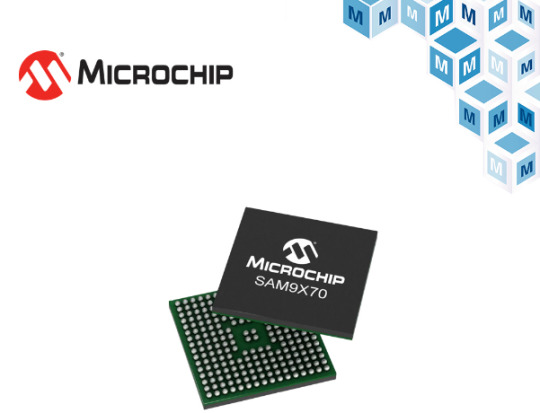
【Lansheng Technology News】On September 15, Microchip Technology released the SAM9X70 series MPU, which combines high performance, low power consumption, low system cost and high value. With the support of the powerful 800MHz Arm Thumb® processor, it provides a range of impressive connectivity options, rich user interface features and outstanding security features.
Microchip Technology SAM9X70 MPU is equipped with the ARM926EJ-S core, the CPU operating frequency is up to 800 MHz, and the system processing frequency is up to 266 MHz. On-chip memory includes 176-KB internal ROM, 64-KB internal SRAM, DDR3(L)/DDR2 controller and external bus interface (EBI). This MPU also supports various non-volatile memory (NVM) interfaces, including NAND flash, Quad SPI and eMMC flash. The SAM9X70 MPU achieves ultra-low power consumption through a real-time clock (RTC), 32-bit GP register, clock generator, power management controller, and software-programmable ultra-low power modes and optimization features.
In addition to its powerful processing capabilities and ultra-low power consumption features, what further enhances the performance of the SAM9X70 series is its rich on-chip peripheral interfaces. This series of MPUs feature 10/100/1000 Mbps Ethernet interfaces and support Time Sensitive Networking (TSN) connections, providing stable message delivery over standard Ethernet networks. The devices also offer MIPI-DSI, LVDS, RGB and 2D graphics interfaces, MIPI-CSI-2, Gigabit Ethernet with TSN and CAN-FD support for connectivity and user interface applications. Other connectivity options include an LCD controller, an image sensor controller, 13 FLEXCOMs, an ADC, a PWM controller, a Hi-Speed USB device/three Hi-Speed USB hosts, and more.
In addition to connecting peripherals, the SAM9X70 series also has powerful security features, such as secure boot using on-chip secure key storage (OTP), which can effectively prevent unauthorized users from stealing keys; high-performance encryption accelerators (SHA, AES and TDES) to protect confidential information and encrypt sensitive data. Additional security features include tamper protection and a Physical Unclonable Function (PUF) that generates keys on demand and clears them immediately after use.
Microchip Technology SAM9X70 MPU is available in a 240-ball BGA package. These MPUs are ideal for Internet of Things (IoT) applications, automotive, connected devices and user interfaces.
The SAM9X70 family is supported by Microchip MPLAB®-X development tools, Harmony, Linux® distributions and Ensemble Graphics Toolkit. When used with power management integrated circuits (PMICs) such as the MCP16501 and MCP16502, the SAM9X70's power-sequencing capabilities provide a fully tested power management solution.
Lansheng Technology Limited, which is a spot stock distributor of many well-known brands, we have price advantage of the first-hand spot channel, and have technical supports.
Our main brands: STMicroelectronics, Toshiba, Microchip, Vishay, Marvell, ON Semiconductor, AOS, DIODES, Murata, Samsung, Hyundai/Hynix, Xilinx, Micron, Infinone, Texas Instruments, ADI, Maxim Integrated, NXP, etc
To learn more about our products, services, and capabilities, please visit our website at http://www.lanshengic.com
0 notes
Text
SPI flash programmer software
My studies over the past few months have about understood; wire cable assembly, SPI flash programmer software and Circuit Protection Devices, Fuse Holders, Clips & Blocks, 83500000005, Littelfuse
0 notes
Text
Basic Understanding of AVR Microcontroller
AVR Microcontroller
If you are interested in learning how to program and control electronic devices, you might want to explore the world of AVR microcontrollers. These are small, low-cost and powerful chips that can be used for a variety of applications, such as robotics, home automation, gaming and more. In this blog post, I will give you a brief introduction to the basics of AVR microcontrollers and how to get started with them.
What is an AVR microcontroller?
A microcontroller is a device that contains a processor, memory and input/output peripherals on a single chip. It can be programmed to perform specific tasks by executing instructions stored in its memory. A microcontroller is different from a microprocessor, which is only the processor part and needs external components to function.
AVR is a family of microcontrollers developed by Atmel (now part of Microchip Technology). The name AVR comes from the initials of its creators: Alf-Egil Bogen and Vegard Wollan. AVR microcontrollers are based on the RISC (reduced instruction set computer) architecture, which means they have a simple and efficient instruction set that allows fast execution of code. AVR microcontrollers are also known for their low power consumption, high performance and ease of use.
Some of the features of AVR microcontrollers are:
- 8-bit or 32-bit processor cores - Flash memory for storing program code - SRAM for storing data - EEPROM for storing non-volatile data - GPIO (general purpose input/output) pins for interfacing with external devices - ADC (analog to digital converter) for reading analog signals - PWM (pulse width modulation) for generating analog signals - Timers and counters for measuring time and frequency - UART (universal asynchronous receiver/transmitter) for serial communication - SPI (serial peripheral interface) and I2C (inter-integrated circuit) for communication with other chips - Interrupts for responding to external events - Watchdog timer for resetting the device in case of errors
How to get started with AVR microcontrollers?
To start working with AVR microcontrollers, you will need some hardware and software tools. Here are some of the essential ones:
- An AVR microcontroller chip. You can choose from a wide range of models depending on your needs and budget. Some popular ones are ATmega328P (used in Arduino Uno), ATtiny85 (used in Digispark), ATmega2560 (used in Arduino Mega) and ATmega32U4 (used in Arduino Leonardo). - A programmer. This is a device that connects your computer to the microcontroller and transfers the program code to its memory. You can use a dedicated programmer, such as USBasp or AVRISP mkII, or an Arduino board as a programmer. - A breadboard. This is a board with holes that allow you to insert wires and components without soldering. You can use it to build circuits and connect your microcontroller to other devices. - A power supply. You can use batteries, USB cables or wall adapters to provide power to your microcontroller and circuit. - Some LEDs, resistors, capacitors, switches, sensors and other components. These are useful for creating various projects and experiments with your microcontroller. - An IDE (integrated development environment). This is a software that allows you to write, compile and upload your code to your microcontroller. You can use the official Arduino IDE, which supports many AVR models, or other alternatives, such as Atmel Studio or CodeVisionAVR. - A library or framework. This is a collection of code that simplifies the programming of your microcontroller by providing predefined functions and variables. You can use the Arduino core library, which is compatible with many AVR models, or other libraries, such as avr-libc or avr-gcc.
Once you have these tools ready, you can follow these steps to program your AVR microcontroller:
1. Connect your programmer to your computer and your microcontroller to your programmer. 2. Launch your IDE and create a new project or sketch. 3. Write your code using the syntax and functions of your chosen library or framework. 4. Compile your code and check for errors or warnings. 5. Upload your code to your microcontroller using your programmer. 6. Test your code by observing the behavior of your microcontroller and circuit.
Congratulations! You have just programmed your first AVR microcontroller!
What can you do with AVR microcontrollers?
The possibilities are endless! You can use AVR microcontrollers for various purposes, such as:
Making interactive gadgets and toys - Controlling motors, servos and relays - Reading sensors and displaying data - Communicating with other devices via Bluetooth, Wi-Fi or radio - Creating musical instruments and sound effects
If you are interested to understand more about the AVR microcontrollers, then you can go through the PiEmbSysTech AVR microcontrollers Tutorial Blog. If you have any questions or query, that you need to get answer or you have any idea to share it with the community, you can use Piest Forum.
0 notes
Text
.@googleai @google @googleuk @ai @california @texas @wired @wireduk #muffin_with_3_be rries_or_Chiuaua_or_someKindOfBowlingBallToBuy "ok google: ezp2019 and ch341a donot n eed software for linux flashrom: which -p device option for ezp 2019" https://www.flashrom.org › Flas hrom flashrom 31 Mar 2022 — flashrom is a u tility for identifying, reading, writing, verifying and erasing fl ash chips. It is designed to flash ... Missing: option | Must include: option https://winraid.level1techs .com › gui... Guide Using CH341A-based programmer to flash SPI EEPROM Hey all, I have been trying many many times but no success trying to flash a W25Q 128FV. I used different hardware (TL866 / EZP2019 and the black CH341a) and ... https: //www.amazon.ca › KeeYees-S... KeeYees SOP8 SOIC8 Test Clip and CH341A USB Programmer Flash ... This SOP8 clip is a great solution to program the chip without disassembly, no need for re-soldering, making the flash BI OS simpler and more efficient. We ... 4,3(436) · CA$28.99 Peopl e also search for Flashrom programmer Flashrom error Flashrom F T232H Bash flashrom command not found Coreboot flashrom AsProgrammer check settings Notices about Filtered Results In order to show you the most relevant results, we have omitted some entries very similar to the 3 already displayed. If you like, you can repeat the search with the omitted results included. Flashrom https: //www.flashrom.org › Flashrom flashrom 31 Mar 2022 — flashrom is a utility for identifying, reading, writin g, verifying and erasing flash chips. It is designed to flash ... Missing: option | Must include: option  winraid.level1techs.com https://winraid. level1techs.com › gu... Guide Using CH341A-based programmer to fla sh SPI EEPROM Hey all, I have been trying many many times but no success trying to fl ash a W25Q128FV. I used different hardware (TL866 / EZP2019 and the black CH341a) and ... (TL866 / EZP2019 and the black CH341a) and ...  Amazon.ca https://www.amazon.ca › KeeYees-... KeeYees SOP8 SOIC8 Test Clip and CH341A USB Programmer Flash for Most ... This SOP8 clip is a great solution to prog ram the chip without disassembly, no need for re-soldering, making the flash BIOS simpl er and more efficient. We ... 4,3(436) · CA$ 28.99 https://www.amazon.ca › KeeYees-... KeeYees SOP8 SOIC8 Clip de test et flash programmeur USB CH341A pour la ... It works w ith no trouble, once I managed to wire it to the EPROM chip in question. The Alternative was to pay a dealership almost $3,000 to install and ... 4,3(422) I am Christian KISS BabyAWACS – Raw Independent Sophistication #THINKTANK + #INTEL #HELLHOLE #BLOG http s://www.BabyAWACS.com/ [email protected] PHONE / FAX +493212 611 34 64 Helpful? Pay . Support. Donnate. paypal.me/ChristianKiss
.@googleai @google @googleuk @ai @california @texas @wired @wireduk #muffin_with_3_be rries_or_Chiuaua_or_someKindOfBowlingBallToBuy “ok google: ezp2019 and ch341a donot n eed software for linux flashrom: which -p device option for ezp 2019” https://www.flashrom.org › Flas hrom flashrom 31 Mar 2022 — flashrom is a u tility for identifying, reading, writing, verifying and erasing fl ash chips. It is designed to flash … Missing: option | Must include: option https://winraid.level1techs .com › gui… Guide Using CH341A-based programmer to flash SPI EEPROM Hey all, I have been trying many many times but no success trying to flash a W25Q 128FV. I used different hardware (TL866 / EZP2019 and the black CH341a) and … https: //www.amazon.ca › KeeYees-S… KeeYees SOP8 SOIC8 Test Clip and CH341A USB Programmer Flash … This SOP8 clip is a great solution to program the chip without disassembly, no need for re-soldering, making the flash BI OS simpler and more efficient. We … 4,3(436) · CA$28.99 Peopl e also search for Flashrom programmer Flashrom error Flashrom F T232H Bash flashrom command not found Coreboot flashrom AsProgrammer check settings Notices about Filtered Results In order to show you the most relevant results, we have omitted some entries very similar to the 3 already displayed. If you like, you can repeat the search with the omitted results included. Flashrom https: //www.flashrom.org › Flashrom flashrom 31 Mar 2022 — flashrom is a utility for identifying, reading, writin g, verifying and erasing flash chips. It is designed to flash … Missing: option | Must include: option  winraid.level1techs.com https://winraid. level1techs.com › gu… Guide Using CH341A-based programmer to fla sh SPI EEPROM Hey all, I have been trying many many times but no success trying to fl ash a W25Q128FV. I used different hardware (TL866 / EZP2019 and the black CH341a) and … (TL866 / EZP2019 and the black CH341a) and …  Amazon.ca https://www.amazon.ca › KeeYees-… KeeYees SOP8 SOIC8 Test Clip and CH341A USB Programmer Flash for Most … This SOP8 clip is a great solution to prog ram the chip without disassembly, no need for re-soldering, making the flash BIOS simpl er and more efficient. We … 4,3(436) · CA$ 28.99 https://www.amazon.ca › KeeYees-… KeeYees SOP8 SOIC8 Clip de test et flash programmeur USB CH341A pour la … It works w ith no trouble, once I managed to wire it to the EPROM chip in question. The Alternative was to pay a dealership almost $3,000 to install and … 4,3(422) I am Christian KISS BabyAWACS – Raw Independent Sophistication #THINKTANK + #INTEL #HELLHOLE #BLOG http s://www.BabyAWACS.com/ [email protected] PHONE / FAX +493212 611 34 64 Helpful? Pay . Support. Donnate. paypal.me/ChristianKiss
.@googleai @google @googleuk @ai @california @texas @wired @wireduk #muffin_with_3_berries_or_Chiuaua_or_someKindOfBowlingBallToBuy “ok google: ezp2019 and ch341a donot need software for linux flashrom: which -p device option for ezp2019” https://www.flashrom.org › Flashrom flashrom 31 Mar 2022 — flashrom is a utility for identifying, reading, writing, verifying and erasing flash chips. It is…
View On WordPress
0 notes
Text
SD, eMMC Host and Device Controller IP Cores Available for License
T2MIP, the global independent semiconductor IP Cores provider & Technology experts, is pleased to announce the immediate availability of its partner’s JEDEC standard SD/eMMC Host and Device Controllers with Matching PHY IP Cores which are silicon proven in major Fabs and Nodes and has been in Production in multiple chipsets with High storage capability making it a viable solution to integrate and implement in a varied range of applications.
SD/eMMC v5.1 Host & Device IP Cores are an embedded non-volatile memory system, comprised of both flash memory and a flash memory controller, which implements the Host and Device Controller IPs with high-speed processing power by complementing each core and makes the interface design with the Physical layer a lot less complex. This exempts Product developers from the hassle of integration, following to a diminished time-to-market.

Our SD/eMMC Host & Device Controllers and PHY IP Cores are specially designed for the eMMC v5.1 to augment its storage with SD v5.1 features to address the increasing storage needs of mobile, consumer, IoT and automotive applications. The eMMC 5.1 is compliant with JEDEC Standard JESD84-B51 and the Secure Digital (SD) part supports SD5.1 and later specifications (Class 1, Video Speed Performance) allowing the selection of either SD or SPI mode. To store and transfer data securely, the SD/eMMC IP Cores provide both data write protection and password protection. The multiple bus-width feature allows Host and Device design flexibility and higher data transfer bandwidth.
The SD/eMMC Host & Device Controllers with matching PHY IP Cores supports High-Speed Dual Data Rate transfer (52MHz), Single date rate transfer (200MHz) for eMMC and Default Speed mode (25 MHz, up to 12.5 MB/sec), High Speed mode (50 MHz, up to 25 MB/sec) for SD. The SD/eMMC IP Cores boasts low cost, low power and comparably low area making it feasible for portable and space-constrained products.
SD/eMMC Host & Device Controllers and PHY IP cores have been used in semiconductor industry’s Cellular Electronics, IoT Sensors, Navigational systems, Consumer electronics, handheld computers, and other industrial uses…
In addition to SD/eMMC IP Cores, T2M ‘s broad silicon Interface IP Core Portfolio includes USB, HDMI, Display Port, MIPI (CSI, DSI, UniPro, UFS, Soundwire, I3C), PCIe, DDR, 10/100/1000 Ethernet, V-by-One, programmable SerDes, OnFi and many more, available in major Fabs in process geometries as small as 7nm. They can also be ported to other foundries and leading-edge processes nodes on request.
Availability: These Semiconductor Interface IP Cores are available for immediate licensing either stand alone or with pre-integrated Controllers and PHYs. For more information on licensing options and pricing please drop a request / MailTo
About T2M: T2MIP is the global independent semiconductor technology experts, supplying complex semiconductor IP Cores, Software, KGD and disruptive technologies enabling accelerated development of your Wearables, IOT, Communications, Storage, Servers, Networking, TV, STB and Satellite SoCs. For more information, please visit: www.t-2-m.com
1 note
·
View note
Text
Standard SPI NOR Flash
I have interesting in these 'subjects; Macronix, MX25L12845GM2I-10GTR, NOR Flash Memory, Serial NOR Flash (SPI) Memory, Standard SPI NOR Flash and SPI programmer software.
0 notes
Text
Microchip Sound Cards & Media Devices Driver Download

60 Seconds Voice Recording Module, DIY Sound Recording Greeting Card Chip, Recordable Light Voice Sound Chip Module Replacement 3.9 out of 5 stars 22 $10.99 $ 10. The IBM Music Feature card is one of the original sound cards. This fairly expensive card includes an eight-voice stereo synthesizer and a complete MIDI interface. The heart of this card is the Yamaha YM-2164 sound chip, which can also be found in the Yamaha FB-01 MIDI Expander. Aug 08, 2019 The sound card in your computer is responsible for controlling and processing the input and output of all audio on your machine. If you’re having problems with audio on your computer, or have recently installed a new sound card, you can verify that the sound card is being detected by Windows. Method 1 Windows 8.
> Sound button
> sound book
prevnext
Introduction:Item:voice recordable musical chipMaterial:plastic & metalSize:30*40mm/customizedSwitch:Button/magnetic switch/Slide switchSound length:10-1800s/customize
Custom programmable Recording Sound chip for Greeting Card
Product description
Item
voice recordable musical Sound chip
Material
plastic & metal
Size
30*40mm/customized
Switch
Button/magnetic switch/Slide switch
Sound length
10-1800s/customize
Iife time
500 times more or less
Packing
EPE packaging and outside carton
Certification
CE,RoHS,FCC.
Power:
3*AG13/AG10
Application
recordable cards and sound toys etc
OEM or ODM
Welcome
MOQ
1000pcs
Picture
Two buttons voice Recording chip
Packaging & Delivery
Packing details
EPE and outside cartoon or customized
Shipping details
By regular air/ By sea/ By international express
Delivery detail
15-25 days
How to record by yourself
1.Pull out the insulation slices
2.Record your own message by pressing button.
3.Press another button play the message.
Ways to pre-record
We offer the musical chip can be designed to connected with a microphone / a usb cable or a TF card.
1. Microphone
A record button would be designed to record your own voice or sound source. Broadcast quality depends on entry of audio quality and environmental noise.
2. IC
Send us your sound source,we insert the sound source into IC.
3. USB
Uploaded the sound source to your computer(sound source can recorded by your cell-phone), then copy to your removable disk directly. The sound duration can be customized.
4. TF card
Download the music to TF card, and insert the card to module, then the module will play music which inside the TF card.
Why choose us:
1. We are the manufacturer of customized sound & luminous module, electronic gifts & toys and so on.
2. Our company develop and design customized products independently, which with high quality and reasonable price.
3. Professional team has more experience with more than 10 years development.
4. Skillful workers ensure quality and speed.
5. Customer satisfaction is our top priority.
6. Rapid response is our working standard.
Company introduction
Shenzhen Xinditai Electronic Co.,Ltd. Established in 2001, We are professional manufacturer of sound & luminous modules, and expert custom solutions provider of sound&luminous modules with high quality and reasonable price in Shenzhen of China Mainland. We have a series of products from musical chip, recording sound modules, voice recognition module,USB audio module, download sound chip, recordable greeting card, squeeze box music, led flashing modules for toys, gifts and cards to Bluetooth player, etc.
FAQ
Q: Are you a factory or a trading company? A: We have own company and factory that we can provide perfect OEM and after-sale service. Q: Sample time and price? A: Will according to your design about 5-7 days. Q: What is your MOQ and delivery time? A: MOQ is 1000 pcs. 10-15 days for minimum order quantity. Q: How can I pay my order? A: We accept T/T, Western Union paying methods. For those orders less than 1000 USD, we accept PayPal to pay. Q: Do you have certificate? A: All of our product has CE, RoHS and FCC certificate.
Contact information
Shenzhen XindiTai Electronics Co., Ltd. Add: Floor 3-4, No. 12, Lane 1, Nanlian Baolong Community, Longgang Street, Longgang District,Shenzhen,China Telephone: 0086-755- 8989-1700
0086-755- 8989-1702
Mobile:+0086-157 28259858 (Whatsapp)
A Microchip PIC based USB sound card
INTRODUCTION
The idea for creating a USB sound card based on a PIC came from discussions of other people creating one on the Microchip USB forum. The hardware of the card is based on all Microchip products. The software uses a modified version of the Microchip USB framework which is interrupt driven instead of the traditional polling. The device is a USB composite device. The first device is an implementation of the USB Audio 1.0 interface and the other device is a custom interface based on a HID interface. The purpose of the custom interface is for programming the device serial number, upgrading the firmware, and in the future any other configuration that isn’t supported directly by USB Audio 1.0. In a previous version, WinHTTP was oringally used. After testing the card for awhile, I decided it's better to not require drivers for the card especially since the HID/WinUSB interface is rarely used.
The sound card runs at a sample rate of 48KHz, 32KHz or 24KHz selectable by the OS with 12 bits per sample. The quality approaches commercial grade as the sample rate is higher then CDs. 44.1KHz was not implemented due to the difficultly and additional processing overhead. The sample rates that were implemented are all a multiple of the 1ms USB frame meaning each frame sends the same amount of data. 44.1KHz requires the card to handle different amounts of data each frame requiring more advanced buffering and synchronization techniques and more processing power. Microsoft Windows automatically resamples the 44.1KHz audio found on CDs to 48KHz.
USB Audio Streamer V1.2
HARDWARE
Click for enlarge Schematic for USB Audio Streamer V1.2
The hardware for the sound card is based on the Microchip PIC18F2550 USB processor. The processor is clocked at 48MHz which is the maximum rate for this processor and is also a multiple of the audio sample rate. The microcontroller is connected via the SPI port to duel Microchip MCP4822 12bit D/A converters. Volume control is implemented by the Microchip MCP41010 variable res-- ders are controlled via SPI by the microcontroller via a dedicated bit-banged SPI port. The purpose of using a separate port is so that volume control can run inside the processor at a different priority level then sample output. The Microchip MCP6022 op-amp is used as an output driver.
The MCP6022 op-amp has an output drive capacity large enough to power a pair of cheap headphones without much distortion. The resistance of my headphones is approximately 25ohms. The op-amps are not powerful enough to drive speakers which are usually 8 or 4 ohms. The MCP41010 and MCP6022 can output near rail to rail voltage although some nonlinear effects can be heard if the volume is too loud or the signal is near the minimum or maximum. Since USB has a single rail 5V power supply, the sound card only uses a positive rail instead of a traditional duel rail system which is how standard 16bit PCM is encoded. As a result, the signal needs to be biased in software to 2.5V.
One terminal of the MCP41010 is connected to the signal for that channel and the other terminal is connected to the midpoint or bias voltage. Previous versions of this sound card connected the second terminal to GND. The advantage of connecting the terminal to the bias is that as the volume is changed, the signal grows or shrinks around the midpoint rather then shifting toward GND. The signal is kept as far away from the rails as possible.
SOFTWARE
The software for USB Audio Streamer is composed of several components. These are the audio card firmware, a C++ library that wraps HID and WinUSB, and a command line utility for flashing. I am giving out the source code as a learning tool for other people. I don’t care what you do with it but I am not responsible for any damage that might happen from using it. NOTE: Improper use of hardware or software may cause serious injury or death.:)
I use Visual Studio 2005 Professional but I have heard that the project will build with Visual Studio Express. To build the project it is necessary to download the latest version of the WDK to get the headers and library files for HID and WinUSB. The default directories in Visual studio need to be modified to point to the directories of these resources in the WDK. If you use Visual Studio Express it's necessary to recreate all the project files and change the default calling convention to _stdcall.
DirectoryFunctionincGeneral Include DirectorybootBoot Loader(Build first)audiostreamSound card firmwareusbdevprogramerProgrammer command line utility(Build last)
Source Code Modules
A trick is used when building the sound card firmware since it is two separate projects that need to be merged together. Build the boot directory first, which is the code responsible for upgrading the firmware. Then build the sound card firmware itself. Before flashing, goto Configure/Settings/Program Loading and clear the option to clear program memory upon loading a new program. After the sound card firmware is build, goto file/import and import the hex file for the boot loader. The two projects will be merged together without any cutting and pasting. At this point, it is OK to flash the PIC. Note the bootloader is only necessary for flashing firmwares without a ICD/Pickit. When debugging actual card functionality, it's ok to leave out the bootloader. This Requires no modifications to the sounce or linker scripts. Simply don't merge the boot loader into the image
SOUND CARD FIRMWARE
The sound card firmware is based on a modified version of the Microchip USB framework. The framework has been collapsed into a single source file with callbacks between the framework and the main code. The framework( in my case it’s more of a library ) has been modified to use interrupts instead of the traditional polling method. Instead of calling USBDriverService in a loop, this function is called whenever the USB interrupt fires. The library is response for handling control requests on endpoint 0. The framework handles standard USB requests and the body code is responsible for handling class specific USB requests nonstandard requests. The body code is responsible for handling I/O on all other endpoints.
USB Audio Streamer is a composite device of a USB Audio 1.0 device and a custom HID interface. With USB Audio 1.0 all of the sample data is transferred through a separate endpoint then control requests. Control requests such as controlling volume is through endpoint 0(the control endpoint.) HID uses it’s own endpoint. Since each function of the card has a separate endpoint, each of the functions can be implemented at a different priority level without preemption problems. The PIC18F2550 has two interrupt priorities plus the main handler. This gives a total of three priorities. Since playing sound data is the most critical function it was given the highest priority. Next comes control endpoint requests which include the standard requests plus Audio 1.0 requests. Since these functions have relatively low timeouts, these were assigned low priority. HID functions are in the main body code because actions such as querying the firmware version, settings the serial number, or flashing the firmware are not time critical at all.
EndpointPriorityFunctionEP 2Interrupt(High)Streams the audio data to the D/A converterEP 0Interrupt(Low)Control Endpoint function and Audio 1.0 requestsEP 1Main(Background)Non standard functions
Endpoints, priorities, and functions of firmware

CORE AUDIO
The low priority interrupt handler performs two functions. The first is to check the ISO endpoint through the SIE for data. If data is available the buffer is passed to the high priority interupt code and next buffer that makes up a cicular queue is returned to the SIE. The buffers are in the USB ram of the PIC so that the data is not copied between buffers. In Audio 1.0, the host always sends exactly the number of samples to fit in a frame which is 196, 128 or 96 bytes depending on the sample rate used.
The second function of the low priority interrupt handler is SOF(start of frame) processing. Upon receiving the SOF, the PIC changes the current play buffer to the next available buffer and starts timer 2 which is the sample clock. Timer 2 is always reset on the SOF to keep the sample clock synchronized when clock drift is present. If the SOF occurs before the current buffer is played, playback is changed to the next buffer. If the SOF occurs after the buffer is finished, the last sample is stretch. Since the clock drift is normally small, most of the time samples are not dropped. The time of the last sample is slightly different. This is not noticeable in the audio and is only barely noticeable when playing SIN waves.
The high priority interrupt is driven off timer 2 and has the function of formating the data in the format required by the converter and loading the D/A converter through the SPI port of the PIC. The samples are converted from 16 bits signed PCM to 12 bit unsigned and the endianess is swapped. After the buffer is finished, timer 2 is stopped so that if the clock of the card is ahead of the host, the last sample is stretched.
AUDIO 1.0 REQUESTS
All Audio 1.0 requests are handled via an extension of the USB framework. The low priority interrupt calls USBDriverService which services the control request. If the request is a standard USB request, the request is handled by the framework. If it isn't, the framework calls back into the main code which examines the request. If the request is recognized, the main code claims the request. If the request is a read request, the main body sets the address of a variable to sent to the host. If it's a write request, a variable is written to but the firmware sets a completion routine to be called at the end of the request.
The card only handles two types of requests which are volume control and sample rate selection. The current value of both of these is stored in a global variable. If the volume is adjusted, new values are loaded into the variable resistors. If the sampling rate is adjusted, a new period is loaded into PR2 for timer 2.
HID REQUESTS AND HOST SOFTWARE
The main body code polls endpoint 1 for custom requests in a loop. If the request is anything other then setting the serial or flashing the firmware, the request is handled in the main body code. Otherwise, the processor is put into a special programming mode. Upon entering this mode, all interrupts are disabled and the USB library is used in the traditional polling mode as program memory blocks are moved from the host. Flashing the microcontroller is reusable code that is used for multiple projects.
The host side consists of a C++ library that wraps HID and a command line C utility for configuring the card. These utilities are used for multiple projects and will be discussed in a separate topic.
TESTING 123...
The USB Audio Streamer uses instrumentation grade analog components so frequency response is not a major concern. The main concern is noise and signal accuracy due to nonlinear properties of the components, jitter, and that the sample clock can drift from the USB SOF clock.
To measure the accuracy, I used Audicity to play 20 second sin tones of various frequencies and recorded the output on a Dell laptop with a built-in 24bit 96KHz Sigmatel sound card. The assumption is that the 24bit sound card is much better then the USB hardware. The output was recorded with Audicity and the spectrum of the signal plotted. The idea is that perfect hardware would have a single peak at the tone’s frequency and nothing elsewhere. The experiment was performed with both the USB Audio Streamer and a commercial 16 bit USB sound card the Turtle Beach Audio Advantage. In all cases, a 48KHz sample rate was used. In the follow graphs, the Audio Streamer is on the left and the Turtle Beach is on the right.
Click for enlarge Click for enlarge 1KHz SIN
Click for enlarge Click for enlarge 4KHz SIN
Click for enlarge Click for enlarge 20KHz SIN
Cards With Sound
As can be seen, the accuracy of both devices decreases as the tone’s frequency is increased. Up to about 12KHz, both devices have approximately the same noise floor. At 12KHz though, the Audio Streamer’s performance begins to rapidly diminish. Both devices are isosynchronous adaptive, but apparently the Turtle Beach has better drift control algorithms. At 20KHz, even the Turtle Beach has noise of -40dB which is not that good. It seems that designing a high quality USB audio device is very difficult even for commercial developers.
Microchip Sound Cards For Kids
Tone FrequencyAudio StreamerTurtle Beach1KHz-50dB-55dB2KHz-50dB-55dB4KHz-45dB-50dB8KHz-40dB-40dB12KHz-35dB-45dB16KHz-30dB-40dB20Hz-25dB-40dB
0 notes
Text
Microcontroller SAMD21 (XIAO) von Seeedstudio

In diesem Beitrag möchte ich dir den kleinen Microcontroller SAMD21 von der Firma Seeedstudio vorstellen.

Seeedstudio SAMD21 (XIAO)
Bezug des SAMD21
Den SAMD21 habe ich über aliexpress.com für knapp 5€ inkl. Versandkosten erstanden. Du findest diesen aber auch auf ebay.de für einen Preis von 6€ zzgl. Versandkosten. Lieferumfang Zum Lieferumfang gehört neben dem Microcontroller zwei kleine 7 polige Stiftleisten noch 3 Aufkleber welche die Pinbelegung des SAMD21 aufzeigt.

Lieferumfang des SAMD21
technische Daten des SAMD21
CPU ARM Cortex-M0+-CPU(SAMD21G18) Geschwindigkeit bis zu 48 MHz Speicher Flash 256KB SRAM 32KB Schnittstellen I²C, UART, SPI digitale I/O Pins 11 analoge I/O Pins 11 Stromversorgung / USB Schnittstelle USB Typ C Betriebsspannung 3,3V / 5V DC Abmaße (LxBxH) 20mm x 17mm x 3,5mm
Aufbau
Auf der Vorderseite des Microcontrollers sind neben den beiden SMD LEDs auch die Lötpunkte für den RESET Taster angebracht.

aktive LEDs auf der Vorderseite des SAMD21 Auf der Rückseite findest du die Beschriftung der Pins sowie weitere Lötpunkte für die Stromversorgung und die SPI Kontakte.

Rückseite des XIAO SAMD21 mit Pinbeschriftung Pinout des SAMD21 Zum vergrößern des Bildes, bitte auf das Bild klicken!

Pinout des Microcontroler SAMD21 (XIAO) von Seeedstudio Auf der Rückseite des SAMD21 sind 6 Lötpunkte von welchen 2 mit jeweils "VIN" für die Spannungsversorgung (ohne USB betrieb) und "GND" beschriftet sind, die anderen 4 Lötpunkte sind nicht beschriftet.

Pinout des SAMD21 auf der Rückseite LEDs auf dem SAMD21 Auf dem SAMD21 sind vier SMD LEDs verbaut welche mit den Buchstaben P, R, L & T beschriftet sind. Was die Buchstaben bedeuten kannst du aus der nachfolgenden Grafik entnehmen.

SMD LEDs am SAMD21 XIAO Die interne LED kannst du über den Pin D13 ansteuern (siehe Beispiel "interne LED blinken lassen").
Einrichten auf dem Computer
Der Microcontroller verfügt über eine USB Typ C Schnittstelle und wird mit einem entsprechenden Kabel (nicht im Lieferumfang enthalten) mit dem Computer verbunden. Unter Microsoft Windows 10 wird dieser als "Seeed femto M0" erkannt und eingerichtet.

MS Windows 10 - Gerät "SAMD21" eingerichtet Im Geräte-Manager wird dieser bei mir als "Serielles USB-Gerät" angezeigt.

Windows 10 - Geräte-Manager mit eingerichtetem SAMD21 am COM5 Einrichten von CircuitPython Auf diesem kleinen Zwerg kannst du mit der Skriptsprache Python bzw. MicroPython programmieren. Dafür musst du jedoch zunächst die Firmware einrichten. Das ist recht einfach und in wenigen Schritten erledigt. Gehe zunächst auf die Seite https://circuitpython.org/board/seeeduino_xiao/ und lade dir die ca. 360 KB große Datei "adafruit-circuitpython-seeeduino_xiao-de_DE-6.0.1.uf2" herunter. Wenn du diese Datei heruntergeladen hast, dann musst du deinen SAMD21 mit dem Computer verbinden (soweit noch nicht geschehen) und dir ein kurzes Breadboardkabel mit Steckern besorgen und deinen Windows Explorer öffnen. Auf der Vorderseite sind zwei Lötpunkte mit der Beschriftung "RST" versehen diese musst du nun zwei mal kurz Verbinden / Kurzschließen. Es sollte nun ein zusätzliches Laufwerk "Arduino" angezeigt werden. In dieses Laufwerk kopieren wir nun die heruntergeladene *.uf2 Datei wobei danach das Laufwerk wieder "verschwindet" und kurz darauf der Microcontroller als "Seeedstudio XIAO" erkannt wird und das Laufwerk "CIRCUITPY" angezeigt wird.

Eigenschaften des Laufwerks "CIRCUITPY" unter Windows 10 In dieses Laufwerk können wir nun unsere Python Datei kopieren welche sofort ausgeführt wird. Download und Installation vom Editor Mu Für die Programmierung auf dem SAMD21 kannst du den kostenfreien Editor "Mu" verwenden. Diesen Editor kannst du unter https://codewith.mu/en/download für Windows bzw. Mac herunterladen. Ich verwende einen MS Windows 10 PC mit 64bit und lade mir somit die Version "Windows 64-bit" herunter. Solltest du ein 32bit System verwenden oder nicht genau wissen ob du ein 64 oder 32bit System hast, so empfehle ich dir die 32bit Version welche auf beiden Systemen reibungslos laufen sollte. Nachdem die ca. 65 MB große Datei heruntergeladen wurde muss diese mit einem Doppelklick geöffnet werden. Es startet dann nach einer kurzen Abfrage der Installer. erster Start des Editors Mu Wenn die Installation abgeschlossen ist, dann kann der Editor gestartet werden. Und zunächst wird man aufgefordert einen Modus wählen.

Editor Mu - wählen des Modus In unserem Fall wählen wir aus der Liste den Eintrag "CircuitPython" und bestätigen die Auswahl mit der Schaltfläche "OK". Wenn dein Microcontroller bereits mit dem Computer verbunden ist dann kannst du quasi sofort loslegen, ansonsten erscheint ein Dialog welcher darauf hinweist das kein Gerät verbunden ist.

Editor Mu - kein Gerät gefunden "Hello World!" mit dem Editor Mu auf dem SAMD21 Wollen wir nun unser erstes kleines Stück Code mit dem Editor Mu schreiben und auf den SAMD21 ausführen. Zunächst wollen wir den einfachen kleinen Text "Hello World!" auf der seriellen Schnittstelle ausgeben. Dazu schreiben wir print("Hello World!") und speichern die Datei als "code.py" auf dem Laufwerk "CIRCUITPY" ab. Der Editor Mu liefert zwar die Schaltfläche "Serial" aber leider erscheint dort immer nur eine Fehlermeldung, somit müssen wir uns anderweitig behelfen. Ich nutze hier die kostenfreie Software Putty mit welcher man sich ebenso mit dem Microcontroller verbinden kann.

Putty - Konfiguration für den SAMD21 Wichtig ist das die Baudrate / Speed auf 115200 eingestellt wird und das der COM-Port passt. Ggf. kannst du unter Windows im Geräte-Manager prüfen an welchem COM-Port dein Gerät erkannt wurde. Wenn das korrekt eingestellt ist kann die Verbindung mit der Schaltfläche "OK" aufgebaut werden. Es erscheint dann unsere Ausgabe auf dem Terminalfenster von Putty. Und jedesmal wenn wir am Code etwas ändern und im Editor Mu die Datei speichern wird der Code ausgeführt und das Fenster aktualisiert sich automatisch.
alternative über die Arduino IDE
Wenn dir Putty etwas zu umständlich ist, kannst du auch den seriellen Monitor aus der Arduino IDE nutzen. Zunächst musst du unter dem Menüpunkt "Werkzeuge" den Port des SAMD21 auswählen und startest den seriellen Monitor über die Lupe oben rechts, oder der Tastenkombination "Strg+Umschalt+M".

Editor "MU" mit Ausgabe der Daten im seriellen Monitor der Arduino IDE Der Code erzeugt nun alle 0,5 Sekunden eine Ausgabe auf der seriellen Schnittstelle welche von dem seriellen Monitor der Arduino IDE auf dem Bildschirm ausgegeben wird.
Beispiele mit dem SAMD21
Nachdem wir nun den SAMD21 eingerichtet und das erste kleine "Hallo Welt!" Programm auf diesem ausgeführt haben möchte ich dir nun ein paar kleine Beispiele zeigen welche du mit diesem Programmieren kannst. Ich habe die Pinleisten auf der Rückseite angelötet dieses ist entgegen der bekannten Richtung, das liegt vielmehr daran das der kleine Aufkleber garantiert nicht langlebig ist und somit die Pinbeschriftung auf der Rückseite sichtbar bleibt. Ich habe dir bereits in einigen Beispielen gezeigt wie du mit MicroPython Sensoren & Aktoren auf einem Microcontroller ansteuern bzw. auslesen kannst. Mit CiruitPython funktioniert dieses sehr sehr ähnlich und damit unterscheidet sich die Programmierung nur sehr marginal in zbsp. den verwendeten Bibliotheken. interne LED blinken lassen Im nachfolgenden Beispiel möchte ich nun zeigen wie du die interne LED am digitalen Pin D13 im Intervall von 0,5 Sekunden blinken lassen kannst. import time import board from digitalio import DigitalInOut, Direction # definieren des Pins led = DigitalInOut(board.D13) # definieren das der Pin als AUSGANG dient led.direction = Direction.OUTPUT while True: # aktivieren der LED led.value = True # eine Pause von 0,5 Sekunden time.sleep(0.5) # deaktivieren der LED led.value = False # eine Pause von 0,5 Sekunden time.sleep(0.5) Video LED Wechselblinken Ein großer Vorteil des kleinen SAMD21 ist das dieser auf ein Breadboard gesteckt werden kann (wie auch der Wemos D1 Mini / Pro, Arduino Micro / Nano). Aufbau der Schaltung Für den Aufbau der Schaltung benötigst du: - 2x LED, 5mm, - 2x Widerstand, 220 Ohm, - 5x Breadboardkabel, 10cm, männlich-männlich, - 1x Breadboard 170 Pin, - und natürlich einen Microcontroller SAMD21 :)

Schaltung - Wechselblinken am Microcontroller SAMD21 Quellcode import time import board from digitalio import DigitalInOut, Direction # definieren des Pins led1 = DigitalInOut(board.D5) led2 = DigitalInOut(board.D6) # definieren das der Pin als AUSGANG dient led1.direction = Direction.OUTPUT led2.direction = Direction.OUTPUT while True: # aktivieren der LED1 & deaktivieren der LED2 led1.value = True led2.value = False # eine Pause von 0,5 Sekunden time.sleep(0.5) # aktivieren der LED2 & deaktivieren der LED1 led1.value = False led2.value = True # eine Pause von 0,5 Sekunden time.sleep(0.5) Video auslesen des Temperatursensors TMP36 Als nächstes möchte ich dir zeigen, wie du die Werte eines analogen Temperatursensors TMP36 auslesen und auf der seriellen Schnittstelle ausgeben kannst. der analoge Temperatursensor TMP36 Der analoge Temperatursensor TMP36 verfügt über drei Pins an welche der Minuspol, der Pluspol (3,3V) sowie die Datenleitung angeschlossen wird. Bezug Den analogen Sensor kannst du bei ebay.de für bereits 1,5€ zzgl. Versandkosten erstehen. technische Daten des TMP36 - Betriebsspannung: 2,7V bis 5,5V - Stromaufnahme: maximal 0,5 µA - Toleranz: ±2°C - Messbereich: -40°C bis 125°C Pinout des analogen Temperatursensors TMP36

Pinout des analogen Temperatursensors TMP36 Aufbau der Schaltung Für den Aufbau der Schaltung benötigst du: - 1x analoger Temperatursensor TMP36, - 1x Breadboard, 170 Pin, - 3x Breadboardkabel, 10cm, männlich-männlich, - und natürlich einen Microcontroller SAMD21 :)

Aufbau der Schaltung - Sensor TMP36 am SAMD21

Aufbau der Schaltung - SAMD21 mit Sensor TMP36 Quellcode Den Quellcode habe ich von der Seite "TMP36 with CircuitPython" von Adafruit Learning System und habe diesen "nur" um Erläuterungen zum Quellcode sowie einigen kleineren Formatierungen der Ausgaben ergänzt. import board import analogio import time # Sensor TMP36 am analogen Pin A0 angeschlossen TMP36_PIN = board.A0 tmp36 = analogio.AnalogIn(TMP36_PIN) # Funktion zum berechnen der Temperatur # Zu dieser Berechnung wird die Referenzspannung am # Microcontroller verwendet, da der Sensor Stromabhängig # die Temperatur misst benötigt man die Referenzspannung def tmp36_temperature_C(analogin): millivolts = analogin.value * (analogin.reference_voltage * 1000 / 65535) return (millivolts - 500) / 10 # Endlosschleife counter = 0; while True: counter = counter + 1 # lesen der Temperatur in Grad Celsius temp_C = tmp36_temperature_C(tmp36) # Umwandeln der Temperatur in Grad Fahrenheit temp_F = (temp_C * 9/5) + 32 # Ausgeben der Temperatur print("#", str(counter), "t" , "%03.2f" % temp_C , "°C", "|", "%03.2f" % temp_F, "°F") # eine Pause von 1 Sekunde time.sleep(1.0) Video serieller Plotter der Arduino IDE Die Arduino IDE bietet neben dem seriellen Monitor zusätzlich auch einen seriellen Plotter welcher Zahlenwerte in einem Liniendiagramm anzeigen kann. Dabei muss man als erstes die Legende ausgeben und danach die Werte. Quellcode Damit wir die Daten in dem Liniendiagramm anzeigen lassen können, müssen wir den Quellcode etwas modifizieren. import board import analogio import time # Sensor TMP36 am analogen Pin A0 angeschlossen TMP36_PIN = board.A0 tmp36 = analogio.AnalogIn(TMP36_PIN) # Funktion zum berechnen der Temperatur # Zu dieser Berechnung wird die Referenzspannung am # Microcontroller verwendet, da der Sensor Stromabhängig # die Temperatur misst benötigt man die Referenzspannung def tmp36_temperature_C(analogin): millivolts = analogin.value * (analogin.reference_voltage * 1000 / 65535) return (millivolts - 500) / 10 # Endlosschleife while True: columns = "Celsius Fahrenheit" temp_C = tmp36_temperature_C(tmp36) temp_F = (temp_C * 9/5) + 32 print(columns) print("%03.2f" % temp_C ," ", "%03.2f" % temp_F) time.sleep(1.0) Ausgabe Read the full article
0 notes
Text
Microcontroller ATTINY44A
In almost every system existing today, an automatically controlled mechanism is preferred. From office to home they are used in every gadget to make our life less hectic, fast, and energy-efficient. Microprocessors and microcontrollers serve this purpose. ATTINY44A is a microcontroller with RAM, ROM, Input, and Output ports electronics supplies. Depending on the task, it is convenient to select the type of controller that fits well for the desired purpose. Generally, two parameters are kept in mind while selecting the controller's first power consumption and the other processing speed. Both are at the expense of one and another. ATTINY44A performs smartly between these parameters by executing powerful instructions in one clock because of its ability to optimize itself at the most efficient point. Furthermore, it has a variety of options and control capabilities. If one has extraordinary programming skills the ATTINY44A outperforms CISCs.

ATTINY44A is low power 8-bit, 14-pin PDIP/SOIC packaged AVR microcontroller, accredited to Microchip Technology Inc. famously known for microcontrollers and integrated circuits. With the invention of these modules, electronic tasks can be easily and readily achieved. Operating at a voltage range of 1.8V-5.5V. If the ATTINY44A is operating at 2.7 volts its speed grade ranges from 0 to 10MHz but if it is operating at less than the aforementioned volts its grading speed reduces from 0 to 4MHz.
Further details are thoroughly mentioned in the respective datasheet. It has Reduced Instruction Set Computer (RISC) architecture which gives a significant advantage of processing speed since Complex Instruction Set Computer (CISC) architecture is comparatively slow per instruction. Moreover, it upholds the advantage of using fewer transistors because it executes simple instructions and is thus relatively smaller in size. RISC-based architectures are easier to design and are available in a low purchasing range as compared to CISC-based microcontrollers. ATTINY44A has RISC architecture therefore it can be used for implementing multiple tasks. It executes powerful instructions of 120 in a clock cycle with full static operation. Furthermore, it has 32x8 general-purpose registers and a programmable watchdog timer.
Some other features are segments of non-volatile memory and high endurance. Its non-volatile memory segments include in-built flash memory of 4KB storage with 10,000 write and erase repetitions, in-built EEPROM of 256 bytes storage with 100,000 cycles, and in-built 256 bytes SRAM. It retains data according to the given temperature conditions. For example, it can keep data safe for 20 years at 85 degrees ⁰C and 100 years at 25 ⁰C. It has another great feature of locking self-programming characteristics concerned with EEPROM and flash memory to keep previous data secured. Its peripheral features incorporate 8-bit and 16-bit timer & counter, universal serial interface (USI), two PWM channels, ADC along with on-logic chip analog comparator and oscillator while its special features comprise of a debug system, SPI port, stand-by, and power-down modes, ADC noise reduction, an on- logic chip temperature sensor, reset circuit and brownout detection circuit along with software disable the function.
ATTINY44A is mainly used in automation industries for the production of abundant materials and goods in less time. It can be incorporated into various other fields such as robotics, aeronautics, and embedded systems. Its widely found application is in power management for careful monitoring and continuation of the system. It performs competently in silicon-organic hybrid voltage equalizer by protecting and balancing charging factors of super-capacitor for sale.
0 notes
Text
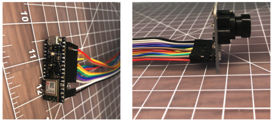
Optimizing a low-cost camera for machine vision
In this deep dive article, performance optimization specialist Larry Bank (a.k.a The Performance Whisperer) takes a look at the work he did for the Arduino team on the latest version of the Arduino_OV767x library.

Arduino recently announced an update to the Arduino_OV767x camera library that makes it possible to run machine vision using TensorFlow Lite Micro on your Arduino Nano 33 BLE board.
If you just want to try this and run machine learning on Arduino, you can skip to the project tutorial.
The rest of this article is going to look at some of the lower level optimization work that made this all possible. There are higher performance industrial-targeted options like the Arduino Portenta available for machine vision, but the Arduino Nano 33 BLE has sufficient performance with TensorFlow Lite Micro support ready in the Arduino IDE. Combined with an OV767x module makes a low-cost machine vision solution for lower frame-rate applications like the person detection example in TensorFlow Lite Micro.
Need for speed
Recent optimizations done by Google and Arm to the CMSIS-NN library also improved the TensorFlow Lite Micro inference speed by over 16x, and as a consequence bringing down inference time from 19 seconds to just 1.2 seconds on the Arduino Nano 33 BLE boards. By selecting the person_detection example in the Arduino_TensorFlowLite library, you are automatically including CMSIS-NN underneath and benefitting from these optimizations. The only difference you should see is that it runs a lot faster!
The CMSIS-NN library provides optimized neural network kernel implementations for all Arm’s Cortex-M processors, ranging from Cortex-M0 to Cortex-M55. The library utilizes the processor’s capabilities, such as DSP and M-Profile Vector (MVE) extensions, to enable the best possible performance.
The Arduino Nano 33 BLE board is powered by Arm Cortex-M4, which supports DSP extensions. That will enable the optimized kernels to perform multiple operations in one cycle using SIMD (Single Instruction Multiple Data) instructions. Another optimization technique used by the CMSIS-NN library is loop unrolling. These techniques combined will give us the following example where the SIMD instruction, SMLAD (Signed Multiply with Addition), is used together with loop unrolling to perform a matrix multiplication y=a*b, where
a=[1,2]
and
b=[3,5 4,6]
a, b are 8-bit values and y is a 32-bit value. With regular C, the code would look something like this:
for(i=0; i<2; ++i) for(j=0; j<2; ++j) y[i] += a[j] * b[j][i]
However, using loop unrolling and SIMD instructions, the loop will end up looking like this:
a_operand = a[0] | a[1] << 16 // put a[0], a[1] into one variable for(i=0; i<2; ++i) b_operand = b[0][i] | b[1][i] << 16 // vice versa for b y[i] = __SMLAD(a_operand, b_operand, y[i])
This code will save cycles due to
fewer for-loop checks
__SMLAD performs two multiply and accumulate in one cycle
This is a simplified example of how two of the CMSIS-NN optimization techniques are used.
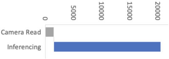
Figure 1: Performance with initial versions of libraries
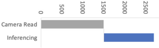
Figure 2: Performance with CMSIS-NN optimizations
This improvement means the image acquisition and preprocessing stages now have a proportionally bigger impact on machine vision performance. So in Arduino our objective was to improve the overall performance of machine vision inferencing on Arduino Nano BLE sense by optimizing the Arduino_OV767X library while maintaining the same library API, usability and stability.

Figure 3: Performance with CMSIS-NN and camera library optimizations
For this, we enlisted the help of Larry Bank who specializes in embedded software optimization. Larry’s work got the camera image read down from 1500ms to just 393ms for a QCIF (176×144 pixel) image. This was a great improvement!
Let’s have a look at how Larry approached the camera library optimization and how some of these techniques can apply to your Arduino code in general.
Performance optimizing Arduino code
It’s rarely practical or necessary to optimize every line of code you write. In fact there are very good reasons to prioritize readable, maintainable code. Being readable and optimized don’t necessarily have to be mutually exclusive. However, embedded systems have constrained resources, and when applications demand more performance, some trade-offs might have to be made. Sometimes it is necessary to restructure algorithms, pay attention to compiler behavior, or even analyze timing of machine code instructions in order to squeeze the most out of a microcontroller. In some cases this can make the code less readable — but the beauty of an Arduino library is that this can be abstracted (hidden) from user sketch code beneath the cleaner library function APIs.
What does “Camera.readFrame” do?
We’ve connected a camera to the Arduino. The Arduino_OV767X library sets up the camera and lets us transfer the raw image data from the camera into the Arduino Nano BLE memory. The smallest resolution setting, QCIF, is 176 x 144 pixels. Each pixel is encoded in 2 bytes. We therefore need to transfer at least 50688 bytes (176 x 144 x 2 ) every time we capture an image with Camera.readFrame. Because the function is performing a byte read operation over 50 thousand times per frame, the way it’s implemented has a big impact on performance. So let’s have a look at how we can most efficiently connect the camera to the Arduino and read a byte of data from it.
Philosophy
I tend to see the world of code through the “lens” of optimization. I’m not advocating for everyone to share my obsession with optimization. However, when it does become necessary, it’s helpful to understand details of the target hardware and CPU. What I often encounter with my clients is that their code implements their algorithm neatly and is very readable, but it’s not necessarily ‘performance friendly’ to the target machine. I assume this is because most people see code from a top-down approach: they think in terms of the abstract math and how to process the data. My history in working with very humble machines and later turning that into a career has flipped that narrative on its head. I see software from the bottom up: I think about how the memory, I/O and CPU registers interact to move and process the data used by the algorithm. It’s often possible to make dramatic improvements to the code execution speed without losing any of its readability. When your readable/maintainable solution still isn’t fast enough, the next phase is what I call ‘uglification.’ This involves writing code that takes advantage of specific features of the CPU and is nearly always more difficult to follow (at least at first glance!).
Optimization methodology
Optimization is an iterative process. I usually work in this order:
Test assumptions in the algorithm (sometimes requires tracing the data)
Make innocuous changes in the logic to better suit the CPU (e.g. change modulus to logical AND)
Flatten the hierarchy or simplify overly nested classes/structures
Test any slow/fast paths (aka statistics of the data — e.g. is 99% of the incoming data 0?)
Go back to the author(s) and challenge their decisions on data precision / storage
Make the code more suitable for the target architecture (e.g. 32 vs 64-bit CPU registers)
If necessary (and permitted by the client) use intrinsics or other CPU-specific features
Go back and test every assumption again
If you would like to investigate this topic further, I’ve written a more detailed presentation on Writing Performant C++ code.
Depending on the size of the project, sometimes it’s hard to know where to start if there are too many moving parts. If a profiler is available, it can help narrow the search for the “hot spots” or functions which are taking the majority of the time to do their work. If no profiler is available, then I’ll usually use a time function like micros() to read the current tick counter to measure execution speed in different parts of the code. Here is an example of measuring absolute execution time on Arduino:
long lTime; lTime = micros(); <do the work> iTime = micros() - lTime; Serial.printf(“Time to execute xxx = %d microseconds\n”, (int)lTime);
I’ve also used a profiler for my optimization work with OpenMV. I modified the embedded C code to run as a MacOS command line app to make use of the excellent XCode Instruments profiler. When doing that, it’s important to understand how differently code executes on a PC versus embedded — this is mostly due to the speed of the CPU compared to the speed of memory.
Pins, GPIO and PORTs
One of the most powerful features of the Arduino platform is that it presents a consistent API to the programmer for accessing hardware and software features that, in reality, can vary greatly across different target architectures. For example, the features found in common on most embedded devices like GPIO pins, I2C, SPI, FLASH, EEPROM, RAM, etc. have many diverse implementations and require very different code to initialize and access them.
Let’s look at the first in our list, GPIO (General Purpose Input/Output pins). On the original Arduino Uno (AVR MCU), the GPIO lines are arranged in groups of 8 bits per “PORT” (it’s an 8-bit CPU after all) and each port has a data direction register (determines if it’s configured for input or output), a read register and a write register. The newer Arduino boards are all built around various Arm Cortex-M microcontrollers. These MCUs have GPIO pins arranged into groups of 32-bits per “PORT” (hmm – it’s a 32-bit CPU, I wonder if that’s the reason). They have a similar set of control mechanisms, but add a twist — they include registers to SET or CLR specific bits without disturbing the other bits of the port (e.g. port->CLR = 1; will clear GPIO bit 0 of that port). From the programmer’s view, Arduino presents a consistent set of functions to access these pins on these diverse platforms (clickable links below to the function definitions on Arduino.cc):
pinMode(pin, mode); digitalRead(pin); digitalWrite(pin, value);
For me, this is the most powerful idea of Arduino. I can build and deploy my code to an AVR, a Cortex-M, ESP8266 or an ESP32 and not have to change a single line of code nor maintain multiple build scripts. In fact, in my daily work (both hobby and professional), I’m constantly testing my code on those 4 platforms. For example, my LCD/OLED display library (OneBitDisplay) can control various monochrome LCD and OLED displays and the same code runs on all Arduino boards and can even be built on Linux.
One downside to having these ‘wrapper’ functions hide the details of the underlying implementation is that performance can suffer. For most projects it’s not an issue, but when you need to get every ounce of speed out of your code, it can make a huge difference.
Camera data capture
One of the biggest challenges of this project was that the original OV7670 library was only able to run at less than 1 frame per second (FPS) when talking to the Nano 33. The reason for the low data rate is that the Nano 33 doesn’t expose any hardware which can directly capture the parallel image data, so it must be done ‘manually’ by testing the sync signals and reading the data bits through GPIO pins (e.g. digitalRead) using software loops. The Arduino pin functions (digitalRead, digitalWrite) actually contain a lot of code which checks that the pin number is valid, uses a lookup table to convert the pin number to the I/O port address and bit value and may even disable interrupts before reading or changing the pin state. If we were to use the digitalRead function for an application like this, it would limit the data capture rate to be too slow to operate the camera. You’ll see this further down when we examine the actual code used to capture the data.
First, a quick review of the OV7670 camera module: According to its datasheet, it’s capable of capturing a VGA (640×480) color image at up to 30 FPS. The kit used for this project has the camera mounted to a small PCB and presents an 8-bit parallel data bus and various sync signals.

It requires an external “master clock” (MCLK in the photo) to drive its internal state machine which is used to generate all of the other timing signals. The Nano 33 can provide this external clock source by using its I2S clock. The OV767X library sets this master clock to 16Mhz (the camera can handle up to 48Mhz) and then there is a set of configuration registers to divide this value to arrive at the desired frame rate. Only a few possible frame rates are available (1, 5, 10, 15, 20, and 30 FPS).

Above is one of the timing diagrams from the OV7670 datasheet. This particular drawing shows the timing of the data for each byte received along each image row. The HREF signal is used to signal the start and end of a row and then each byte is clocked in with the PCLK signal. The original library code read each bit (D0-D7) in a loop and combined them together to form each data byte. The image data comes quickly, so we have very little time to read each byte. Assembling them one bit at a time is not very efficient. You might be thinking that it’s not that hard of a problem to solve on the Nano 33. After all, it has 22 GPIO pins and the Cortex-M inside it has 32-bit wide GPIO ports, so just hook up the data bits sequentially and you’ll be able to read the 8 data bits in one shot, then Mission Accomplished

. If only things were that easy. The Nano 33 does have plenty of GPIO pins, but there isn’t a continuous sequence of 8 bits available using any of the pins! I’m guessing that the original code did it one bit at a time because it didn’t look like there was a better alternative. In the pinout diagram below, please notice the P0.xx and P1.xx numbers. These are the Cortex-M GPIO port 0 and 1-bit numbers (other Cortex-M processors would label them PA and PB).
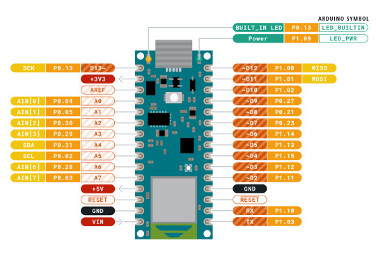
I wasn’t going to let this little bump in the road stop me from making use of bit parallelism. If you look carefully at the bit positions, the best continuous run we can get is 6 bits in a row with P1.10 through P1.15. It’s not possible to read the 8 data bits in one shot…or is it? If we connect D0/D1 of the camera to P1.02/P1.03 and D2-D7 to P1.10-P1.15, we can do a single 32-bit read from port P1 and get all 8 bits in one shot. The bits are in order, but will have a gap between D1 and D2 (P1.04 to P1.09). Luckily the Arm CPU has what’s called a barrel shifter. It also has a smart instruction set which allows data to be shifted ‘for free’ at the same time the instruction is doing something else. Let’s take a look at how and why I changed the code:
Original:
uint8_t in = 0; for (int k = 0; k < 8; k++) { bitWrite(in, k, (*_dataPorts[k] & _dataMasks[k]) != 0); }
Optimized:
uint32_t in = port->IN; // read all bits in parallel in >>= 2; // place bits 0 and 1 at the "bottom" of the register in &= 0x3f03; // isolate the 8 bits we care about in |= (in >> 6); // combine the upper 6 and lower 2 bits
Code analysis
If you’re not interested in the nitty gritty details of the code changes I made, you can skip this section and go right to the results below.First, let’s look at what the original code did. When I first looked at it, I didn’t recognize bitWrite; apparently it’s not a well known Arduino bit manipulation macro; it’s defined as:
#define bitWrite(value, bit, bitvalue) (bitvalue ? bitSet(value, bit) : bitClear(value, bit))
This macro was written with the intention of being used on GPIO ports (the variable value) where the logical state of bitvalue would be turned into a single write of a 0 or 1 to the appropriate bit. It makes less sense to be used on a regular variable because it inserts a branch to switch between the two possible outcomes. For the task at hand, it’s not necessary to use bitClear() on the in variable since it’s already initialized to 0 before the start of each byte loop. A better choice would be:
if (*_dataPorts[k] & _dataMasks[k]) in |= (1 << k);
The arrays _dataPorts[] and _dataMasks[] contain the memory mapped GPIO port addresses and bit masks to directly access the GPIO pins (bypassing digitalRead). So here’s a play-by-play of what the original code was doing:
Set in to 0
Set k to 0
Read the address of the GPIO port from _dataPorts[] at index k
Read the bit mask of the GPIO port from _dataMasks[] at index k
Read 32-bit data from the GPIO port address
Logical AND the data with the mask
Shift 1 left by k bits to prepare for bitClear and bitSet
Compare the result of the AND to zero
Branch to bitSet() code if true or use bitClear() if false
bitClear or bitSet depending on the result
Increment loop variable k
Compare k to the constant value 8
Branch if less back to step 3
Repeat steps 3 through 13, 8 times
Store the byte in the data array (not shown above)
The new code does the following:
Read the 32-bit data from the GPIO port address
Shift it right by 2 bits
Logical AND (mask) the 8 bits we’re interested in
Shift and OR the results to form 8 continuous bits
Store the byte in the data array (not shown above)
Each of the steps listed above basically translates into a single Arm instruction. If we assume that each instruction takes roughly the same amount of time to execute (mostly true on Cortex-M), then old vs. new is 91 versus 5 instructions to capture each byte of camera data, an 18x improvement! If we’re capturing a QVGA frame (320x240x2 = 153600 bytes), that becomes many millions of extra instructions.
Results
The optimized byte capture code translates into 5 Arm instructions and allows the capture loop to now handle a setting of 5 FPS instead of 1 FPS. The FPS numbers don’t seem to be exact, but the original capture time (QVGA @ 1 FPS) was 1.5 seconds while the new capture time when set to 5 FPS is 0.393 seconds. I tested 10 FPS, but readFrame() doesn’t read the data correctly at that speed. I don’t have an oscilloscope handy to probe the signals to see why it’s failing. The code may be fast enough now (I think it is), but the sync signals may become too unstable at that speed. I’ll leave this as an exercise to the readers who have the equipment to see what happens to the signals at 10 FPS.
For the work I did on the OV767X library, I created a test fixture to make sure that the camera data was being received correctly. For ML/data processing applications, it’s not necessary to do this. The built-in camera test pattern can be used to confirm the integrity of the data by using a CRC32.
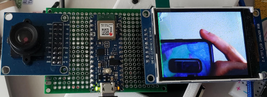
My tinned protoboard test fixture with 320×240 LCD
Note: The frames come one immediately after another. If you capture a frame and then do some processing and then try to capture another frame, you may hit the middle of the next frame when you call readFrame(). The code will then wait until the next VSync signal, so that frame’s capture time could be as much as 2x as long as a single frame time.
More tips
I enjoy testing the limits of embedded hardware, especially when it involves bits, bytes and pixels. I’ve written a few blog posts that explore the topics of speed and power usage if you’re interested in learning more about it.
Conclusion
The embedded microcontrollers available today are capable of handling jobs that were unimaginable just a few years ago.
Optimized ML solutions from Google and Edge Impulse are capable of running on low-cost, battery-powered boards (vision, vibration, audio, whatever sensor you want to monitor).
Python and Arduino programming environments can test your project idea with little effort.
Software can be written an infinite number of ways to accomplish the same task, but one constant remains: TANSTATFC (there ain’t no such thing as the fastest code).
Never assume the performance you’re seeing is what you’re stuck with. Think of existing libraries and generic APIs available through open source libraries and environments as a starting point.
Knowing a bit of info about the target platform can be helpful, but it’s not necessary to read the MCU datasheet. In the code above, the larger concept of Arm Cortex-M 32-bit GPIO ports was sufficient to accomplish the task without knowing the specifics of the nRF52’s I/O hardware.
Don’t be afraid to dig a little deeper and test every assumption.
If you encounter difficulties, the community is large and there are a ton of resources out there. Asking for help is a sign of strength, not weakness.
Optimizing a low-cost camera for machine vision was originally published on PlanetArduino
0 notes
Text
Lattice Semiconductor Launches New FPGA For Cyber-Resilient Systems
New Post has been published on https://perfectirishgifts.com/lattice-semiconductor-launches-new-fpga-for-cyber-resilient-systems/
Lattice Semiconductor Launches New FPGA For Cyber-Resilient Systems
Earlier this week, Lattice Semiconductor announced its newest product built on the Lattice Nexus FPGA platform, the Mach-NX. The Mach-NX FPGA product family addresses the growing threat of firmware hacking attempts on systems, leading to the loss of customer IP. Moor Insights & Strategy have written a lot about this growing threat, funded by nation-states with “as a service” business models.
As bad actors continue to attack firmware, companies like Lattice Semiconductor need to constantly be upping its games to enable their customers to create cyber-resilient systems. Enter a new FPGA from Lattice. The Mach-NX is a high performance, low power FPGA product family aimed at dynamic, real-time, and end-to-end platform protection. This launch is the next logical step for Lattice on its low power FPGA journey and marks the third Nexus launch in a year. The company is uniquely positioning itself as a leader, if not the leader in low power FPGA security solutions, and this launch helps reinforce that.
Lattice has been delivering new security-focused FPGAs at a faster cadence than we are used to. Since FPGAs are incredibly flexible, it also gives Lattice the ability to expand its presence into different markets that need programmable security solutions. In recent memory, Lattice launched CrossLink-NX in late 2019, Certus-NX this past summer, and now Mach-NX. You can read my full write up on the Certus-NX launch here. Lattice was ambitious when it promised to speed up its launch cadence by 3x, and it has done just that in 2020. The company seems hyper focused on low power FPGA dominance as 2020 comes to an end, and its future seems bright.
Lattice Semiconductor Mach NX
As hackers continue to attack firmware vulnerabilities with nation-state budgets and “as a service” models, companies need a flexible, secure solution that can adapt and serve different industries and applications. That problem is the exact reason that Lattice developed its new security-focused FPGA, Mach-NX. The new Mach-NX FPGA family will build on the previous product, the Lattice MachXO3D family. The new Mach-NX product family will address future server platforms, computing, communications, industrial, and automotive systems. Like other Lattice Nexus products, the new Mach-NX FPGA will utilize the same 28 nm FD-SOI fab process. While not a bleeding edge geometry, the specialized FD-SOI process technology allows Lattice to deliver extremely energy-efficient solutions without sacrificing performance. I also believe this solution is much smaller than competing solutions. High performance while maintaining low power matters a lot when you consider that traditionally high-density FPGAs trade power for size. I’ve talked enough about application and product introduction; let’s get into the nuts and bolts of the Mach-NX.
I listed the new features verbatim for the Mach-NX FPGA products from Lattice’s announcement.
Up to 8.4K LC of user logic, 2669kbits of user flash memory, and dual boot flash feature.
Up to 379 programmable I/O supporting 1.2/1.5/1.8/2.5/3.3 I/O voltages.
Secure enclave supports 384-bit cryptography, including SHA, HMAC, and ECC.
Lattice Semiconductor Mach-NX
The first goal of a security solution is establishing a Hardware Root of Trust upon boot, which the Mach-NX does. The Mach-NX FPGAs also give users real-time performance against security risks with real-time SPI monitoring. According to Lattice, the Mach-NX FPGAs can again recover firmware within microseconds, where other FPGAs can take 100s of milliseconds or even minutes to recover firmware.
The 384-bit encryption is a significant security upgrade from the 256-bit encryption we saw with the last generation products. This security level becomes essential, especially when considering the longevity of end products that would adopt the Mach-NX, which could be up to 10 years. As the number of attack vectors and cyber-attacks is increasing rapidly, security solutions need to adapt and become harder to hack. Another value that customers get from implementing Mach-NX FPGAs is customizing solutions specifically for their applications and use. Customers will be able to configure their FPGAs’ security using RISC-V and Lattice’s Propel Design Environment. I admire the way Lattice is positioning its Mach-NX solution as a first on, last-off, real-time, fully customizable solution for the customer’s unique needs. When you pair these solutions with Lattice’s security service, SupplyGuard, a customer’s system can be protected throughout the product life cycle’s duration.
Lattice Semiconductor Mach-NX
Wrapping up
All in all, Lattice’s new Mach-NX looks to deliver on its core value proposition and extends the capabilities of Lattice’s previous generation of secure control FPGAs. Attack vectors and hackers will continually evolve their attack methods, and as those change, I believe s Lattice’s solutions will volve to address those methods.
Since this time last year, Lattice has launched three FPGA product families built on its Lattice Nexus FPGA platform with no signs of slowing down. If you recall, since CEO Jim Anderson took the helm Lattice looks to have generated a tremendous amount of momentum with Lattice Nexus, as further reinforced by the launch of Mach-NX. Add to that the work the company has put in to round out its offerings with application-focused solutions stacks and software design tools, and it’s clear they are laser-focused on delivering on the promise of low power programmable leadership.
Note: Moor Insights & Strategy writers and editors may have contributed to this article.
Moor Insights & Strategy, like all research and analyst firms, provides or has provided paid research, analysis, advising, or consulting to many high-tech companies in the industry, including 8×8, Advanced Micro Devices, Amazon, Applied Micro, ARM, Aruba Networks, AT&T, AWS, A-10 Strategies, Bitfusion, Blaize, Box, Broadcom, Calix, Cisco Systems, Clear Software, Cloudera, Clumio, Cognitive Systems, CompuCom, Dell, Dell EMC, Dell Technologies, Diablo Technologies, Digital Optics, Dreamchain, Echelon, Ericsson, Extreme Networks, Flex, Foxconn, Frame (now VMware), Fujitsu, Gen Z Consortium, Glue Networks, GlobalFoundries, Google (Nest-Revolve), Google Cloud, HP Inc., Hewlett Packard Enterprise, Honeywell, Huawei Technologies, IBM, Ion VR, Inseego, Infosys, Intel, Interdigital, Jabil Circuit, Konica Minolta, Lattice Semiconductor, Lenovo, Linux Foundation, MapBox, Marvell, Mavenir, Marseille Inc, Mayfair Equity, Meraki (Cisco), Mesophere, Microsoft, Mojo Networks, National Instruments, NetApp, Nightwatch, NOKIA (Alcatel-Lucent), Nortek, Novumind, NVIDIA, Nuvia, ON Semiconductor, ONUG, OpenStack Foundation, Oracle, Poly, Panasas, Peraso, Pexip, Pixelworks, Plume Design, Poly, Portworx, Pure Storage, Qualcomm, Rackspace, Rambus, Rayvolt E-Bikes, Red Hat, Residio, Samsung Electronics, SAP, SAS, Scale Computing, Schneider Electric, Silver Peak, SONY, Springpath, Spirent, Splunk, Sprint, Stratus Technologies, Symantec, Synaptics, Syniverse, Synopsys, Tanium, TE Connectivity, TensTorrent, Tobii Technology, T-Mobile, Twitter, Unity Technologies, UiPath, Verizon Communications, Vidyo, VMware, Wave Computing, Wellsmith, Xilinx, Zebra, Zededa, and Zoho which may be cited in blogs and research.
From Cloud in Perfectirishgifts
0 notes