#Solar Panel PCB
Explore tagged Tumblr posts
Visit Tumblr Blog
Explore Tumblr blogs with no restrictions, modern design and the best experience.
Last Seen Tumblr Blogs


Fun Fact
Tumblr was created by web developers David Karp and Marco Arment.
Text
Skytron Energy CAN Protection PV18 PCB Card | Industrial PCB Module | Ram Automations
Explore high-performance industrial protection with the Skytron Energy CAN Protection PV18 PCB Card — a specialized PCB module crafted to ensure secure communication and safety for photovoltaic systems and energy control setups. Now available at Ram Automations, this tested, genuine Skytron Energy PCB card is perfect for engineers, OEM panel builders, and energy automation specialists looking to maintain the efficiency and reliability of solar power and industrial control networks.
The Skytron Energy CAN Protection PV18 is designed for CAN (Controller Area Network) communications, ensuring optimal protection, system longevity, and improved fault tolerance for critical energy systems. Whether you’re upgrading an industrial automation cabinet, servicing energy management units, or refurbishing solar monitoring systems, this PCB card is your go-to choice.
🛒 Product Link: https://ramautomations.com/products/skytron-energy-can-protection-pv18-pcb-card-used
🌐 Visit Our Website for More Automation Products: https://ramautomations.com
🔧 Product Overview
📦 Model: CAN Protection PV18
🏢 Brand: Skytron Energy
📌 Type: PCB Protection Card for CAN Networks
🆕 Condition: Tested, Verified
⚙️ Function: Signal Protection, CAN Bus Safeguarding, Energy Automation System Support
📍 Applications: Solar Plants, Energy Monitoring Systems, Industrial Automation Panels
✅ Key Features & Benefits
✔️ Genuine Skytron Energy PCB Card ✔️ Designed for critical CAN Bus communication ✔️ Optimized for energy control and monitoring systems ✔️ Enhances fault tolerance and system resilience ✔️ Ideal for solar and industrial automation ✔️ Compact, rugged, and highly efficient ✔️ Tested and reliable for long-term operations
🏭 Best Suited For
✔️ Solar Energy Plants ✔️ Energy Automation Systems ✔️ Industrial Automation Cabinets ✔️ CAN Network Controllers ✔️ Renewable Energy System Integrators ✔️ OEM Panel Upgrades ✔️ Industrial Retrofits
If you need a reliable replacement or a solid upgrade to maintain your energy automation system, the Skytron Energy CAN Protection PV18 PCB is the dependable solution you’ve been looking for.
🛠 Why Choose Ram Automations?
At Ram Automations, we specialize in providing genuine industrial and marine automation spare parts. Serving more than 1000+ global brands, we are your trusted partner for sourcing both current and legacy parts.
✔️ 1000+ Brands Available ✔️ Genuine, Tested Spare Parts ✔️ Fast Worldwide Shipping ✔️ OEM & Bulk Supply Support ✔️ Friendly Technical Assistance
📽️ In This Video You’ll Learn:
🔧 Full Visual Overview of the Skytron Energy PV18 CAN Protection PCB Card 🧰 Installation Tips for Energy Control Systems ⚡ Real-World Applications in Solar and Industrial Automation 📊 Importance of Reliable PCB Components in Energy Networks
📣 Subscribe to Ram Automations YouTube Channel for More! 💬 Drop your questions below — we’re here to help! 👍 Like the video if it helped you understand the product better 🔔 Subscribe for weekly uploads of rare automation spare parts and tutorials
#Skytron Energy CAN Protection PV18#Skytron PCB Card#Energy Automation PCB#Solar Panel PCB#CAN Protection Module#Solar Energy Automation#PCB for Solar Plants#Industrial Automation PCB#Energy Monitoring Components#Skytron Automation#Ram Automations#Automation Parts Supplier#Solar Control Board#Used Industrial PCB#Renewable Energy PCB Card#Automation Board#Industrial PCB Module#Energy Management Board#Solar Plant Monitoring PCB
2 notes
·
View notes
Text


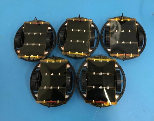
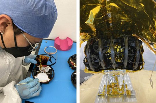
Colmena or "Hive" (2024) by Gustavo Medina Tanco plus a team of 200 students, from the National Autonomous University of Mexico (UNAM). This will be the first Mexican mission to the moon, carried aboard Astrobotic's Peregrine Lunar Lander launched on January 8th 2024, arriving on February 23rd. "The COLMENA Project, or “hive” in English, will involve a self-organized swarm of five robots, each weighing less than 60 grams and measuring just 12 centimeters in diameter, each equipped with a small solar panel. Inside the robots is a single, flexible PCB containing power conditioning, control, communications, monitoring, interface connector, arming and tripping, trip mechanism and grounding and bonding subsystems. The robots will autonomously navigate themselves to achieve electrical connectivity by joining their panels together to make a larger solar panel. The project will demonstrate how feasible it may be to build structures on planetary surfaces with robot swarms." – UNAM researchers to send micro-robots to the moon, The Robot Report, Brianna Wessling.
UPDATE: The Peregrine Lander began venting fuel soon after launch, making it difficult for Astrobotic to stabilise the spacecraft. The resulting loss of fuel means that it cannot attempt a moon landing.
20 notes
·
View notes
Text
Trump’s Tariff Hex: Chaos in the Electronics Forbidden Forest

In the labyrinthine alleys of Diagon Alley, where goblins mint golden semiconductors and owls ferry PCB blueprints, a dark enchantment has gripped the global electronics realm—the Trump Tariff Hex. Like a rogue spell from the Department of Mysteries, these levies threaten to splinter supply chains, ignite trade wars, and turn innovation into ash. Let us don our Invisibility Cloaks and unravel this cursed prophecy.
Chapter 1: The Dark Lord’s Trade Decree
The Trumpian Tariffius Maxima—a 10% baseline levy on imports, soaring to 25% for chips, EVs, and solar panels—has cast a shadow darker than a Dementor’s kiss. “Liberation Day,” they call it. But as economist Bala Ramasamy warns, “This is no liberation—it’s a Howler screeching trade deficits and shortages”.
Why this hex outshines Umbridge’s cruelty:
Chipmakers’ Horcrux Hunt: Semiconductors, the Philosopher’s Stones of tech, now face 25% tariffs. NVIDIA’s GPUs risk vanishing like a poorly cast Evanesco, forcing TSMC to build Arizona “Horcrux fabs” under Ministry (of Commerce) scrutiny.
Solar Panels & the Phoenix Protocol: China’s solar giants, exiled by decade-old tariffs, rise anew in Southeast Asia—burning U.S. tariffs to ash like Fawkes reborn.
Chapter 2: The Triwizard Tournament of Trade Wars
1. The Hungarian Horntail (U.S. vs. China): China retaliates with Confringo tariffs on coal, LNG, and EVs, igniting a duel where both sides lose. Yet, Chinese solar firms—commanding 80% of global production—Apparate supply chains to Cambodia and Vietnam, leaving U.S. tariffs chasing ghosts.
2. The Maze of Supply Chains (Automakers’ Plight): Tesla’s Shanghai Gigafactory, once a golden snitch of profit, now stings under 20% tariffs. Ford’s electric dreams crumble as battery costs soar 15%, cursed by Inflatus pricing spells.
3. The Goblet of Fire (Stock Market Inferno): The “Magnificent Seven” tech titans—Apple, NVIDIA, Tesla—plummet like Bludgers hit by tariff jinxes. Nasdaq’s 4.5% drop mirrors a shattered Protego charm, as investors flee to Gringotts gold.

Chapter 3: The Prophecies of Tech Seers
Sybill Trelawney’s Grim Forecast:
Short-Term: Capacitors, resistors, and sensors rise 10-15% in price—faster than a Snitch evades capture.
Long-Term: A fragmented global market where “Made in USA” labels are as rare as a Hufflepuff in Slytherin.
Dumbledore’s Whispered Wisdom: “Dark tariffs feed on fear. But remember, the Phoenix of Adaptation always rises—if we dare to let it.”
The Counter-Charm: Brewing the Antidote
1. The ASEAN Portkey: Factories flee to Vietnam, Malaysia, and Thailand—safe havens where tariff Dementors cannot feast. 2. The Alchemy of Localization: TSMC’s Arizona fabs and Tesla’s Berlin Gigafactory mutter Protego Profitabilis!, shielding margins with localized production. 3. The Patronus of Innovation: Startups weave tariff-resistant spells—modular designs, 3D-printed PCBs, and AI-driven logistics owls.
Epilogue: A Wizard’s Choice The electronics realm stands at a crossroads: succumb to the tariff hex or wield the Elder Wand of diversification. As Harvey Dzodin, a sage of Muggle policy, cautions: “This path leads to stagflation—a Dementor’s kiss for progress.” Yet, like Harry’s defiant Expecto Patronum, the industry may yet dispel the darkness… one agile incantation at a time.
References
The Dark Arts of Global Trade (Ministry of Economics, 2025)
Solar Phoenix: Escaping the Tariff Labyrinth (Hogwarts Press)
NASDAQ’s Fall: A Cauldron of Investor Tears (Daily Prophet Finance)
1 note
·
View note
Text
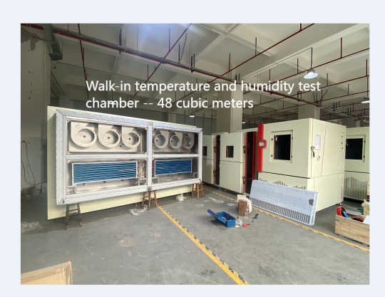
Walk-in environmental test chamber: The perfect solution for your experimental needs!
JOEO walk in environmental chamber is used to test full-size solar panels or other large products Performance tomeet IEC 61215, 61646, UL-1703 and similar test requirements, Widely used in industries such as electronic products, PCBs, semiconductors, automobiles, aerospace, etc
#ReliabilityTesting#InnovationInElectronics#temperaturechamber#EnvironmentalChamber#walkinchamber#batterytesting#aerospacetechnology#JOEOtestingchamber
2 notes
·
View notes
Text
Electronics & PCB Industry Driving Copper Foil Demand
The global copper foil market is on an upward trajectory, driven by the increasing need for efficient and high-performance conductive materials. With the growing adoption of electric vehicles (EVs), flexible printed circuits, and lithium-ion batteries, copper foil has become a critical component in various industries. By 2035, the market is expected to reach USD 16,580.1 million, growing at a CAGR of 7.8%.
The market's expansion is largely fueled by the rising demand for copper foil in energy storage solutions and 5G infrastructure. The increasing focus on sustainability and recyclable materials is further shaping the industry's growth landscape.
Get Ahead with Our Report: Request Your Sample Now! https://www.futuremarketinsights.com/reports/sample/REP-GB-12399
Market Growth Drivers
Growing EV Battery Production – Lithium-ion battery manufacturers increasingly rely on high-purity copper foil for enhanced conductivity and efficiency.
Expanding Electronics and PCB Sector – The proliferation of smart devices and high-speed computing systems is pushing demand for advanced copper foils.
Technological Advancements – Innovations in ultra-thin and electrodeposited copper foil manufacturing enhance product quality and application scope.
Rising Investments in Renewable Energy – Solar panels and wind energy storage systems are driving additional demand for copper foil.
Sustainability Focus – Market players are integrating green production processes to meet environmental regulations.
Key Advancements in Copper Foil Manufacturing Processes
Innovations in electrodeposition techniques and high-precision rolling have enabled manufacturers to produce thinner, more conductive, and high-performance copper foils. These advancements are critical for their application in lithium-ion batteries, 5G circuits, and high-frequency PCBs. Sustainable production methods, including copper recycling and low-emission manufacturing processes, are also gaining momentum.
"The copper foil market is experiencing strong growth, driven by rising demand in EV batteries, PCBs, and renewable energy. Key players are focusing on advanced manufacturing techniques and sustainability to maintain a competitive edge," says Nikhil Kaitwade, Associate Vice President at Future Market Insights (FMI).
Key Takeaways from Copper Foil Market Study
The market will witness a CAGR of 7.8% from 2025 to 2035.
EV battery and electronics sectors are the largest consumers of copper foil.
Asia-Pacific leads the market, driven by strong production bases in China, Japan, and South Korea.
Ultra-thin and high-purity copper foil demand is increasing for next-gen applications.
Sustainable manufacturing practices and recycling innovations are gaining traction.
Exhaustive Market Report: A Complete Study! https://www.futuremarketinsights.com/reports/copper-foil-market
Key Market Trends Influencing Competitive Dynamics
Expansion in EV Battery Production: Leading companies are investing heavily in new manufacturing plants and expanding production capacities to support the increasing demand for lithium-ion batteries in electric vehicles.
Technological Advancements in Copper Foil Production: Innovations in ultra-thin and electrodeposited copper foils are enabling superior performance in electronics and energy storage applications.
Sustainability and Recycling Initiatives: Companies are focusing on sustainable production methods and efficient copper recycling to align with global environmental standards.
Regional Market Penetration Strategies: Asia-Pacific continues to dominate the copper foil market, with companies expanding operations in China, South Korea, and Japan, while North America and Europe are witnessing increased investments in local production to reduce supply chain dependencies.
Key Companies and Market Share Insights
The global copper foil market is characterized by the presence of several key players who are leading the industry through innovation, strategic investments, and expansions. With increasing demand for copper foil across multiple industries, including electric vehicles (EVs), printed circuit boards (PCBs), and energy storage solutions, major companies are focusing on product differentiation, sustainability, and technological advancements.
1. Mitsui Mining & Smelting Co., Ltd.
Market Position: One of the leading producers of high-performance copper foils for the electronics and EV industries.
Strategic Focus: Mitsui has been heavily investing in expanding its production capacity to cater to the rising demand for ultra-thin copper foils used in lithium-ion batteries.
Recent Developments: The company has announced plans to enhance its production efficiency by integrating advanced electrodeposition techniques to improve foil conductivity and durability.
2. Furukawa Electric Co., Ltd.
Market Position: A key supplier of copper foils for flexible printed circuits (FPCs), telecommunications, and next-generation semiconductor applications.
Strategic Focus: The company is focusing on developing ultra-thin and high-purity copper foils to support the growing demand in the 5G and IoT markets.
Recent Developments: Furukawa has introduced new copper foil solutions that enhance thermal and electrical performance, enabling their use in high-frequency PCBs and next-generation electronic devices.
3. JX Nippon Mining & Metals Corporation
Market Position: A dominant player in the production of electrodeposited copper foil for energy storage and electronic applications.
Strategic Focus: The company is investing in R&D for sustainable and recyclable copper foil solutions, aiming to reduce environmental impact while maintaining high-performance standards.
Recent Developments: JX Nippon has announced advancements in copper foil recycling, ensuring greater material efficiency and aligning with global sustainability initiatives.
4. Doosan Corporation
Market Position: A global leader in supplying copper foils for lithium-ion batteries, particularly for EV and energy storage systems.
Strategic Focus: The company is focusing on enhancing its copper foil production to cater to the growing EV battery market, particularly in North America and Europe.
Recent Developments: Doosan has invested in new production facilities to meet increasing demand and has introduced thinner, more conductive copper foil options to improve battery efficiency.
5. Circuit Foil Luxembourg
Market Position: A specialized manufacturer of copper foils used in PCBs, high-frequency circuits, and advanced microelectronics.
Strategic Focus: The company aims to expand its global reach and improve the durability and flexibility of its copper foils to support the growing miniaturization trend in electronics.
Recent Developments: Circuit Foil has developed ultra-thin, high-durability foils specifically designed for applications requiring superior thermal and electrical conductivity.
These companies are actively expanding their production capacities, investing in R&D, and forming strategic partnerships to strengthen their market positions.
Recent Developments in the Copper Foil Industry
Mitsui Mining & Smelting recently expanded its production capacity to cater to rising EV battery demand.
Furukawa Electric announced breakthroughs in ultra-thin copper foil technology for flexible circuits.
JX Nippon Mining & Metals introduced a new sustainable copper foil recycling process to support environmental goals.
Doosan Corporation is developing high-performance copper foils tailored for 5G applications.
About Future Market Insights (FMI)
Future Market Insights, Inc. (ESOMAR certified, recipient of the Stevie Award, and a member of the Greater New York Chamber of Commerce) offers profound insights into the driving factors that are boosting demand in the market. FMI stands as the leading global provider of market intelligence, advisory services, consulting, and events for the Packaging, Food and Beverage, Consumer Technology, Healthcare, Industrial, and Chemicals markets. With a vast team of over 400 analysts worldwide, FMI provides global, regional, and local expertise on diverse domains and industry trends across more than 110 countries.
Join us as we commemorate 10 years of delivering trusted market insights. Reflecting on a decade of achievements, we continue to lead with integrity, innovation, and expertise.
Contact Us:
Future Market Insights Inc. Christiana Corporate, 200 Continental Drive, Suite 401, Newark, Delaware – 19713, USA T: +1-347-918-3531 For Sales Enquiries: [email protected] Website: https://www.futuremarketinsights.com LinkedIn| Twitter| Blogs | YouTube
0 notes
Text
Leading Copper Strips Manufacturers in India – Superior Performance & Reliability by KWM India
Copper is one of the most important metals in industrial and electrical applications, thanks to its outstanding electrical conductivity, thermal efficiency, corrosion resistance, and malleability. Among its many forms, copper strips are a widely used product, favored across industries such as power distribution, electronics, telecommunications, renewable energy, and manufacturing. As one of the top copper strips manufacturers in India, KWM India offers precision-engineered copper strips that meet global quality standards, customized to meet diverse industry requirements.
What Are Copper Strips?
Copper strips are long, narrow, flat pieces of copper produced by rolling copper slabs or billets into thin, continuous forms. These strips are manufactured in various thicknesses, widths, and tempers to suit different applications. Their superior conductivity, excellent resistance to corrosion, and high strength make them ideal for use in both electrical and mechanical systems.
Whether it’s a power transmission project, electrical control system, or a grounding network, copper strips play a vital role in ensuring reliable, efficient, and safe operations.
KWM India – A Trusted Manufacturer of Copper Strips
KWM India has become a recognized name in the Indian non-ferrous metals industry, known for its advanced manufacturing facilities, experienced workforce, and unwavering commitment to quality. As a prominent copper strips manufacturer in India, KWM serves a wide range of sectors, offering copper products that deliver consistent performance, durability, and precision.
By focusing on innovation and customer satisfaction, KWM India ensures that its copper strips are produced to meet the technical specifications and compliance standards required by modern industry.
Key Features of Copper Strips by KWM India:
High-Purity Electrolytic Copper: KWM uses top-grade copper (up to 99.9% purity) to manufacture strips with superior electrical and thermal conductivity.
Customized Dimensions & Tempers: Copper strips are available in a range of thicknesses (0.2 mm to 6 mm), widths, and tempers (soft, half-hard, and hard), tailored to client needs.
Tight Tolerances & Accuracy: KWM employs advanced rolling mills and cutting equipment to maintain dimensional precision and surface uniformity.
Corrosion Resistance: KWM’s copper strips are ideal for indoor and outdoor applications, including humid or chemically active environments.
Surface Finish & Quality Assurance: Products feature a smooth finish with minimal surface oxidation. Every batch undergoes rigorous testing to ensure quality, strength, and consistency.
Applications of Copper Strips
KWM India’s copper strips are used across a wide array of industries:
Electrical Industry: Extensively used in busbars, switchgear, control panels, connectors, terminals, and grounding systems due to their unmatched conductivity.
Power Generation & Distribution: Applied in transformers, circuit breakers, and substation components for efficient energy transmission.
Renewable Energy: Used in solar panels, inverters, and wind turbine systems for reliable and eco-friendly power solutions.
Electronics & Telecommunications: Employed in printed circuit boards (PCBs), antennas, and shielding applications.
Industrial Machinery: Utilized in heat exchangers, welding equipment, and mechanical parts where strength and conductivity are essential.
Automotive & Railways: Copper strips are used in EV components, electrical wiring systems, and connectors.
Why Choose KWM India?
Experience & Expertise: With years of experience in copper product manufacturing, KWM understands the complex needs of various industries and delivers accordingly.
Technological Advantage: KWM’s advanced rolling and quality control systems ensure each product meets precise technical and functional specifications.
Customized Solutions: From small orders to large-scale industrial supply, KWM offers flexible production and delivery options tailored to your requirements.
Quality Certifications: All products are manufactured following ISO standards and meet national and international quality norms.
Efficient Logistics: A robust distribution network ensures timely delivery across India and to global clients.
Sustainability Commitment: KWM uses eco-friendly processes and recycles materials wherever possible, contributing to greener manufacturing.
Conclusion
As industries across the globe evolve with increasing reliance on efficient and sustainable electrical systems, the demand for high-quality copper strips continues to rise. KWM India, as one of the premier copper strips manufacturers in India, meets this demand with products that combine performance, durability, and precision.
Whether you're looking for standard copper strips or need customized dimensions and properties, KWM India is your trusted partner for excellence in copper manufacturing.
Contact KWM India today to request a quote or learn more about their copper strip solutions designed for modern industry needs.
Visit:- https://www.kmwindia.com/copper-strips.html
0 notes
Text
How many types of solder bars are there?
Solder bars play a crucial role in metal joining applications across various industries — from electronics and automotive to plumbing and electrical assembly. Despite being small in size, the type of solder bar you choose can significantly impact the strength, conductivity, and reliability of the joint.
So, how many types of solder bars are there? The answer depends on composition, application, and whether the bar is lead-based or lead-free.
Let’s take a closer look.
🔹 1. Tin-Lead Solder Bars (Sn-Pb)
This is the most traditional type of solder bar, commonly used in the past across many industries. It consists primarily of tin (Sn) and lead (Pb), and is available in different ratios.
Common Ratios:
60/40 (60% Tin, 40% Lead)
63/37 (Eutectic alloy) – Offers a sharp melting point at 183°C, which makes soldering faster and cleaner.
Advantages:
Smooth flow and excellent wettability
Strong, reliable joints
Cost-effective
Disadvantages:
Not environmentally friendly (due to lead content)
Restricted in many countries due to health and safety regulations (e.g., RoHS)
Best for: Legacy systems, industrial applications where RoHS compliance is not required.
🌿 2. Lead-Free Solder Bars
With global regulations pushing for safer, non-toxic materials, lead-free solder bars have become the industry standard in consumer electronics and industrial manufacturing.
These bars contain tin as the base metal, alloyed with other metals like copper, silver, or bismuth.
Common Lead-Free Compositions:
SAC305 – Tin (96.5%), Silver (3%), Copper (0.5%)
Sn-Cu – Tin (99.3%), Copper (0.7%)
Sn-Bi – Tin and Bismuth (used for low-temperature applications)
Advantages:
Environmentally safe and RoHS compliant
Good mechanical strength and thermal stability
Excellent for high-reliability applications
Disadvantages:
Higher melting points compared to leaded solder
Can be more expensive due to silver content
Best for: Electronics, consumer products, automotive, medical devices.
🧪 3. Specialty Solder Bars
These solder bars are designed for specific industrial requirements and may have unique alloy compositions or surface treatments to enhance performance.
Examples Include:
High-Silver Solder Bars – Provide excellent conductivity and joint strength; used in aerospace, defense, and precision electronics
Low-Residue Solder Bars – Leave minimal flux residue; ideal for cleanroom environments
Antioxidation Coated Solder Bars – Prevent surface oxidation during storage and reflow processes
Advantages:
Tailored for niche applications
Improved long-term performance
Consistent quality under challenging environments
Best for: Aerospace, solar panels, military-grade electronics, medical instruments.
📌 Summary Table
Solder Bar TypeMain CompositionRoHS CompliantApplicationTin-Lead (Sn-Pb)Tin + Lead❌Traditional soldering, legacy equipmentSAC305Tin + Silver + Copper✅General electronics, SMT assemblySn-CuTin + Copper✅Electrical wiring, plumbingSn-BiTin + Bismuth✅Low-temp applications, sensitive componentsSpecialty BarsVaries (Silver-rich, coated)✅High-reliability industries
🔧 Choosing the Right Solder Bar
The ideal solder bar for your process depends on:
Required melting temperature
Mechanical and electrical performance needs
Regulatory compliance (e.g., lead-free requirements)
Environmental conditions of the application
Compatibility with automated or manual soldering systems
🏭 Hiflo Solders – Trusted Manufacturer of Quality Solder Bars
At Hiflo Solders, we manufacture a full range of:
Tin-Lead Solder Bars
Lead-Free Solder Bars (SAC, Sn-Cu, Sn-Bi)
Specialty Custom Alloys
Solder products designed for optimal flow, strength, and conductivity
With decades of expertise and a commitment to quality, our products are widely used in PCB assembly, electrical manufacturing, and industrial soldering lines.
🔗 For professional-grade soldering results, choose the right alloy — choose Hiflo.
📩 Interested in bulk orders or custom formulations? Contact our technical team today!
#SolderBars#HifloSolders#LeadFreeSolder#SnPb#SAC305#ElectronicsManufacturing#PCBAssembly#SolderingSolutions#EngineeringMaterials#ManufacturingInnovation#IndustrialSoldering#MetalAlloys#SmartSoldering
0 notes
Text
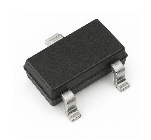
What Is an NPN Bipolar Transistor and Why Does It Matter?
The world of electronics thrives on components that serve both basic and complex functions, and one such foundational element is the NPN Bipolar Transistor. Known for its wide range of applications and efficient current control capabilities, this component is found in everything from microcontrollers to power tools, laptops, and safety circuits. Whether you're working with controllers, connectors, or sensors, understanding how an NPN Bipolar transistor works can significantly enhance your electronic project outcomes.
How Does an NPN Bipolar Transistor Work?
Before diving into its uses, it's important to grasp the operational principle behind this device. An NPN transistor belongs to the Bipolar Junction Transistor (BJT) family. It comprises three layers: the emitter, base, and collector.
The structure allows current to flow from the collector to the emitter when a small current is applied to the base. In simple terms, it amplifies or switches electrical signals. Due to its efficient operation, it is widely utilized in microprocessors, LED circuits, and signal amplifiers across industries.
Key Features of NPN Transistors
NPN bipolar transistors are favored for several reasons, including:
Higher electron mobility, which makes them faster than PNP types
Compatible with positive ground systems
Require a smaller base current for switching
Provide high gain and low saturation voltage
Suitable for fast switching in controllers and logic gates
Benefits of Using NPN Bipolar Transistors
Adding an NPN transistor to your circuit design offers tangible advantages. First and foremost, it improves the efficiency and control of your electrical load, making it a top choice in switches, thermal controls, and smart devices.
In addition:
They are compact and cost-effective for mass production
Ideal for circuits requiring fast response time
Provide better heat dissipation with thermal pads or oils
Enhance durability in tools, grips, and portable electronics
Deliver consistent performance in varying thermal conditions
Typical Applications of NPN Bipolar Transistors
The adaptability of this transistor type extends across industries. Whether in home automation or industrial machinery, its presence ensures stability and accuracy. Here are some popular use cases:
Signal amplification in audio devices, speakers, and LEDs
Switching applications in fuses, safety sensors, and contactors
Voltage regulation in laptop chargers, battery packs, and solar panels
Control systems for robotics, drones, and automation equipment
Pulse generation in oscillators, timers, and controllers
Interface bridging in connectors, PCBs, and cables
Role in Thermal and Safety Systems
In modern electronics, thermal management and safety assurance are crucial. NPN transistors work seamlessly with thermal sensors, thermal pads, and cooling fans to regulate temperature in circuits. Additionally, their role in preventing electrical overloads contributes to circuit longevity and operator safety.
Compatibility with Other Electronic Components
One of the standout traits of NPN transistors is how easily they integrate with a variety of other electronic components:
Work alongside capacitors to manage voltage fluctuations
Paired with microcontrollers to execute decision-making in smart systems
Help activate relays, contactors, and power regulators
Aid in signal processing within communication tools and sensors
Furthermore, NPN transistors are extensively used in IoT devices, wearables, and embedded systems, which often rely on microprocessors and LED indicators to provide feedback and automation.

Design Considerations When Using NPN Transistors
When incorporating NPN transistors into your circuit design, a few important aspects should be kept in mind:
Ensure correct pin configuration (emitter, base, collector)
Apply proper biasing to avoid circuit malfunction
Combine with thermal pads or heatsinks if used in high-power applications
Integrate with grips, tools, or safety enclosures for user protection
Select appropriate switches and fuses to safeguard against short circuits
Why Engineers and Hobbyists Rely on NPN Transistors
From DIY projects to industrial prototypes, the NPN transistor is a go-to choice for its simplicity and versatility. With the increasing demand for smart electronics, wireless controllers, and efficient sensors, NPN transistors continue to play a pivotal role in circuit design.
These transistors are also ideal for learning environments. Electronics students and hobbyists often start with basic NPN switching circuits before progressing to advanced systems involving microcontrollers, LED displays, and safety circuits.
Conclusion: A Must-Have Component in Every Electronics Toolkit
To sum up, the NPN Bipolar Transistor is more than just a switch or amplifier. It’s a vital element of modern electronics, powering everything from thermal systems and controllers to connectors and capacitors. Thanks to its affordability, efficiency, and compatibility with other devices such as laptops, tools, and microprocessors, it's an essential component for anyone serious about building reliable, high-performance electronics.
For those seeking a balance of performance, cost, and integration ease, choosing NPN transistors makes practical sense. Whether you're working on industrial controllers, robotic arms, or a basic LED blinking circuit, these transistors provide the support and stability your system demands.
0 notes
Text
Bonding Metal Wire Market - Business Outlook and Innovative Trends | New Developments, Current Growth Status, Emerging Opportunities, Upcoming Products Demand
Global Bonding Metal Wire Market Research Report 2025(Status and Outlook)
The global Bonding Metal Wire Market size was valued at US$ 1.84 billion in 2024 and is projected to reach US$ 2.73 billion by 2032, at a CAGR of 5.47% during the forecast period 2025-2032.
Bonding metal wires are ultra-thin metallic filaments used to create electrical interconnections in semiconductor packaging. These wires primarily consist of gold, aluminum, or copper materials and serve as conductive pathways between integrated circuit chips and their packaging substrates. The three dominant wire types include gold bonding wires (offering superior conductivity but higher cost), copper bonding wires (cost-effective with good thermal properties), and aluminum bonding wires (lightweight with excellent oxidation resistance).
The market growth is primarily driven by expanding semiconductor production, particularly in Asia-Pacific regions where countries like China, South Korea, and Taiwan dominate chip manufacturing. However, copper wire adoption faces challenges due to oxidation risks and specialized equipment requirements. Recent advancements include palladium-coated copper wires gaining traction for improved reliability. Key players like Heraeus and Tanaka are investing in R&D to develop advanced alloys that balance performance and cost-efficiency in response to evolving packaging technologies.
Our comprehensive Market report is ready with the latest trends, growth opportunities, and strategic analysis. https://semiconductorinsight.com/download-sample-report/?product_id=95877
Segment Analysis:
By Type
Copper Bonding Wires Dominate Due to Superior Electrical Conductivity and Cost Efficiency
The market is segmented based on type into:
Aluminum Bonding Wires
Subtypes: Ultra-thin aluminum wires, standard aluminum bonding wires
Copper Bonding Wires
Subtypes: Bare copper wires, coated copper wires
Gold Bonding Wires
Silver Bonding Wires
Others
By Application
Semiconductor Packaging Leads Demand Owing to Expanding Electronics Manufacturing
The market is segmented based on application into:
Semiconductor Packaging
PCB Assembly
Solar Panel Manufacturing
LED Packaging
Others
By Wire Diameter
Fine-Diameter Wires Hold Significant Share for Precision Interconnection Needs
The market is segmented based on wire diameter into:
Ultra-fine (<25μm)
Fine (25-50μm)
Standard (50-100μm)
Thick (>100μm)
By Bonding Method
Thermosonic Bonding Gains Preference for Reliable Interconnections in Advanced Packages
The market is segmented based on bonding method into:
Thermocompression Bonding
Thermosonic Bonding
Ultrasonic Bonding
Others
Regional Analysis: Metal Wire Market
North America North America represents a mature yet innovation-driven market for bonding metal wires, primarily fueled by the semiconductor and advanced electronics sectors. The U.S. accounts for approximately 38% of regional demand, supported by substantial R&D investments in semiconductor packaging technologies. Copper bonding wires are gaining traction due to their cost advantages over gold, though gold remains prevalent in high-reliability applications like aerospace and medical devices. Regulatory pressures related to material safety drive the adoption of eco-friendly alternatives, while the reshoring of electronics manufacturing under initiatives like the CHIPS Act presents growth opportunities. However, high labor costs and competitive pricing from Asian suppliers restrain market expansion.
Europe Europe’s market is characterized by stringent EU regulations on materials (e.g., RoHS directives) and a strong emphasis on precision engineering. Germany and the UK lead in demand, driven by automotive electronics and industrial automation sectors. The region is transitioning toward copper and palladium-coated wires to reduce dependency on gold, aligning with sustainability goals. While technological expertise remains high, slower growth in semiconductor production compared to Asia-Pacific limits volume expansion. Collaborative research between wire manufacturers and academic institutions, particularly in wafer-level packaging, is fostering niche innovations.
Asia-Pacific Dominating over 60% of global consumption, Asia-Pacific thrives due to concentrated semiconductor fabrication hubs in Taiwan, South Korea, and China. China’s aggressive investments in domestic chip production (e.g., $150 billion allocated under the “Made in China 2025” initiative) propel demand for cost-effective aluminum and copper wires. India and Southeast Asia are emerging hotspots, with PCB and consumer electronics manufacturing shifting to these regions. Price sensitivity favors local suppliers like MK Electron, though quality inconsistencies in low-tier products persist. The region’s rapid adoption of 5G and IoT devices further expands application scope.
South America The market remains nascent, with Brazil serving as the primary demand center for bonding wires used in automotive and consumer electronics assembly. Limited local semiconductor production restricts growth, with most wires imported from Asia or North America. Economic instability and currency fluctuations deter large-scale investments, though Mexico’s proximity to the U.S. supply chains offers modest opportunities. Copper wire adoption is slowly rising due to cost benefits, but gold retains dominance in legacy systems. Infrastructure gaps in technical training and testing facilities hinder market maturation.
Middle East & Africa This region exhibits the lowest market share but shows potential in semiconductor packaging for oil/gas sensors and telecommunications infrastructure. The UAE and Saudi Arabia lead with FDI-driven industrial diversification plans, while South Africa’s automotive sector utilizes bonding wires for electronic components. Dependence on imports and lack of localized R&D cap growth. However, partnerships with Asian wire manufacturers to establish distribution hubs could gradually improve accessibility. The focus remains on basic applications, with premium materials like gold used sparingly in niche segments.
List of Key Metal Wire Companies Profiled
Heraeus (Germany)
Tanaka Holdings (Japan)
Sumitomo Metal Mining (Japan)
MK Electron (South Korea)
AMETEK (U.S.)
Doublink Solders (U.S.)
Yantai Zhaojin Kanfort (China)
Tatsuta Electric Wire & Cable (Japan)
Kangqiang Electronics (China)
The Prince & Izant (U.S.)
The global semiconductor industry’s rapid growth is significantly driving demand for bonding metal wires, with semiconductor packaging accounting for over 75% of total wire bonding applications. As chip manufacturers race to meet demands from 5G, IoT, and AI applications, production volumes have increased by approximately 18% year-over-year, directly correlating with higher consumption of bonding wires. The transition to advanced packaging technologies like fan-out wafer-level packaging (FO-WLP) and 3D IC stacking requires more sophisticated wire bonding solutions, creating additional market opportunities for high-performance bonding wires.
Copper bonding wires are gaining substantial market share, currently representing about 35% of global bonding wire shipments, driven by their cost-effectiveness and superior electrical conductivity compared to traditional gold wires. The automotive electronics sector particularly favors copper wires for their reliability in high-temperature environments, with adoption rates growing at 12% annually. Major manufacturers are aggressively expanding copper wire production capacity to meet this demand, with several Asian producers increasing output by 20-25% in recent fiscal years.
The relentless push for smaller, more powerful electronic devices is forcing packaging innovations that require ultra-fine bonding wires. Demand for wires with diameters below 20μm has grown by 30% in the past three years, particularly in mobile device applications. This trend is driving significant R&D investments in wire bonding technologies, with leading manufacturers allocating 8-10% of revenues to develop next-generation bonding solutions capable of supporting finer pitches and higher Input/Output densities.
The automotive semiconductor market’s projected annual growth rate of 12% through 2030 presents significant opportunities for bonding wire manufacturers. Advanced driver assistance systems (ADAS) and vehicle electrification require specialized bonding solutions capable of withstanding harsh operating conditions. Manufacturers developing alloy wires with enhanced thermal and mechanical properties are capturing this high-margin segment, with some reporting 30% higher ASPs compared to standard bonding wires.
Southeast Asia’s semiconductor packaging industry is expanding rapidly, with new facility investments growing by 25% annually. This geographic shift in production is prompting bonding wire manufacturers to establish local operations, reducing logistics costs and improving customer responsiveness. Several leading producers have announced capacity expansions in Malaysia, Vietnam, and Thailand, with projected output increases of 40-50% over the next five years to serve these growing regional markets.
Development of novel bonding wire alloys combining gold, palladium, and copper is enabling performance improvements in critical applications. These premium products command 50-70% price premiums over standard wires and are gaining traction in medical devices and aerospace electronics. Material science breakthroughs in wire surface treatments and dopants are further enhancing reliability, opening doors to applications requiring ultra-long product lifespans under extreme conditions.
The market is highly fragmented, with a mix of global and regional players competing for market share. To Learn More About the Global Trends Impacting the Future of Top 10 Companies https://semiconductorinsight.com/download-sample-report/?product_id=95877
Key Questions Answered by the Bonding Metal Wire Market Report:
What is the current market size of Global Bonding Metal Wire Market?
Which key companies operate in Global Bonding Metal Wire Market?
What are the key growth drivers?
Which region dominates the market?
What are the emerging trends?
Browse More Reports:
CONTACT US:
City vista, 203A, Fountain Road, Ashoka Nagar, Kharadi, Pune, Maharashtra 411014
[+91 8087992013]
0 notes
Text
Functional Printing Market Size, Strategic Trends, End-Use Applications
The functional printing market was valued at USD 11.2 billion in 2022 and is anticipated to reach USD 35.1 billion by 2030, growing at a CAGR of 16.5% during the forecast period. The rapid evolution of printed electronics, combined with increasing adoption in packaging, automotive, and wearable technologies, is driving global demand.
Overview
Functional printing refers to the use of printing technology to create electronic components and devices on a variety of substrates, such as plastic, glass, and paper. Unlike conventional printing, which is used primarily for visual appeal, functional printing serves a technical purpose, enabling functionalities like conductivity, sensing, and energy storage.
With developments in materials science, nanotechnology, and ink formulation, functional printing is gaining traction in a wide range of industries. Applications include RFID tags, sensors, photovoltaic cells, displays, smart labels, and medical devices. Its cost-effectiveness, flexibility, and scalability make it a disruptive alternative to traditional manufacturing techniques in the electronics space.
Market Segmentation
By Technology
Inkjet Printing
Screen Printing
Flexographic Printing
Gravure Printing
Offset Printing
By Material
Substrates (Glass, Plastic, Paper)
Functional Inks (Conductive Inks, Dielectric Inks, Biodegradable Inks)
By Application
RFID Tags
OLED Displays
Sensors
Batteries
Photovoltaic Cells
Printed Circuit Boards (PCBs)
Smart Packaging
By End-User Industry
Automotive
Consumer Electronics
Healthcare
Retail
Energy
Industrial Manufacturing
Key Trends
Rapid growth of printed electronics in consumer and industrial IoT applications
Rising demand for flexible and lightweight devices in wearables and smart textiles
Emergence of bio-compatible printed sensors for health monitoring and diagnostics
Sustainable innovation with biodegradable inks and recyclable substrates
Integration with additive manufacturing for cost-efficient, large-scale production
Segment Insights
Technology Insights: Inkjet and screen printing technologies dominate the functional printing landscape due to their compatibility with a wide variety of functional inks and substrates. Inkjet printing offers high-resolution output and is ideal for small-scale production and prototyping, while screen printing provides high-throughput capabilities for commercial-scale runs.
Material Insights: The selection of functional inks plays a critical role in the performance of printed components. Conductive inks (silver-based or carbon-based) are commonly used for circuit printing, while dielectric and piezoelectric inks are utilized in sensors and capacitors. Flexible substrates enable printing on irregular surfaces, contributing to the growth of wearable and curved-display technologies.
Application Insights: RFID and smart packaging are among the most mature applications, widely adopted in logistics, retail, and food tracking. The market is now seeing accelerated growth in printed batteries, solar cells, and biosensors, as these solutions become more commercially viable and performance-efficient.
End-User Insights
Automotive: Utilizes functional printing for touch panels, lighting elements, in-vehicle sensors, and heated mirrors. Lightweight, flexible printed components improve energy efficiency and design adaptability.
Consumer Electronics: Enables production of thin, flexible displays, wearable devices, and smart textiles that integrate sensors and connectivity features.
Healthcare: Includes printed biosensors, diagnostic strips, drug delivery patches, and e-skin applications for real-time health monitoring.
Retail: Widely uses printed RFID tags, smart labels, and packaging that supports anti-counterfeiting and inventory management.
Energy: Involves development of lightweight, flexible solar panels, printed batteries, and supercapacitors that can be embedded in various surfaces.
Industrial Manufacturing: Embracing printed sensors and components to enable automation, predictive maintenance, and machine-to-machine communication.
Regional Analysis
North America: Strong R&D presence, government funding for printed electronics, and high early adoption in defense and healthcare sectors.
Europe: Significant investment in sustainable packaging, smart textiles, and automotive innovation in countries like Germany and the Netherlands.
Asia-Pacific: Fastest-growing region driven by mass-scale electronics production, booming wearable tech market, and innovation hubs in Japan, China, and South Korea.
Latin America & Middle East: Emerging adoption for logistics tracking, smart agriculture, and renewable energy storage.
Key Players
Leading companies in the functional printing market include Thinfilm Electronics ASA, E Ink Holdings, PragmatIC Printing Ltd., Xerox Corporation, Ceradrop, Blue Spark Technologies, Novacentrix, and Enfucell.
These players are investing in R&D to create multifunctional inks, roll-to-roll manufacturing methods, and customized applications tailored to different industry needs. Partnerships with OEMs, packaging firms, and device manufacturers are helping expand real-world deployment of functional printing solutions.
Future Outlook
The functional printing market is set to experience robust growth as printed electronics become a staple in consumer and industrial devices. As innovations in ink chemistry and printing techniques continue, cost barriers are expected to fall, unlocking new use cases in smart cities, intelligent healthcare, and interactive retail environments.
Trending Report Highlights
Wet Chemicals Market
Taiwan Robotics Market
Automatic Elevator Inverter Market
Autonomous Mobile Robot Market
Washdown Sensor Market
0 notes
Text
What Is Brass Sheet, Copper Sheet & the Best Way to Use Imported Metal Products?

Introduction: Build Better with the Right Sheet Metal
When it comes to fabrication, design, construction, or electrical work, material selection is everything. You need metals that deliver on strength, reliability, appearance, and performance. Among the most trusted are brass sheet, copper sheet, and various imported products that meet international quality standards.
But what is the difference between these materials, and which one is the best fit for your application? This guide will walk you through everything you need to know.
What Is Brass Sheet?
A brass sheet is a rolled flat metal sheet made from a copper and zinc alloy. It’s widely used due to its bright gold-like color, corrosion resistance, and high workability.
✔ Key Features:
Gold Finish: Offers an elegant, upscale look.
Durable & Tough: Resists wear, corrosion, and water damage.
Flexible to Fabricate: Easily cut, bent, stamped, or engraved.
Non-Magnetic: Safe for sensitive environments.
✔ Best Applications:
Decorative panels, nameplates, and signage
Hardware components like knobs, locks, and hinges
Marine and plumbing fittings
Musical instruments and crafts
Need long-lasting brass with superior finish? Explore the finest Brass Sheet varieties for industrial and decorative use.
What Is Copper Sheet?
A copper sheet is a flat-rolled product made from pure copper, often over 99.9% purity. It’s best known for its electrical conductivity, antibacterial surface, and thermal performance.
✔ Top Properties:
Best Electrical Conductivity: Ideal for electric wiring, circuits, and power systems.
Antimicrobial: Naturally eliminates bacteria and viruses.
Weather Resistant: Develops a patina that protects against corrosion.
Easy to Work With: Soldering, cutting, and forming is simple.
✔ Best Uses:
Electrical panels, switchgear, and PCB circuits
Kitchen countertops and hospital surfaces
Roofing and architectural cladding
Solar panels and HVAC systems
Looking for copper that delivers industrial strength and hygiene? Check out high-performance Copper Sheet trusted by professionals.
What Are Imported Products in the Metal Sheet Industry?
Imported products refer to metal sheets sourced from global suppliers, known for their premium alloy quality, advanced surface finishes, and tight manufacturing tolerances.
✔ Why They Stand Out:
Global Certifications: ASTM, ISO, DIN, or JIS standards guaranteed.
Specialized Alloys: Includes bronze, nickel silver, phosphor bronze, and more.
Custom Finishes: Mirror polish, matte, brushed, embossed, or laminated.
High Precision: Often used in aerospace, electronics, and export-oriented industries.
✔ Best Applications:
CNC machining and laser-cut designs
Luxury interior panels and façades
High-end export products
Aerospace and marine parts
Get the best of international quality with certified Imported Products suited for demanding industries.
What Is the Best Metal Sheet Based on Your Project?
Choosing the right sheet metal depends on your application’s needs—performance, appearance, hygiene, or export compliance. Application TypeBest Sheet TypeReasonDecorative and ArchitecturalBrass SheetElegant finish and formabilityElectrical and Medical UseCopper SheetConductivity and antimicrobial surfaceExport ManufacturingImported ProductsGlobally compliant and precisePlumbing and MarineBrass SheetCorrosion resistance and durabilityHeat Transfer ProjectsCopper SheetThermal performance and solderability
What Is the Best Thickness for Brass, Copper & Imported Sheets?
Thickness impacts durability, flexibility, and cost.
✔ General Thickness Guide:
0.3–1mm: Great for crafts, signage, electronics
1–3mm: Used for furniture hardware, cladding, roofing
3mm and above: Suitable for structural parts, busbars, heavy-duty applications
Imported sheets often offer custom thickness options with tighter tolerance ranges.
What Is the Best Finish for Metal Sheets?
Surface finish affects both appearance and corrosion protection. Finish TypeIdeal ForMirror PolishedInterior decor, signage, hotelsBrushedKitchens, cabinets, commercial spacesMatteIndustrial design and understated luxuryLaminatedMarine, coastal, or corrosive environmentsPatinaOutdoor installations and vintage styles
Imported products often come pre-finished, saving time and cost during fabrication.
What Is the Best Way to Store & Maintain Metal Sheets?
Proper storage and care maintain the sheet’s integrity and shine.
✔ Storage Tips:
Store flat or in vertical racks to prevent warping.
Cover with foam or plastic sheets to protect from scratches.
Avoid stacking dissimilar metals together to prevent galvanic corrosion.
✔ Maintenance Tips:
Brass: Polish with mild cleaner; apply lacquer for outdoor durability.
Copper: Let natural patina form or clean with vinegar-salt solution.
Imported Sheets: Follow supplier guidelines for coated or textured finishes.
Conclusion: What’s Best Depends on What You Need
Now that you understand what is a brass sheet, copper sheet, and imported product, you can confidently choose what’s best for your business or project. Whether your priority is durability, aesthetic appeal, precision, or certification compliance, there's a metal sheet designed to deliver exactly what you need.
0 notes
Text
Elmalo, let's move forward with scoping a full pilot buildout—starting with the v1 Mars Habitat Monitor. This path offers a compelling, high-stakes testbed for the Iron Spine system and allows us to prototype under extreme, failure-intolerant conditions. Designing for Mars pushes the architecture to its limits, ensuring resilience, autonomy, and layered intelligence from the outset.
🚀 v1 Mars Habitat Monitor – Pilot Buildout
🔧 Environmental Design Requirements
Radiation-Hardened Components: Select radiation-tolerant MCU/FPGA and sensor components (e.g., RAD750 derivatives or Microsemi FPGAs).
Thermal Regulation: Passive and active methods (phase-change materials, aerogels, thin-film heaters).
Dust Protection: Hermetically sealed enclosures with electrostatic or vibrational dust mitigation (similar to the Mars 2020 rover’s approach).
Power Constraints: Solar panels + supercapacitors for charge buffering, with ultra-low power idle modes.
Communications Delay Tolerance: Incorporate DTN (Delay-Tolerant Networking) bundles for relayed Earth-Mars messaging.
🧠 Sensor Suite
Life Support Monitoring:
CO₂ / O₂ / CH₄ levels
Humidity / Temperature / Pressure
Structural Integrity:
Microfracture sensors (piezo-acoustic or fiber optic strain gauges)
Vibration analysis (accelerometers/IMUs)
Radiation Exposure:
Ionizing radiation detectors (Geiger-Müller tubes or RADFETs)
Environmental:
Dust density (LIDAR or IR scattering)
UV exposure, ambient EM fields
🧩 System Architecture
Sensor Synchronization:
Use local PTP clocks with oscillator drift correction from a central unit
Redundant clocks for fault detection
Data Fusion Layer:
Edge-level Kalman filters for each sensor type
Onboard anomaly detection with TensorRT-lite or ONNX models for pattern deviation
Edge Inference:
PyTorch Mobile or ONNX on an ARM-based SOM (e.g., NVIDIA Jetson Nano with radiation shielding)
Data Relay and Storage:
Store all telemetry in redundant onboard buffers
Use prepackaged DTN bundles and error-correcting transmission protocols to transmit during windowed comms
Digital Twin Integration:
Each monitor syncs with a simulated Mars habitat replica in Earth orbit or ground control
Dashboard via Prometheus/Grafana or a bespoke Unity/Unreal-powered 3D monitoring console
⚙️ Resilience & Power
Watchdog Timers: Auto-reset on failure, with a secondary power rail for minimal heartbeat signal
Power Monitoring: Real-time tracking of draw, supercapacitor status, and solar charge
Failover States: Downgraded functionality tier for power preservation and sensor core redundancy
Would you like a modular breakdown of the above, suitable for PCB design, mechanical housing, and software stack implementation? Or perhaps a visual mission profile that tracks expected operational phases, anomaly response, and maintenance cycles for the Mars system?
Let’s make this pilot the template for Iron Spine’s interplanetary leap.
0 notes
Text
The Role of Circuit Protection Devices in Modern Electrical Systems

In today’s technology-driven world, the demand for safe, reliable, and efficient electrical systems has never been greater. From homes and offices to industrial plants and data centers, uninterrupted power is critical. Yet, electrical systems are vulnerable to faults such as short circuits, overloads, and ground faults that can lead to equipment damage, operational downtime, and even fire hazards. This is where circuit protection devices come into play.
Modern circuit protection is not just about preventing damage — it’s about ensuring continuity, safety, and smart integration. In this article, we’ll explore the evolving role of circuit protection devices, their types, latest advancements, and their significance in contemporary electrical infrastructure.
1. What Are Circuit Protection Devices?
Circuit protection devices are components specifically designed to detect abnormal electrical conditions and interrupt current flow to prevent damage. They act as sentinels within electrical circuits, ensuring safety by isolating faults swiftly and efficiently.
They serve three core purposes:
· Prevent equipment damage
· Ensure personnel safety
· Maintain system integrity and reliability
2. Why Circuit Protection Is More Crucial Than Ever
With the proliferation of sensitive electronics, automation systems, and renewable energy integrations (like solar PV and EV charging systems), electrical systems have become more complex. Any anomaly — like a power surge or insulation failure — can cascade into massive disruptions.
Moreover, industries now emphasize:
· Minimizing unplanned downtime
· Adhering to global safety standards (IEC, UL, NEC, etc.)
· Achieving energy efficiency and sustainability goals
Therefore, modern circuit protection must go beyond basic protection — it must be intelligent, adaptable, and communicative.
3. Key Types of Circuit Protection Devices
Let’s dive into the main categories of protection devices used in today’s electrical systems:
3.1. Fuses
Fuses are the oldest form of protection, containing a metal wire that melts when excessive current flows. While inexpensive and reliable, they must be replaced after each fault.
Applications: Domestic panels, transformers, automotive systems.
3.2. Circuit Breakers (MCB, MCCB, ACB, VCB)
These are automatic switches that trip when a fault is detected. Unlike fuses, circuit breakers can be reset after operation.
MCB (Miniature Circuit Breaker): Protects against overload and short circuits in low-current circuits.
MCCB (Molded Case Circuit Breaker): Suitable for higher power ratings; includes adjustable trip settings.
ACB (Air Circuit Breaker): Used in LV distribution systems.
VCB (Vacuum Circuit Breaker): Common in medium-voltage systems.
3.3. Residual Current Devices (RCDs) / RCCBs
Detect earth leakage faults and protect against electric shock by sensing imbalance between live and neutral conductors.
Applications: Residential buildings, hospitals, and public spaces.
3.4. Surge Protection Devices (SPDs)
Protect systems from transient over voltages caused by lightning strikes or power switching.
Modern Trend: Tiered surge protection (Type 1, 2, and 3 SPDs) in smart grids and renewable systems.
3.5. Overload and Thermal Relays
Used primarily in motor circuits to protect against sustained overloads that cause overheating.
3.6. Electronic Circuit Protection
Solid-state devices like PTC thermistors, TVS diodes, and electronic circuit breakers are widely used in digital electronics and PCB-level protection.
4. Latest Trends in Circuit Protection
4.1. Smart and IoT-Enabled Protection
Circuit breakers are now integrated with IoT platforms, offering real-time diagnostics, remote monitoring, and predictive maintenance.
Example: Smart MCCBs and ACBs that alert operators before failure occurs.
Application: Industrial 4.0 plants, smart homes, critical infrastructure.
4.2. Arc Fault Detection Devices (AFDD)
AFDDs detect dangerous arc faults that traditional breakers miss, especially in aging wiring systems. Now mandated in some international electrical codes.
4.3. Integration with Energy Management Systems
Modern protection devices communicate with Building Management Systems (BMS) and Energy Management Systems (EMS) to optimize loads, reduce energy loss, and monitor system health.
4.4. Modular and Compact Designs
With space being a premium in panels, devices are now designed to be more modular, compact, and DIN-rail mountable without compromising performance.
5. Circuit Protection in Key Sectors
Industrial Sector
Protection devices are essential in high-load, high-risk environments. Motor control centers (MCCs), power distribution units (PDUs), and automation lines heavily rely on MCCBs, overload relays, and SPDs.
Data Centers
Uninterrupted power and quick fault isolation are mission-critical. Here, selective coordination using advanced circuit breakers ensures fault isolation without total shutdown.
Renewable Energy Systems
Solar PV and wind energy systems require specialized protection like DC fuses, DC MCBs, and SPDs to handle fluctuating currents and external conditions.
EV Charging Infrastructure
As EV adoption grows, protection against earth faults, surges, and over currents becomes vital. Type B RCDs and DC-rated breakers are commonly used.
6. Best Practices for Effective Circuit Protection
Conduct regular audits to ensure protection is aligned with system changes.
Use coordinated protection schemes to prevent nuisance tripping.
Integrate remote monitoring tools for predictive fault management.
Comply with international standards (e.g., IEC 60947, UL 489, NEC 2023).
Choose quality over cost — premium devices reduce long-term risks.
7. The Future of Circuit Protection
The evolution of circuit protection is moving toward autonomous fault detection, AI-driven diagnostics, and energy-efficiency synergy. Innovations like self-healing circuits and blockchain-based energy fault logging are already being piloted in smart grids.
As the electrical landscape becomes more digitized and decentralized, circuit protection will no longer be an afterthought — it will be the foundation of resilient, future-ready electrical systems.
Conclusion
Circuit protection devices are the unsung heroes of modern electrical infrastructure. They provide the foundation for safe, stable, and efficient operation in a world increasingly dependent on continuous power. As systems evolve, so must our approach to protection — prioritizing intelligence, integration, and innovation.
Whether you’re designing an industrial panel, a residential smart home, or a utility-scale solar farm, investing in modern circuit protection isn’t optional — it’s essential.
#electrical#electrical equipment#electrical supplies#dubai#united arab emirates#circuit breaker#flexible circuit board
1 note
·
View note
Text
Global Bonding Metal Wire Market : Top Manufactures Industry Size, Growth, Analysis and Forecast to 2032
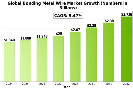
Global Bonding Metal Wire Market size was valued at US$ 1.84 billion in 2024 and is projected to reach US$ 2.73 billion by 2032, at a CAGR of 5.47% during the forecast period 2025-2032.
Bonding metal wires are ultra-thin metallic filaments used to create electrical interconnections in semiconductor packaging. These wires primarily consist of gold, aluminum, or copper materials and serve as conductive pathways between integrated circuit chips and their packaging substrates. The three dominant wire types include gold bonding wires (offering superior conductivity but higher cost), copper bonding wires (cost-effective with good thermal properties), and aluminum bonding wires (lightweight with excellent oxidation resistance).
The market growth is primarily driven by expanding semiconductor production, particularly in Asia-Pacific regions where countries like China, South Korea, and Taiwan dominate chip manufacturing. However, copper wire adoption faces challenges due to oxidation risks and specialized equipment requirements. Recent advancements include palladium-coated copper wires gaining traction for improved reliability. Key players like Heraeus and Tanaka are investing in R&D to develop advanced alloys that balance performance and cost-efficiency in response to evolving packaging technologies.
Get Full Report with trend analysis, growth forecasts, and Future strategies : https://semiconductorinsight.com/report/global-bonding-metal-wire-market/
Segment Analysis:
By Type
Copper Bonding Wires Dominate Due to Superior Electrical Conductivity and Cost Efficiency
The market is segmented based on type into:
Aluminum Bonding Wires
Subtypes: Ultra-thin aluminum wires, standard aluminum bonding wires
Copper Bonding Wires
Subtypes: Bare copper wires, coated copper wires
Gold Bonding Wires
Silver Bonding Wires
Others
By Application
Semiconductor Packaging Leads Demand Owing to Expanding Electronics Manufacturing
The market is segmented based on application into:
Semiconductor Packaging
PCB Assembly
Solar Panel Manufacturing
LED Packaging
Others
By Wire Diameter
Fine-Diameter Wires Hold Significant Share for Precision Interconnection Needs
The market is segmented based on wire diameter into:
Ultra-fine (<25μm)
Fine (25-50μm)
Standard (50-100μm)
Thick (>100μm)
By Bonding Method
Thermosonic Bonding Gains Preference for Reliable Interconnections in Advanced Packages
The market is segmented based on bonding method into:
Thermocompression Bonding
Thermosonic Bonding
Ultrasonic Bonding
Others
Regional Analysis: Metal Wire Market
North America North America represents a mature yet innovation-driven market for bonding metal wires, primarily fueled by the semiconductor and advanced electronics sectors. The U.S. accounts for approximately 38% of regional demand, supported by substantial R&D investments in semiconductor packaging technologies. Copper bonding wires are gaining traction due to their cost advantages over gold, though gold remains prevalent in high-reliability applications like aerospace and medical devices. Regulatory pressures related to material safety drive the adoption of eco-friendly alternatives, while the reshoring of electronics manufacturing under initiatives like the CHIPS Act presents growth opportunities. However, high labor costs and competitive pricing from Asian suppliers restrain market expansion.
Europe Europe’s market is characterized by stringent EU regulations on materials (e.g., RoHS directives) and a strong emphasis on precision engineering. Germany and the UK lead in demand, driven by automotive electronics and industrial automation sectors. The region is transitioning toward copper and palladium-coated wires to reduce dependency on gold, aligning with sustainability goals. While technological expertise remains high, slower growth in semiconductor production compared to Asia-Pacific limits volume expansion. Collaborative research between wire manufacturers and academic institutions, particularly in wafer-level packaging, is fostering niche innovations.
Asia-Pacific Dominating over 60% of global consumption, Asia-Pacific thrives due to concentrated semiconductor fabrication hubs in Taiwan, South Korea, and China. China’s aggressive investments in domestic chip production (e.g., $150 billion allocated under the “Made in China 2025” initiative) propel demand for cost-effective aluminum and copper wires. India and Southeast Asia are emerging hotspots, with PCB and consumer electronics manufacturing shifting to these regions. Price sensitivity favors local suppliers like MK Electron, though quality inconsistencies in low-tier products persist. The region’s rapid adoption of 5G and IoT devices further expands application scope.
South America The market remains nascent, with Brazil serving as the primary demand center for bonding wires used in automotive and consumer electronics assembly. Limited local semiconductor production restricts growth, with most wires imported from Asia or North America. Economic instability and currency fluctuations deter large-scale investments, though Mexico’s proximity to the U.S. supply chains offers modest opportunities. Copper wire adoption is slowly rising due to cost benefits, but gold retains dominance in legacy systems. Infrastructure gaps in technical training and testing facilities hinder market maturation.
Middle East & Africa This region exhibits the lowest market share but shows potential in semiconductor packaging for oil/gas sensors and telecommunications infrastructure. The UAE and Saudi Arabia lead with FDI-driven industrial diversification plans, while South Africa’s automotive sector utilizes bonding wires for electronic components. Dependence on imports and lack of localized R&D cap growth. However, partnerships with Asian wire manufacturers to establish distribution hubs could gradually improve accessibility. The focus remains on basic applications, with premium materials like gold used sparingly in niche segments.
MARKET OPPORTUNITIES
Automotive Electronics Expansion Opens New Growth Avenues
The automotive semiconductor market’s projected annual growth rate of 12% through 2030 presents significant opportunities for bonding wire manufacturers. Advanced driver assistance systems (ADAS) and vehicle electrification require specialized bonding solutions capable of withstanding harsh operating conditions. Manufacturers developing alloy wires with enhanced thermal and mechanical properties are capturing this high-margin segment, with some reporting 30% higher ASPs compared to standard bonding wires.
Emerging Markets Drive Infrastructure Investments
Southeast Asia’s semiconductor packaging industry is expanding rapidly, with new facility investments growing by 25% annually. This geographic shift in production is prompting bonding wire manufacturers to establish local operations, reducing logistics costs and improving customer responsiveness. Several leading producers have announced capacity expansions in Malaysia, Vietnam, and Thailand, with projected output increases of 40-50% over the next five years to serve these growing regional markets.
Advanced Material Innovations Create Premium Segments
Development of novel bonding wire alloys combining gold, palladium, and copper is enabling performance improvements in critical applications. These premium products command 50-70% price premiums over standard wires and are gaining traction in medical devices and aerospace electronics. Material science breakthroughs in wire surface treatments and dopants are further enhancing reliability, opening doors to applications requiring ultra-long product lifespans under extreme conditions.
GLOBAL BONDING METAL WIRE MARKET TRENDS
Shift Towards Copper Bonding Wires Accelerating Market Growth
The global bonding metal wire market is experiencing a pivotal shift from traditional gold bonding wires to copper-based alternatives, driven by cost efficiency and comparable performance characteristics. Copper bonding wires now account for approximately 38% of global semiconductor packaging applications, with projections indicating this share could exceed 45% by 2026. This transition is fueled by copper’s superior electrical conductivity (about 30% higher than gold) and significant cost savings—copper prices hover around $8,000 per metric ton compared to gold’s $60,000 per kilogram. Leading semiconductor manufacturers are adopting copper wires for power devices and memory packaging where thermal performance outweighs oxidation concerns.
Other Trends
Miniaturization in Semiconductor Packaging
The relentless drive towards smaller, more powerful electronics is pushing bonding wire technology to its physical limits. Ultra-fine bonding wires below 15μm diameter now represent over 28% of advanced packaging demand, particularly for high-density interconnect applications in 5G chips and IoT devices. This trend coincides with decreasing wire pitch requirements—from 60μm in 2018 to below 40μm in current designs—challenging manufacturers to improve break strength and looping consistency. The market for fine-pitch bonding wires is growing at a compound annual rate of 7.2%, outpacing conventional bonding wire segments.
Automotive Electronics Driving Specialty Alloy Development
Rising automotive electronics content—projected to reach $600 per vehicle by 2025—is creating demand for specialized bonding wires that withstand extreme temperatures and vibrational stress. Palladium-coated copper alloys now dominate this segment, offering 40% better high-temperature reliability than standard copper wires. The automotive bonding wire market segment expanded by 12% annually over the past three years, with electric vehicle power modules requiring up to 30% more bonding wire per unit than conventional automotive electronics. These harsh-environment applications are pushing manufacturers to develop novel alloy compositions with enhanced fatigue resistance.
COMPETITIVE LANDSCAPE
Key Industry Players
Market Dominated by Specialized Players with Strong Technological Capabilities
The global bonding metal wire market features a moderately concentrated competitive landscape, with leading companies holding significant market share through technological expertise and extensive distribution networks. Heraeus, the German multinational, leads the market with its advanced gold and aluminum bonding wire solutions, commanding approximately 18% of the global market share as of 2023. Their dominance stems from continuous R&D investments and strategic partnerships with semiconductor manufacturers.
Tanaka Holdings and Sumitomo Metal Mining represent strong Asian competitors, collectively holding over 25% market share. These Japanese firms benefit from proximity to major semiconductor fabrication plants in East Asia and have been expanding their copper bonding wire portfolios to meet growing demand for cost-effective alternatives to gold wires.
Meanwhile, mid-sized players like MK Electron and AMETEK are gaining traction through specialized product offerings. MK Electron’s ultra-fine diameter wires (15-50μm) have become particularly popular for advanced packaging applications, while AMETEK’s high-purity aluminum wires are seeing increased adoption in power semiconductor devices.
List of Key Metal Wire Companies Profiled
Heraeus (Germany)
Tanaka Holdings (Japan)
Sumitomo Metal Mining (Japan)
MK Electron (South Korea)
AMETEK (U.S.)
Doublink Solders (U.S.)
Yantai Zhaojin Kanfort (China)
Tatsuta Electric Wire & Cable (Japan)
Kangqiang Electronics (China)
The Prince & Izant (U.S.)
Learn more about Competitive Analysis, and Global Forecast of Global Bonding Metal Wire Market: https://semiconductorinsight.com/download-sample-report/?product_id=95877
FREQUENTLY ASKED QUESTIONS:
What is the current market size of Global Bonding Metal Wire Market?
-> Bonding Metal Wire Market size was valued at US$ 1.84 billion in 2024 and is projected to reach US$ 2.73 billion by 2032, at a CAGR of 5.47% during the forecast period 2025-2032.
Which key companies operate in Global Bonding Metal Wire Market?
-> Key players include Heraeus, Tanaka, Sumitomo Metal Mining, MK Electron, AMETEK, Doublink Solders, and Yantai Zhaojin Kanfort.
What are the key growth drivers?
-> Key growth drivers include rising semiconductor demand, miniaturization of electronics, and increasing adoption of advanced packaging technologies.
Which region dominates the market?
-> Asia-Pacific dominates the market with over 65% share, driven by semiconductor manufacturing hubs in China, Taiwan, South Korea, and Japan.
What are the emerging trends?
-> Emerging trends include copper wire adoption, fine-pitch bonding, and development of high-reliability alloys for automotive and industrial applications.
CONTACT US:
City vista, 203A, Fountain Road, Ashoka Nagar, Kharadi, Pune, Maharashtra 411014 +91 8087992013 [email protected]
Follow us on LinkedIn: https://www.linkedin.com/company/semiconductor-insight/
0 notes
Text
Trusted Copper Sheets Manufacturers in India – High-Performance Solutions by KWM India
Copper, with its unmatched electrical conductivity, thermal performance, and corrosion resistance, remains one of the most essential metals in various industries. Among the many copper products available in the market, copper sheets are highly sought-after due to their versatility, workability, and reliability in demanding applications. When it comes to top-quality copper sheets manufacturers in India, KWM India stands tall as a leading name, delivering precision-crafted copper sheets designed to meet both industrial and commercial requirements.
What Are Copper Sheets?
Copper sheets are flat-rolled products of copper, typically available in a wide range of thicknesses, lengths, and tempers. These sheets are widely used in applications that demand high electrical or thermal conductivity, corrosion resistance, and formability. From electrical panel manufacturing to architectural installations and from industrial heat exchangers to decorative metalwork, copper sheets serve a broad spectrum of uses.
The unique properties of copper—such as its antimicrobial nature, high recyclability, and resistance to atmospheric corrosion—make it an excellent material for both functional and aesthetic applications.
KWM India – Your Trusted Copper Sheet Manufacturer
As one of the most experienced and reputed copper sheet manufacturers in India, KWM India has been serving clients across industries with world-class non-ferrous metal solutions. With a strong legacy of quality, innovation, and customer focus, KWM has become a preferred supplier for copper products not only across India but also in international markets.
At KWM India, copper sheets are produced using high-grade raw materials and advanced rolling and finishing processes, ensuring accuracy, consistency, and reliability in every product.
Key Features of Copper Sheets by KWM India:
High Conductivity & Purity: KWM uses premium-grade electrolytic copper that ensures maximum conductivity, making it ideal for electrical and electronic applications.
Variety of Tempers & Thicknesses: Sheets are available in soft, half-hard, and hard tempers, with a wide range of thicknesses and sizes customized as per client needs.
Excellent Surface Finish: Copper sheets from KWM India offer a smooth, bright surface, making them suitable for decorative and architectural applications.
Corrosion & Oxidation Resistance: KWM ensures superior performance in harsh environments, making the sheets ideal for plumbing, roofing, marine, and industrial applications.
Precision Manufacturing: The company employs high-precision rolling mills and automated finishing systems to maintain tight tolerances and high dimensional accuracy.
Global Quality Standards: Every batch is manufactured under strict quality protocols, complying with national and international standards like ASTM, IS, and RoHS.
Applications of Copper Sheets
Thanks to their unique physical and chemical properties, copper sheets are used in a variety of sectors, such as:
Electrical & Electronics: Used for busbars, terminals, switchgear, PCB substrates, and connectors.
Architecture & Interior Design: Ideal for roofing, cladding, wall panels, backsplashes, and decorative metal elements.
Industrial Equipment: Utilized in heat exchangers, condensers, and chemical processing equipment for their excellent thermal transfer and corrosion resistance.
Automotive & Aerospace: Used in radiators, gaskets, and EMI shielding components.
Renewable Energy: Applied in solar panels, inverters, and battery connections due to their conductivity and durability.
Why Choose KWM India?
Experience & Expertise: With decades of expertise in the non-ferrous metals industry, KWM understands the unique needs of each sector.
Customized Solutions: From standard to highly customized sheet sizes and tempers, KWM delivers products tailored to specific requirements.
Advanced Infrastructure: Equipped with state-of-the-art machinery, testing labs, and logistics systems, KWM ensures consistency and timely delivery.
Sustainability Commitment: KWM follows eco-friendly manufacturing practices, minimizing waste and maximizing the use of recyclable materials.
Global Reach with Local Support: KWM serves clients across India and exports copper sheets to international markets with the same reliability and attention to detail.
Conclusion
If you are looking for reliable, high-quality copper sheets manufacturers in India, KWM India is the name to trust. With a legacy built on quality, technology, and customer satisfaction, KWM delivers copper sheets that meet the highest standards of performance and reliability.
Get in touch with KWM India today to explore their full range of copper sheet products or request a customized quote for your project needs.
Visit:- https://www.kmwindia.com/copper-sheets.html
0 notes
Text
Global Electronic Materials and Chemicals Market: Key Drivers, Challenges, and Opportunities
Growing Semiconductor and Electronics Manufacturing Drives Expansion in the Electronic Materials and Chemicals Market.
Electronic Materials and Chemicals Market Size was valued at USD 64.1 billion in 2023 and is expected to reach USD 110.2 billion by 2032 and grow at a CAGR of 6.2% over the forecast period 2024-2032.
The Electronic Materials and Chemicals Market is driven by the increasing demand for advanced electronic devices, semiconductors, and integrated circuits. These specialized materials and chemicals are vital in the manufacturing and functioning of products like chips, printed circuit boards (PCBs), displays, and solar panels. With the global rise in consumer electronics, electric vehicles (EVs), 5G infrastructure, and renewable energy technologies, the market is set for long-term expansion. Applications span across wafer fabrication, cleaning, etching, doping, and polishing, making electronic chemicals critical to precision and performance in modern electronics manufacturing.
Key Players:
The major key players are BASF, Air Products & Chemicals Inc., Albemarle Corporation, Air Liquide Holdings Inc., Ashland Inc., Bayer Ag, Linde Group, Honeywell International Inc., Cabot Microelectronics Corporation, Dow Chemical Company, Monsanto Electronic Materials Co., Hitachi Chemical Company, Brewer Science, Sumitomo Chemical, Shin-Etsu, Covestro, AZ Electronic Materials Plc, HD Microsystems, Drex-Chem Technologies, and other key players are mentioned in the final report.
Future Scope & Emerging Trends:
The future of the Electronic Materials and Chemicals Market is tightly linked to the growth of the semiconductor, EV, AI, and 5G sectors. With the miniaturization of devices and increasing complexity of chip designs, there is a rising need for high-purity, next-generation materials such as advanced photoresists, dielectric materials, and CMP slurries. The global semiconductor shortage has intensified investments in chip fabrication, particularly in the U.S., South Korea, Japan, and Taiwan, further boosting demand. Additionally, green manufacturing practices and environmentally friendly electronic chemicals are gaining traction as companies focus on reducing carbon footprints and adhering to stricter environmental regulations. Growth in quantum computing, IoT, and edge computing is also expected to open new frontiers in material innovation.
Key Points:
Critical for semiconductors, PCBs, displays, and solar cells.
Strong demand driven by consumer electronics, EVs, and 5G tech.
Increased R&D in high-purity, advanced chemical solutions.
Semiconductor manufacturing and chip fabrication are key growth drivers.
Sustainable and eco-friendly formulations gaining importance.
Asia-Pacific remains the largest and fastest-growing regional market.
Conclusion:
The Electronic Materials and Chemicals Market stands at the core of technological advancement, underpinning the performance and innovation of tomorrow’s electronic devices. With surging demand from semiconductor fabs, consumer tech, and renewable energy sectors, the market is poised for significant expansion. Industry leaders investing in cutting-edge materials, sustainability, and global supply chain resilience will play a crucial role in shaping the next era of electronic innovation.
Read Full Report: https://www.snsinsider.com/reports/electronic-materials-and-chemicals-market-4156
Contact Us:
Jagney Dave — Vice President of Client Engagement
Phone: +1–315 636 4242 (US) | +44- 20 3290 5010 (UK)
#Electronic Materials and Chemicals Market#Electronic Materials and Chemicals Market Size#Electronic Materials and Chemicals Market Share#Electronic Materials and Chemicals Market Report#Electronic Materials and Chemicals Market Forecast
0 notes