
"Quick FPC, Rigid-flex PCB prototype and PCB Assembly"Web:https://fpcway.com//Mob:086-15779653975E-mail: [email protected]
Don't wanna be here? Send us removal request.
Statistics
We looked inside some of the posts by fpcway-fpc and here's what we found interesting.
Average Info
Notes Per Post
0
Likes Per Post
0
Reblog Per Post
0
Reply Per Post
0
Time Between Posts
1 month
Number of Posts By Type
Text
4
Last Seen Tumblr Blogs


Fun Fact
The KCSC sent more than 20K requests to delete posts related to prostitution and porn to Tumblr from January to June 2017.
Text
Future Trends of Flexible Circuit Boards
Flexible circuit boards (flex PCBs) are continually evolving to meet the demands of various industries, including aerospace, medical, telecommunications, and consumer electronics. The future trends of flex PCBs are focused on advancing their capabilities in areas such as performance, miniaturization, and complexity.

One of the future trends of flex PCBs is increasing their performance capabilities. Future designs will incorporate more efficient and high-speed circuits, enabling faster data transfer rates, higher signal frequencies, and greater reliability. Additionally, enhanced materials such as high-thermal-conductivity laminates and stretchable conductive inks will improve heat management and mechanical stability in severe environments.
Another trend is the miniaturization of flex PCBs with improved geometries and finer trace widths. As portable devices trend towards smaller and more compact designs, flex PCBs offer the perfect solution by fitting into tight spaces, allowing for slim and sleek devices. Furthermore, advancements in flexible substrates, conductive adhesives, and interconnect technologies will enable even higher levels of miniaturization.
Complexity is another significant trend in the future of flex PCBs. The growing demand for advanced electronic devices requires greater functionalities, including complex interconnections, 3D structures, and multi-layered designs. Future flex PCB designs will incorporate innovative techniques such as laser drilling, sequential lamination, and embedded components, allowing for complex and intricate designs.
In conclusion, the future of flex PCBs is bright and promising, with vast opportunities for innovation and growth. At [company name], we are committed to providing cutting-edge solutions for our clients, keeping up with the latest trends and technologies in the industry. Contact us today to know more about our flexible circuit board services.

0 notes
Text
FPCway: Specialized manufacturer of flexible printed circuit boards
and rigid-flexible printed circuits
In today's fast-paced technology landscape, the demand for smaller, lighter, and more complex electronic devices continues to rise. Whether it's a sleek smartphone in your pocket or a sophisticated medical device in a hospital, these devices rely on cutting-edge printed circuit boards (PCBS) to run efficiently. Among the many types of printed circuit boards available, flexible printed circuits (flex PCBs) and rigid-flex printed circuits (Rigid-Flex PCBS) are increasingly favored due to their versatility and rich and diverse design possibilities.
Advantages of Flexible Printed Circuit (Flex PCB) :
Space efficiency: Very thin and lightweight, ideal for small electronic devices.
High reliability: Fewer interconnections and solder joints increase reliability and reduce points of failure.
Strong durability: Flexible printed circuits can withstand vibration, shock and extreme temperatures, making them ideal for harsh environments.
Freedom of design: The flexibility of the substrate allows for creative and innovative designs that may not be possible with rigid printed circuits.
Advantages of rigid-flex PCBs:
Space optimization: Flexible printed circuit (Flex PCB) components allow the integration of multiple PCBS and connectors, saving valuable space.
High reliability: Fewer connectors and solder joints reduce the risk of connection failure and signal loss.
Complex geometry: Rigid-flexible printed circuits can be designed to fit non-standard and irregular shaped enclosures.
Reduce weight: Reduce connectors and cables to reduce the overall weight of the device.
FPCway is a PCB manufacturing company located in Shenzhen, China, specializing in the manufacture of flexible printed circuit boards and rigid-flexible printed circuits. The circuit boards produced have been widely used in mobile communication, Internet of Things, optoelectronics, industrial control, medical equipment, consumer electronics and other high-tech industries. The products produced by FPCway are exported to all over the world. At present, FPCway has more than 5000 square meters of FPC workshop, which has 12 SMT production lines and 2 THT production lines. FPCway has more than 200 employees, with more than 20 senior executives with decades of industry experience. With this experience and advanced equipment, we have maintained excellent technical capabilities and strong competitiveness in the Flex PCB industry.
FPCway: From prototype to assembly to product
FPCway provides Flex PCB and rigid-flex PCBs from prototype design to assembly to product, while more than 200 professionals ensure zero defects and the fastest delivery time. The company sources materials from well-known brands and maintains ISO 9001, IATF16949 quality systems and UL certification, facilitating customers' access to commercial products.
Flexible PCB prototype: The production process of FPCB products usually starts from making prototypes, FPCWay almost does not limit the appearance size of FPCB, and can adjust the substrate, thickness and layer number of products according to customer needs.
Flexible PCB assembly: Bring goodness to life
Designing and manufacturing flexible printed circuits (flex PCBs) and rigid-flex PCBS is a highly specialized process that requires specialized knowledge and advanced equipment. Flexible printed circuit (Flex PCB) components are a key step in translating these innovative designs into functional electronic devices. FPCway's engineers consider the flexibility and form factor required by the customer to create a suitable flexible printed circuit (Flex PCB) layout choice; Secondly, the appropriate substrate material is selected based on factors such as flexibility, temperature resistance and intended application. The manufacturer then uses a combination of addition and subtraction processes to create the flexible circuit, which involves etching, drilling, and laminating together. FPCway uses advanced automatic pickers to precisely place components on manufacturing flexible printed circuits (flex PCBs) or rigid-flex PCBS, then apply solder paste to the component pads, heat the components to melt the solder and establish electrical connections. Finally, engineers ensure that flexible printed circuit (Flex PCB) or rigid-flex PCBs components meet quality and functional standards through rigorous testing to ensure that the product has zero defects.
FPCway through the construction of a strong talent team and increase capital investment in the purchase of new equipment, and from prototype design to assembly to the entire process of product accurate control, to ensure product quality, FPCway at a very competitive price to provide first-class service. The company stands out in the flexible printed circuit board industry for its superior technical capabilities, excellent product quality and timely delivery of products.
0 notes
Text
Special attention points for flexible circuit wiring
Layer stacking design, device layout, and cutting issues are all obvious, but there are many material weaknesses that can be encountered in flexible circuits.
From relatively high z-axis expansion coefficient adhesives to low viscosity PI substrate copper clad, to copper hardening and fatigue. The following statements of what to do and what not to do will focus on supplementing:
Maintaining the flexibility of the flexible board
It is obvious that the flexibility of the flexible circuit should be determined according to the needs in advance, but it still needs to be emphasized again. If the flexible circuit section is only intended to be folded during assembly and then installed in a fixed position, such as in a handheld ultrasound device, then we have a lot of freedom in choosing the number of layers and the type of copper skin (RA or ED). On the other hand, if the flexible circuit section is to be constantly moved, bent, or rotated, then the number of layers should be reduced and adhesive-free materials should be selected.
We can use IPC-2223B formulas (Formula 1 represents single-sided, Formula 2 represents double-sided, etc.) to determine the minimum allowable bending radius based on the allowable deformation of copper and other material properties.

This example formula is for a single-sided flexible board.
We choose EB based on actual usage conditions, with 16% for applications with little bending, 10% for flexible mounting applications, and 0.3% for dynamic flexible designs.
Do not bend at corners
Generally, we recommend keeping the copper trace of the flexible circuit bent along the vertical direction. But sometimes it's not possible, so try to minimize the bending amplitude and frequency, or use tapered bending according to mechanical design requirements.

Figure 1: Preferred bending location
Use arc routing
As shown in Figure 1 above, it is best to avoid using abrupt right angles or rigidly straight 45° angle traces, but rather to use an arc angle routing pattern. This can reduce the stress on the copper during bending.
Do not suddenly change the width of the trace
When the trace is connected to the pad, especially when arranging and arranging the flexible circuit terminals (as shown in the figure below), a weak force point will be formed, and the copper skin will easily age over time. Unless a reinforcing plate is used or the application process will not bend, it is recommended to use a gradually narrowing connection method such as the one shown below.

Figure 2: Sudden changes in trace width or connections to pads can create weak focal points
Use polygons
it is necessary to place a power supply or ground plane on a flexible board. If you don't mind significantly reducing flexibility and potentially causing the copper skin to wrinkle, you can choose to use solid copper. Generally speaking, it is best to use shadow polygon copper plating to maintain a high degree of flexibility. In mentioning this, I also think that traditional shadow polygons will have excess copper reinforcement in the directions of 0°, 90°, and 45°. A more optimized pattern is the hexagonal approach. This problem can be solved by using negative layer and arrayed hexagonal pads, and the shadow polygon can be established more quickly using copy and paste methods.

Figure 3: Using hexagonal copper plating can evenly balance the stress in three angles.
Provide reinforcement for pads
Due to the use of low-viscosity adhesives (relative to FR-4), copper on flexible circuits is more likely to detach from the polyimide substrate. Therefore, providing reinforcement for exposed copper is particularly important. Coated through holes provide appropriate anchoring for two flexible layers, so using vias is a very good reinforcement method. Because of this (providing z-axis expansion), many processing plants recommend adding coated through holes with depths up to 1.5 mils to rigid-flex boards and flexible circuits. Surface mount pads and non-coated through hole pads do not have reinforcement measures themselves, so additional reinforcement is needed to prevent detachment.

Figure 4: Reinforcement methods for flexible circuit pads, plating, increasing anchors, and reducing cover film openings
Referring to Figure 4, the second option is suitable for adhesive-type cover layers, and the third option is suitable for non-adhesive-type cover layers. Protective films using adhesives may exhibit "overflow" phenomena, so the gap between the pad and the opening must be large enough to ensure excellent soldering formation.
SMT component pads are the most fragile, especially when flexible circuits bend under the rigid pins and pads of the component. Figures 5 and 6 show how to reinforce the pads on both ends of the pad using a cover layer. To achieve this, the pads on the flexible board must be larger than the pads on a typical rigid board.
Looking at the comparison in Figure 6, SMD pads for installing components on a flexible board. This significantly reduces the installation density of flexible circuit components, but compared to rigid circuits, the density of flexible circuits cannot be too high in the first place.

Figure 5: SOW package cover film opening, showing its reinforcement on both ends of each pad. Figure 6: Adjusting pad size and cover layer openings

Figure 6: Adjusting pad size and cover layer openings.
Maintain double-sided flexibility
For dynamic double-sided flexible circuits, try to avoid placing traces in the same direction, but instead need to stagger them (Figure 7) to evenly distribute the copper trace (Figure 8).

Figure 7: Not recommended adjacent layer copper trace routing.

Figure 8: Preferred staggered adjacent layer copper trace routing.
0 notes
Text
What is FPC (Flexible Printed Circuit)?
1 Overview
FPC, also known as flexible printed circuit, is favored due to its lightweight, thin thickness, free bending and folding, and other excellent characteristics. With the rapid development of the electronics industry, circuit board design is increasingly moving towards high precision and high density. Traditional manual inspection methods can no longer meet production needs, and automatic defect detection of FPC has become an inevitable trend in industrial development.

Flexible printed circuit (FPC) is a technology developed by the United States in the 1970s to develop aerospace rocket technology. It is made of polyester film or polyimide as a substrate, with high reliability and good flexibility. By embedding circuit designs on flexible thin plastic sheets, a large number of precision components can be stacked in narrow and limited spaces to form flexible circuits. This circuit can be bent and folded at will, with light weight, small volume, good heat dissipation, and convenient installation, breaking through traditional interconnection technologies. In the structure of flexible circuits, materials include insulating films, conductors, and adhesives. Flexible printed circuits are the only solution that meets the requirements of miniaturization and mobility of electronic products. Flexible printed circuits can greatly reduce the volume and weight of electronic products, making them suitable for the development of electronic products towards high density, miniaturization, and high reliability.
2 FPC Composite Materials
Insulation Film:
Insulation films form the base layer of the circuit, and adhesives bond the copper foil to the insulation layer. In multi-layer designs, it is bonded to the inner layers. They are also used as protective covers to protect the circuit from dust and moisture and reduce stress during bending. Copper foil forms the conductive layer.
In some flexible circuits, the use of rigid elements made of aluminum or stainless steel can provide dimensional stability, provide physical support for the placement of components and wires, and eliminate stress. Adhesives bond the rigid elements and flexible circuits together. In addition, another material sometimes used in flexible circuits is the bonding layer, which is formed by applying adhesive to both sides of the insulation film. The bonding layer provides environmentally friendly and electrical insulation functions and can eliminate one layer of film, with the ability to bond multiple layers with a small amount of layers.
There are many types of insulation film materials, but the most commonly used are polyimide and polyester materials. Nearly 80% of all flexible circuit manufacturers in the United States use polyimide film materials, and about 20% use polyester film materials. Polyimide materials are non-flammable, geometrically stable, have high tear strength, and withstand welding temperatures. Polyester, also known as polyethylene terephthalate (PET), has physical properties similar to those of polyimide, has a lower dielectric constant, absorbs less moisture, but is not resistant to high temperatures. The melting point of polyester is 250°C, and the glass transition temperature (Tg) is 80°C, which limits their use in applications that require a large number of terminal welds. In low-temperature applications, they exhibit stiffness. However, they are suitable for mobile phones and other products that do not need to be exposed to harsh environments. Polyimide insulation films are usually combined with polyimide or acrylic adhesives, and polyester insulation materials are generally combined with polyester adhesives.
Conductors:
Copper foil is suitable for use in flexible circuits. It can be electroplated (ED) or electroplated. One side of the electroplated copper foil has a glossy surface, while the other side of the processed surface is dull. It is a flexible material that can be made in many thicknesses and widths. The matte surface of ED copper foil is often specially treated to improve its adhesion capacity. Forged copper foil, in addition to being flexible, also has the characteristics of rigidity and smoothness. Suitable for applications requiring dynamic deflection.
Adhesives:
Adhesives not only bond the insulation film to the conductive material but can also serve as a cover layer, as a protective coating, and as a cover coating. The main difference between the two lies in the application method used. The cover layer bonds with the cover insulation film to form a circuit with a laminated structure. Screen printing technology is used for the coverage and coating of adhesives. Not all laminate structures contain adhesives, and laminate structures without adhesives form thinner circuits and greater flexibility. Compared to adhesive-based laminate structures, it has better thermal conductivity. Since the thin structure of the non-adhesive flexible circuit and the elimination of the thermal resistance of the adhesive improve thermal conductivity. It can be used in working environments where adhesive-based laminate structures cannot be used.
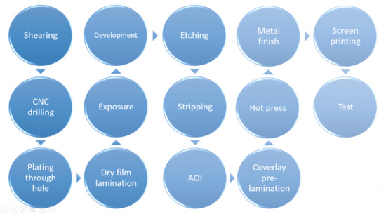
#3 FPC production process
#4 Advantages of Flexible Printed Circuits

Flexible printed circuit boards are printed circuits made of flexible insulating substrates, which have many advantages that rigid printed circuit boards do not have:
Flexible printed circuit boards Can bend freely, coil, fold, can be arranged according to any space layout requirements, and can move and expand in three-dimensional space.
The use of FPC can greatly reduce the volume and weight of electronic products, making them suitable for the development of electronic products towards high density, miniaturization, and high reliability. Therefore, FPC has been widely used in aerospace, military, mobile communication, notebook computers, computer peripherals, pdas, digital cameras and other fields or products.
FPC also has good heat dissipation and weldability, is easy to assemble, and has overall low cost advantages. The combination of soft and hard design also compensates to some extent for the slight lack of component carrying capacity of flexible substrates.
#5 FPC soldering operation steps
Before soldering, apply soldering flux to the pads and treat them with a soldering iron to prevent poor tin plating or oxidation of the pads from causing poor soldering. Chips generally do not require processing.
Use tweezers to carefully place the PQFP chip on the PCB board to avoid damaging the pins. Align it with the pad and ensure that the chip is placed in the correct direction. Adjust the temperature of the soldering iron to above 300 degrees Celsius, apply a small amount of solder to the tip of the soldering iron, press down the aligned chip with a tool, and add a small amount of solder to two diagonal pins. Hold the chip down and solder the pins at the two diagonal positions to secure the chip in place. After soldering the diagonals, recheck the alignment of the chip position. If necessary, adjust or remove and readjust the position on the PCB board.
When starting to solder all the pins, add solder to the tip of the soldering iron and apply soldering flux to all the pins to keep them moist. Touch the end of each pin of the chip with the tip of the soldering iron until you see the solder flowing into the pin. When soldering, the tip of the soldering iron should be parallel to the soldering pin to prevent overlapping due to excessive soldering.
After soldering all the pins, moisten all the pins with flux to clean the solder. Suck up any excess solder to eliminate any shorts or overlaps. Finally, use tweezers to check for misaligned soldering. After checking, remove the solder from the circuit board, soak a stiff brush in alcohol, and carefully wipe along the pin direction until the solder disappears.
SMD resistor-capacitor components are relatively easy to solder. You can first place it on the pad, then place one end of the component on it, use tweezers to hold the component, and then solder one end before checking if it is placed correctly. If it is already aligned, then solder the other end.
Click here for more information:https://fpcway.com/

0 notes