#16 bit special embedded microcontroller
Explore tagged Tumblr posts
Visit Tumblr Blog
Explore Tumblr blogs with no restrictions, modern design and the best experience.
Last Seen Tumblr Blogs


Fun Fact
The KCSC sent more than 20K requests to delete posts related to prostitution and porn to Tumblr from January to June 2017.
Text
https://www.futureelectronics.com/p/semiconductors--microcontrollers--16-bit-general-purpose/mc812a4cpve8-nxp-6048193
General purpose microcontrollers, lcd microcontroller, Pic microcontrollers
MC812A4 Series 1 kB RAM 16-Bit Low Power High Speed Microcontroller - LQFP-112
#Microcontrollers#16 bit General Purpose#MC812A4CPVE8#NXP#lcd microcontroller#Pic microcontrollers#What is a wireless microcontroller#16 bit special embedded microcontroller#16-Bit Low Power High Speed Microcontroller
1 note
·
View note
Text
https://www.futureelectronics.com/p/semiconductors--microcontrollers--16-bit-general-purpose/mchc912b32cfue8-nxp-3822756
Microprocessor development board, 16 bit special embedded microcontroller
MCHC91B Series 1 kB RAM 32 kB Flash 16-Bit SMT Flash Microcontroller - QFP-80
#Microcontrollers#16 bit General Purpose#MCHC912B32CFUE8#NXP#microprocessor development board#16 bit special embedded#wireless microcontroller#16 bit embedded#lcd#What is a 16-bit microchip#16-bit microchip inventor#Microcontrollers software
1 note
·
View note
Text
https://www.futureelectronics.com/p/semiconductors--analog--amplifiers--general-purpose/ts391iylt-stmicroelectronics-5071806
Amplifiers, 16 bit microcontroller, lcd microcontrollers, wireless microcontroller
TS391 Series 36 V 400 nA SMT Single General Purpose Comparator - SOT-23
#STMicroelectronics#TS391IYLT#Operational#General Purpose Amplifiers. Amplifiers#16 bit#lcd#wireless#embedded microcontroller manufacturers#embedded microcontrollers software#What is a lcd microcontroller#special programmable
1 note
·
View note
Text
The story linked by @hawkuletz tho:
The King's Toaster
The King's Toaster
Anonymous
Once upon a time, in a kingdom not far from here, a king summoned two of his advisors for a test. He showed them both a shiny metal box with two slots in the top, a control knob and a lever.
"What do you think this is?"
One advisor, an engineer, answered first. "It is a toaster," he said.
The king asked, "How would you design an embedded computer for it?"
The engineer replied, "Using a four-bit microcontroller, I would write a simple program that reads the darkness knob and quantizes its position to one of 16 shades of darkness, from snow white to coal black. The program would use that darkness level as the index to a 16-element table of initial timer values. Then it would turn on the heating elements and start the timer with the initial value selected from the table. At the end of the time delay, it would turn off the heat and pop up the toast. Come back next week, and I'll show you a working prototype."
The second advisor, a computer scientist, immediately recognized the danger of such short-sighted thinking. He said, "Toasters don't just turn bread into toast, they are also used to warm frozen waffles. What you see before you is really a breakfast food cooker. As the subjects of your kingdom become more sophisticated, they will demand more capabilities. They will need a breakfast food cooker that can also cook sausage, fry bacon, and make scrambled eggs. A toaster that only makes toast will soon be obsolete. If we don't look to the future, we will have to completely redesign the toaster in just a few years.
With this in mind, we can formulate a more intelligent solution to the problem. First, create a class of breakfast foods. Specialize this class into subclasses: grains, pork and poultry. The specialization process should be repeated with grains divided into toast, muffins, pancakes and waffles; pork divided into sausage, links and bacon; and poultry divided into scrambled eggs, hard-boiled eggs, poached eggs, fried eggs, and various omelet classes.
The ham and cheese omelet class is worth special attention because it must inherit characteristics from the pork, dairy and poultry classes. Thus, we see that the problem cannot be properly solved without multiple inheritance. At run time, the program must create the proper object and send a message to the object that says, 'Cook yourself'. The semantics of this message depend, of course, on the kind of object, so they have a different meaning to a piece of toast than to scrambled eggs.
Reviewing the process so far, we see that the analysis phase has revealed that the primary requirement is to cook any kind of breakfast food. In the design phase, we have discovered some derived requirements. Specifically, we need an object-oriented language with multiple inheritance. Of course, users don't want the eggs to get cold while the bacon is frying, so concurrent processing is required, too.
We must not forget the user interface. The lever that lowers the food lacks versatility and the darkness knob is confusing. Users won't buy the product unless it has a user-friendly, graphical interface.
When the breakfast cooker is plugged in, users should see a cowboy boot on the screen. Users click on it and the message 'Booting UNIX v. 8.3' appears on the screen. (UNIX 8.3 should be out by the time the product gets to the market.) Users can pull down a menu and click on the foods they want to cook.
Having made the wise decision of specifying the software first in the design phase, all that remains is to pick an adequate hardware platform for the implementation phase. An Intel 80386 with 8MB of memory, a 30MB hard disk and a VGA monitor should be sufficient. If you select a multitasking, object oriented language that supports multiple inheritance and has a built-in GUI, writing the program will be a snap. (Imagine the difficulty we would have had if we had foolishly allowed a hardware-first design strategy to lock us into a four-bit microcontroller!)."
The king had the computer scientist thrown in the moat, and they all lived happily ever after.
35K notes
·
View notes
Text
Basic Understanding of 8051 Microcontroller
8051 Microcontroller
Hello, and welcome to my blog! Today I’m going to talk about one of my favorite topics: the 8051 microcontroller. If you are interested in embedded systems, you might have heard of this amazing device that can do wonders with just a few pins and bytes of memory. But what exactly is a 8051 microcontroller, and how does it work? Let’s find out!
A 8051 microcontroller is a small computer that can be programmed to perform various tasks. It has a central processing unit (CPU) that executes instructions, a random access memory (RAM) that stores data, a read-only memory (ROM) that stores the program code, and input/output (I/O) ports that connect to external devices. The 8051 microcontroller belongs to the family of 8-bit microcontrollers, which means that each instruction and data is 8 bits long (one byte).
The 8051 microcontroller has some special features that make it suitable for embedded applications. For example, it has four register banks that can be switched quickly to optimize performance. It also has two 16-bit timers/counters that can be used for timing and counting events. It has a serial port that can communicate with other devices using serial communication protocols. It has five interrupt sources that can respond to external or internal events. And it has four I/O ports that can be configured as input or output pins.
One of the advantages of the 8051 microcontroller is that it is easy to program and debug. There are many development tools available for the 8051 microcontroller, such as compilers, assemblers, simulators, emulators, and programmers. You can write your code in assembly language or in a high-level language such as C or BASIC. You can test your code on a simulator or on a real device using an emulator or a programmer.
Another advantage of the 8051 microcontroller is that it is widely used and supported. There are many variants and derivatives of the 8051 microcontroller from different manufacturers, such as Intel, Atmel, Philips, and Microchip. You can find many resources and tutorials online to learn more about the 8051 microcontroller and its applications. You can also find many projects and examples that use the 8051 microcontroller for various purposes, such as robotics, home automation, security systems, and games.
If you are interested to understand more about the 8051 microcontroller, then you can go through the PiEmbSysTech 8051 microcontroller Tutorial Blog. If you have any questions or query, that you need to get answer or you have any idea to share it with the community, you can use Piest Forum.
I hope you enjoyed this blog post and learned something new about the 8051 microcontroller. If you have any questions or comments, please feel free to leave them below. And don’t forget to subscribe to my blog for more interesting posts about embedded systems.
Thanks for reading!
0 notes
Text
Microchip Technology Inc 2022 Hiring Freshers as Internship at Bengaluru, Karnataka
Microchip Technology Inc 2022 Hiring Freshers as Internship at Bengaluru, Karnataka | Job Title: Internship | Degree needed: BE, BTech | Pass-out Year: 2021, 2022 | Location: Bengaluru, Karnataka | Experience: Fresher
Microchip Technology Inc Recruitment Drive for 2022 Fresher Microchip Technology Inc 2022 Hiring Freshers as Internship at Bengaluru, Karnataka About the Company: Microchip Technology Inc. is a leading provider of embedded control applications. Our product portfolio comprises general purpose and specialized 8-bit, 16-bit, and 32-bit microcontrollers, 32-bit microprocessors, field-programmable…

View On WordPress
0 notes
Text
MicroChip Hiring Freshers For Software Engineer - I Position- BE/BTech/MCA
MicroChip Hiring Freshers For Software Engineer – I Position- BE/BTech/MCA
MicroChip Hiring Freshers For Software Engineer Details: Company Description: Microchip Technology Inc. is a leading provider of embedded control applications. Our product portfolio comprises general purpose and specialized 8-bit, 16-bit, and 32-bit microcontrollers, 32-bit microprocessors, field-programmable gate array (FPGA) products, a broad spectrum of high-performance linear, mixed-signal,…
View On WordPress
0 notes
Text
Microcontroller ATTINY44A
In almost every system existing today, an automatically controlled mechanism is preferred. From office to home they are used in every gadget to make our life less hectic, fast, and energy-efficient. Microprocessors and microcontrollers serve this purpose. ATTINY44A is a microcontroller with RAM, ROM, Input, and Output ports electronics supplies. Depending on the task, it is convenient to select the type of controller that fits well for the desired purpose. Generally, two parameters are kept in mind while selecting the controller's first power consumption and the other processing speed. Both are at the expense of one and another. ATTINY44A performs smartly between these parameters by executing powerful instructions in one clock because of its ability to optimize itself at the most efficient point. Furthermore, it has a variety of options and control capabilities. If one has extraordinary programming skills the ATTINY44A outperforms CISCs.

ATTINY44A is low power 8-bit, 14-pin PDIP/SOIC packaged AVR microcontroller, accredited to Microchip Technology Inc. famously known for microcontrollers and integrated circuits. With the invention of these modules, electronic tasks can be easily and readily achieved. Operating at a voltage range of 1.8V-5.5V. If the ATTINY44A is operating at 2.7 volts its speed grade ranges from 0 to 10MHz but if it is operating at less than the aforementioned volts its grading speed reduces from 0 to 4MHz.
Further details are thoroughly mentioned in the respective datasheet. It has Reduced Instruction Set Computer (RISC) architecture which gives a significant advantage of processing speed since Complex Instruction Set Computer (CISC) architecture is comparatively slow per instruction. Moreover, it upholds the advantage of using fewer transistors because it executes simple instructions and is thus relatively smaller in size. RISC-based architectures are easier to design and are available in a low purchasing range as compared to CISC-based microcontrollers. ATTINY44A has RISC architecture therefore it can be used for implementing multiple tasks. It executes powerful instructions of 120 in a clock cycle with full static operation. Furthermore, it has 32x8 general-purpose registers and a programmable watchdog timer.
Some other features are segments of non-volatile memory and high endurance. Its non-volatile memory segments include in-built flash memory of 4KB storage with 10,000 write and erase repetitions, in-built EEPROM of 256 bytes storage with 100,000 cycles, and in-built 256 bytes SRAM. It retains data according to the given temperature conditions. For example, it can keep data safe for 20 years at 85 degrees ⁰C and 100 years at 25 ⁰C. It has another great feature of locking self-programming characteristics concerned with EEPROM and flash memory to keep previous data secured. Its peripheral features incorporate 8-bit and 16-bit timer & counter, universal serial interface (USI), two PWM channels, ADC along with on-logic chip analog comparator and oscillator while its special features comprise of a debug system, SPI port, stand-by, and power-down modes, ADC noise reduction, an on- logic chip temperature sensor, reset circuit and brownout detection circuit along with software disable the function.
ATTINY44A is mainly used in automation industries for the production of abundant materials and goods in less time. It can be incorporated into various other fields such as robotics, aeronautics, and embedded systems. Its widely found application is in power management for careful monitoring and continuation of the system. It performs competently in silicon-organic hybrid voltage equalizer by protecting and balancing charging factors of super-capacitor for sale.
0 notes
Text
Optimizing a low-cost camera for machine vision
In this deep dive article, performance optimization specialist Larry Bank (a.k.a The Performance Whisperer) takes a look at the work he did for the Arduino team on the latest version of the Arduino_OV767x library.

Arduino recently announced an update to the Arduino_OV767x camera library that makes it possible to run machine vision using TensorFlow Lite Micro on your Arduino Nano 33 BLE board.
If you just want to try this and run machine learning on Arduino, you can skip to the project tutorial.
The rest of this article is going to look at some of the lower level optimization work that made this all possible. There are higher performance industrial-targeted options like the Arduino Portenta available for machine vision, but the Arduino Nano 33 BLE has sufficient performance with TensorFlow Lite Micro support ready in the Arduino IDE. Combined with an OV767x module makes a low-cost machine vision solution for lower frame-rate applications like the person detection example in TensorFlow Lite Micro.
Need for speed
Recent optimizations done by Google and Arm to the CMSIS-NN library also improved the TensorFlow Lite Micro inference speed by over 16x, and as a consequence bringing down inference time from 19 seconds to just 1.2 seconds on the Arduino Nano 33 BLE boards. By selecting the person_detection example in the Arduino_TensorFlowLite library, you are automatically including CMSIS-NN underneath and benefitting from these optimizations. The only difference you should see is that it runs a lot faster!
The CMSIS-NN library provides optimized neural network kernel implementations for all Arm’s Cortex-M processors, ranging from Cortex-M0 to Cortex-M55. The library utilizes the processor’s capabilities, such as DSP and M-Profile Vector (MVE) extensions, to enable the best possible performance.
The Arduino Nano 33 BLE board is powered by Arm Cortex-M4, which supports DSP extensions. That will enable the optimized kernels to perform multiple operations in one cycle using SIMD (Single Instruction Multiple Data) instructions. Another optimization technique used by the CMSIS-NN library is loop unrolling. These techniques combined will give us the following example where the SIMD instruction, SMLAD (Signed Multiply with Addition), is used together with loop unrolling to perform a matrix multiplication y=a*b, where
a=[1,2]
and
b=[3,5 4,6]
a, b are 8-bit values and y is a 32-bit value. With regular C, the code would look something like this:
for(i=0; i<2; ++i) for(j=0; j<2; ++j) y[i] += a[j] * b[j][i]
However, using loop unrolling and SIMD instructions, the loop will end up looking like this:
a_operand = a[0] | a[1] << 16 // put a[0], a[1] into one variable for(i=0; i<2; ++i) b_operand = b[0][i] | b[1][i] << 16 // vice versa for b y[i] = __SMLAD(a_operand, b_operand, y[i])
This code will save cycles due to
fewer for-loop checks
__SMLAD performs two multiply and accumulate in one cycle
This is a simplified example of how two of the CMSIS-NN optimization techniques are used.
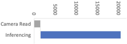
Figure 1: Performance with initial versions of libraries
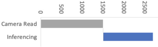
Figure 2: Performance with CMSIS-NN optimizations
This improvement means the image acquisition and preprocessing stages now have a proportionally bigger impact on machine vision performance. So in Arduino our objective was to improve the overall performance of machine vision inferencing on Arduino Nano BLE sense by optimizing the Arduino_OV767X library while maintaining the same library API, usability and stability.

Figure 3: Performance with CMSIS-NN and camera library optimizations
For this, we enlisted the help of Larry Bank who specializes in embedded software optimization. Larry’s work got the camera image read down from 1500ms to just 393ms for a QCIF (176×144 pixel) image. This was a great improvement!
Let’s have a look at how Larry approached the camera library optimization and how some of these techniques can apply to your Arduino code in general.
Performance optimizing Arduino code
It’s rarely practical or necessary to optimize every line of code you write. In fact there are very good reasons to prioritize readable, maintainable code. Being readable and optimized don’t necessarily have to be mutually exclusive. However, embedded systems have constrained resources, and when applications demand more performance, some trade-offs might have to be made. Sometimes it is necessary to restructure algorithms, pay attention to compiler behavior, or even analyze timing of machine code instructions in order to squeeze the most out of a microcontroller. In some cases this can make the code less readable — but the beauty of an Arduino library is that this can be abstracted (hidden) from user sketch code beneath the cleaner library function APIs.
What does “Camera.readFrame” do?
We’ve connected a camera to the Arduino. The Arduino_OV767X library sets up the camera and lets us transfer the raw image data from the camera into the Arduino Nano BLE memory. The smallest resolution setting, QCIF, is 176 x 144 pixels. Each pixel is encoded in 2 bytes. We therefore need to transfer at least 50688 bytes (176 x 144 x 2 ) every time we capture an image with Camera.readFrame. Because the function is performing a byte read operation over 50 thousand times per frame, the way it’s implemented has a big impact on performance. So let’s have a look at how we can most efficiently connect the camera to the Arduino and read a byte of data from it.
Philosophy
I tend to see the world of code through the “lens” of optimization. I’m not advocating for everyone to share my obsession with optimization. However, when it does become necessary, it’s helpful to understand details of the target hardware and CPU. What I often encounter with my clients is that their code implements their algorithm neatly and is very readable, but it’s not necessarily ‘performance friendly’ to the target machine. I assume this is because most people see code from a top-down approach: they think in terms of the abstract math and how to process the data. My history in working with very humble machines and later turning that into a career has flipped that narrative on its head. I see software from the bottom up: I think about how the memory, I/O and CPU registers interact to move and process the data used by the algorithm. It’s often possible to make dramatic improvements to the code execution speed without losing any of its readability. When your readable/maintainable solution still isn’t fast enough, the next phase is what I call ‘uglification.’ This involves writing code that takes advantage of specific features of the CPU and is nearly always more difficult to follow (at least at first glance!).
Optimization methodology
Optimization is an iterative process. I usually work in this order:
Test assumptions in the algorithm (sometimes requires tracing the data)
Make innocuous changes in the logic to better suit the CPU (e.g. change modulus to logical AND)
Flatten the hierarchy or simplify overly nested classes/structures
Test any slow/fast paths (aka statistics of the data — e.g. is 99% of the incoming data 0?)
Go back to the author(s) and challenge their decisions on data precision / storage
Make the code more suitable for the target architecture (e.g. 32 vs 64-bit CPU registers)
If necessary (and permitted by the client) use intrinsics or other CPU-specific features
Go back and test every assumption again
If you would like to investigate this topic further, I’ve written a more detailed presentation on Writing Performant C++ code.
Depending on the size of the project, sometimes it’s hard to know where to start if there are too many moving parts. If a profiler is available, it can help narrow the search for the “hot spots” or functions which are taking the majority of the time to do their work. If no profiler is available, then I’ll usually use a time function like micros() to read the current tick counter to measure execution speed in different parts of the code. Here is an example of measuring absolute execution time on Arduino:
long lTime; lTime = micros(); <do the work> iTime = micros() - lTime; Serial.printf(“Time to execute xxx = %d microseconds\n”, (int)lTime);
I’ve also used a profiler for my optimization work with OpenMV. I modified the embedded C code to run as a MacOS command line app to make use of the excellent XCode Instruments profiler. When doing that, it’s important to understand how differently code executes on a PC versus embedded — this is mostly due to the speed of the CPU compared to the speed of memory.
Pins, GPIO and PORTs
One of the most powerful features of the Arduino platform is that it presents a consistent API to the programmer for accessing hardware and software features that, in reality, can vary greatly across different target architectures. For example, the features found in common on most embedded devices like GPIO pins, I2C, SPI, FLASH, EEPROM, RAM, etc. have many diverse implementations and require very different code to initialize and access them.
Let’s look at the first in our list, GPIO (General Purpose Input/Output pins). On the original Arduino Uno (AVR MCU), the GPIO lines are arranged in groups of 8 bits per “PORT” (it’s an 8-bit CPU after all) and each port has a data direction register (determines if it’s configured for input or output), a read register and a write register. The newer Arduino boards are all built around various Arm Cortex-M microcontrollers. These MCUs have GPIO pins arranged into groups of 32-bits per “PORT” (hmm – it’s a 32-bit CPU, I wonder if that’s the reason). They have a similar set of control mechanisms, but add a twist — they include registers to SET or CLR specific bits without disturbing the other bits of the port (e.g. port->CLR = 1; will clear GPIO bit 0 of that port). From the programmer’s view, Arduino presents a consistent set of functions to access these pins on these diverse platforms (clickable links below to the function definitions on Arduino.cc):
pinMode(pin, mode); digitalRead(pin); digitalWrite(pin, value);
For me, this is the most powerful idea of Arduino. I can build and deploy my code to an AVR, a Cortex-M, ESP8266 or an ESP32 and not have to change a single line of code nor maintain multiple build scripts. In fact, in my daily work (both hobby and professional), I’m constantly testing my code on those 4 platforms. For example, my LCD/OLED display library (OneBitDisplay) can control various monochrome LCD and OLED displays and the same code runs on all Arduino boards and can even be built on Linux.
One downside to having these ‘wrapper’ functions hide the details of the underlying implementation is that performance can suffer. For most projects it’s not an issue, but when you need to get every ounce of speed out of your code, it can make a huge difference.
Camera data capture
One of the biggest challenges of this project was that the original OV7670 library was only able to run at less than 1 frame per second (FPS) when talking to the Nano 33. The reason for the low data rate is that the Nano 33 doesn’t expose any hardware which can directly capture the parallel image data, so it must be done ‘manually’ by testing the sync signals and reading the data bits through GPIO pins (e.g. digitalRead) using software loops. The Arduino pin functions (digitalRead, digitalWrite) actually contain a lot of code which checks that the pin number is valid, uses a lookup table to convert the pin number to the I/O port address and bit value and may even disable interrupts before reading or changing the pin state. If we were to use the digitalRead function for an application like this, it would limit the data capture rate to be too slow to operate the camera. You’ll see this further down when we examine the actual code used to capture the data.
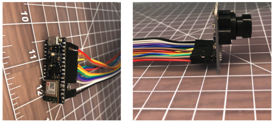
First, a quick review of the OV7670 camera module: According to its datasheet, it’s capable of capturing a VGA (640×480) color image at up to 30 FPS. The kit used for this project has the camera mounted to a small PCB and presents an 8-bit parallel data bus and various sync signals.

It requires an external “master clock” (MCLK in the photo) to drive its internal state machine which is used to generate all of the other timing signals. The Nano 33 can provide this external clock source by using its I2S clock. The OV767X library sets this master clock to 16Mhz (the camera can handle up to 48Mhz) and then there is a set of configuration registers to divide this value to arrive at the desired frame rate. Only a few possible frame rates are available (1, 5, 10, 15, 20, and 30 FPS).

Above is one of the timing diagrams from the OV7670 datasheet. This particular drawing shows the timing of the data for each byte received along each image row. The HREF signal is used to signal the start and end of a row and then each byte is clocked in with the PCLK signal. The original library code read each bit (D0-D7) in a loop and combined them together to form each data byte. The image data comes quickly, so we have very little time to read each byte. Assembling them one bit at a time is not very efficient. You might be thinking that it’s not that hard of a problem to solve on the Nano 33. After all, it has 22 GPIO pins and the Cortex-M inside it has 32-bit wide GPIO ports, so just hook up the data bits sequentially and you’ll be able to read the 8 data bits in one shot, then Mission Accomplished

. If only things were that easy. The Nano 33 does have plenty of GPIO pins, but there isn’t a continuous sequence of 8 bits available using any of the pins! I’m guessing that the original code did it one bit at a time because it didn’t look like there was a better alternative. In the pinout diagram below, please notice the P0.xx and P1.xx numbers. These are the Cortex-M GPIO port 0 and 1-bit numbers (other Cortex-M processors would label them PA and PB).
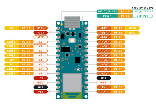
I wasn’t going to let this little bump in the road stop me from making use of bit parallelism. If you look carefully at the bit positions, the best continuous run we can get is 6 bits in a row with P1.10 through P1.15. It’s not possible to read the 8 data bits in one shot…or is it? If we connect D0/D1 of the camera to P1.02/P1.03 and D2-D7 to P1.10-P1.15, we can do a single 32-bit read from port P1 and get all 8 bits in one shot. The bits are in order, but will have a gap between D1 and D2 (P1.04 to P1.09). Luckily the Arm CPU has what’s called a barrel shifter. It also has a smart instruction set which allows data to be shifted ‘for free’ at the same time the instruction is doing something else. Let’s take a look at how and why I changed the code:
Original:
uint8_t in = 0; for (int k = 0; k < 8; k++) { bitWrite(in, k, (*_dataPorts[k] & _dataMasks[k]) != 0); }
Optimized:
uint32_t in = port->IN; // read all bits in parallel in >>= 2; // place bits 0 and 1 at the "bottom" of the register in &= 0x3f03; // isolate the 8 bits we care about in |= (in >> 6); // combine the upper 6 and lower 2 bits
Code analysis
If you’re not interested in the nitty gritty details of the code changes I made, you can skip this section and go right to the results below.First, let’s look at what the original code did. When I first looked at it, I didn’t recognize bitWrite; apparently it’s not a well known Arduino bit manipulation macro; it’s defined as:
#define bitWrite(value, bit, bitvalue) (bitvalue ? bitSet(value, bit) : bitClear(value, bit))
This macro was written with the intention of being used on GPIO ports (the variable value) where the logical state of bitvalue would be turned into a single write of a 0 or 1 to the appropriate bit. It makes less sense to be used on a regular variable because it inserts a branch to switch between the two possible outcomes. For the task at hand, it’s not necessary to use bitClear() on the in variable since it’s already initialized to 0 before the start of each byte loop. A better choice would be:
if (*_dataPorts[k] & _dataMasks[k]) in |= (1 << k);
The arrays _dataPorts[] and _dataMasks[] contain the memory mapped GPIO port addresses and bit masks to directly access the GPIO pins (bypassing digitalRead). So here’s a play-by-play of what the original code was doing:
Set in to 0
Set k to 0
Read the address of the GPIO port from _dataPorts[] at index k
Read the bit mask of the GPIO port from _dataMasks[] at index k
Read 32-bit data from the GPIO port address
Logical AND the data with the mask
Shift 1 left by k bits to prepare for bitClear and bitSet
Compare the result of the AND to zero
Branch to bitSet() code if true or use bitClear() if false
bitClear or bitSet depending on the result
Increment loop variable k
Compare k to the constant value 8
Branch if less back to step 3
Repeat steps 3 through 13, 8 times
Store the byte in the data array (not shown above)
The new code does the following:
Read the 32-bit data from the GPIO port address
Shift it right by 2 bits
Logical AND (mask) the 8 bits we’re interested in
Shift and OR the results to form 8 continuous bits
Store the byte in the data array (not shown above)
Each of the steps listed above basically translates into a single Arm instruction. If we assume that each instruction takes roughly the same amount of time to execute (mostly true on Cortex-M), then old vs. new is 91 versus 5 instructions to capture each byte of camera data, an 18x improvement! If we’re capturing a QVGA frame (320x240x2 = 153600 bytes), that becomes many millions of extra instructions.
Results
The optimized byte capture code translates into 5 Arm instructions and allows the capture loop to now handle a setting of 5 FPS instead of 1 FPS. The FPS numbers don’t seem to be exact, but the original capture time (QVGA @ 1 FPS) was 1.5 seconds while the new capture time when set to 5 FPS is 0.393 seconds. I tested 10 FPS, but readFrame() doesn’t read the data correctly at that speed. I don’t have an oscilloscope handy to probe the signals to see why it’s failing. The code may be fast enough now (I think it is), but the sync signals may become too unstable at that speed. I’ll leave this as an exercise to the readers who have the equipment to see what happens to the signals at 10 FPS.
For the work I did on the OV767X library, I created a test fixture to make sure that the camera data was being received correctly. For ML/data processing applications, it’s not necessary to do this. The built-in camera test pattern can be used to confirm the integrity of the data by using a CRC32.
My tinned protoboard test fixture with 320×240 LCD
Note: The frames come one immediately after another. If you capture a frame and then do some processing and then try to capture another frame, you may hit the middle of the next frame when you call readFrame(). The code will then wait until the next VSync signal, so that frame’s capture time could be as much as 2x as long as a single frame time.
More tips
I enjoy testing the limits of embedded hardware, especially when it involves bits, bytes and pixels. I’ve written a few blog posts that explore the topics of speed and power usage if you’re interested in learning more about it.
Conclusion
The embedded microcontrollers available today are capable of handling jobs that were unimaginable just a few years ago.
Optimized ML solutions from Google and Edge Impulse are capable of running on low-cost, battery-powered boards (vision, vibration, audio, whatever sensor you want to monitor).
Python and Arduino programming environments can test your project idea with little effort.
Software can be written an infinite number of ways to accomplish the same task, but one constant remains: TANSTATFC (there ain’t no such thing as the fastest code).
Never assume the performance you’re seeing is what you’re stuck with. Think of existing libraries and generic APIs available through open source libraries and environments as a starting point.
Knowing a bit of info about the target platform can be helpful, but it’s not necessary to read the MCU datasheet. In the code above, the larger concept of Arm Cortex-M 32-bit GPIO ports was sufficient to accomplish the task without knowing the specifics of the nRF52’s I/O hardware.
Don’t be afraid to dig a little deeper and test every assumption.
If you encounter difficulties, the community is large and there are a ton of resources out there. Asking for help is a sign of strength, not weakness.
Optimizing a low-cost camera for machine vision was originally published on PlanetArduino
0 notes
Text
Global Automotive Microcontrollers Market 2019-2023
The global automotive microcontrollers market is expected to post a CAGR close to 1% during the period 2019-2023, according to the latest market research report by Technavio.

A key factor driving the growth of the market is the increase in electronic content in vehicles owing to stringent regulations targeted at controlling emissions. The emission of harmful greenhouse gases has been increasing at an alarming rate in most countries. Therefore, regulatory standards pertaining to fuel efficiency have led to a surge in electronic content in modern vehicles. The basic objective of regulators is to reduce fuel consumption by increasing the efficiency of modern vehicles and through the adoption of an alternative medium, such as electricity. Hence, the focus on electrification will be more beneficial for automotive OEMs compared with spending considerably on compliance with stringent fuel economy standards, thereby driving market growth. Many governments worldwide have shifted their focus toward the adoption of cleaner technology. Battery- powered electric vehicles are more efficient and do not emit harmful gases as is the case with internal combustion engine powered vehicles. All these factors are expected to boost market growth over the forecast period.
As per Technavio, the development of new flash technology in automotive microcontrollers will have a positive impact on the market and contribute to its growth significantly over the forecast period. This global automotive microcontrollers market 2019-2023 research report also analyzes other important trends and market drivers that will affect market growth over 2019-2023.
Global Automotive Microcontrollers Market: Development of New Flash Technology in Automotive Microcontrollers
The automotive industry is witnessing growing adoption of advanced electronic systems that require automotive microcontrollers with higher capacities and performance. Hence, vendors operating in the market are developing automotive microcontrollers adhering to the growing requirements. Also, the developments in autonomous vehicles and electric vehicles are expected to boost the adoption of microcontrollers with large embedded flash memory capacities. In addition, OTA technology is gaining significant popularity in the automotive industry, as the demand for keeping the entire vehicle updated is increasing. OTA plays a crucial role in maintaining the safety and security of the vehicle. The growing adoption of OTA technology is crucial for the adoption of microcontrollers with larger flash memory capacities. Therefore, the demand for high-performance microcontrollers is expected to increase in tandem with the automotive industry.
“Apart from the development of new flash technology, the development of safer and real-time micro-controllers for next-generation automotive vehicle architecture and the incorporation of hardware security into automotive microcontrollers are some other major factors that will boost market growth during the forecast period,” says a senior analyst at Technavio.
Global Automotive Microcontrollers Market: Segmentation Analysis
This market research report segments the global automotive microcontrollers market by capacity (32-bit microcontroller, 16-bit microcontroller, 8-bit microcontroller) and geographical regions (APAC, Europe, North America, South America, and MEA).
The APAC region led the market in 2018, followed by Europe, North America, South America, and MEA respectively. However, during the forecast period, the South American region is expected to register the highest incremental growth due to the economic recovery in the region.
Looking for more information on this market? Request a free sample report
Technavio’s sample reports are free of charge and contain multiple sections of the report such as the market size and forecast, drivers, challenges, trends, and more.
Some of the key topics covered in the report include:
Market Landscape
Market ecosystem
Market characteristics
Market segmentation analysis
Market Sizing
Market definition
Market size and forecast
Five Forces Analysis
Market Segmentation
Geographical Segmentation
Regional comparison
Key leading countries
Market Drivers
Market Challenges
Market Trends
Vendor Landscape
Vendors covered
Vendor classification
Market positioning of vendors
Competitive scenario
About Technavio
Technavio is a leading global technology research and advisory company. Their research and analysis focuses on emerging market trends and provides actionable insights to help businesses identify market opportunities and develop effective strategies to optimize their market positions.
With over 500 specialized analysts, Technavio’s report library consists of more than 10,000 reports and counting, covering 800 technologies, spanning across 50 countries. Their client base consists of enterprises of all sizes, including more than 100 Fortune 500 companies. This growing client base relies on Technavio’s comprehensive coverage, extensive research, and actionable market insights to identify opportunities in existing and potential markets and assess their competitive positions within changing market scenarios.
If you are interested in more information, please contact our media team at [email protected].
Contacts
Technavio Research Jesse Maida Media & Marketing Executive US: +1 844 364 1100 UK: +44 203 893 3200 www.technavio.com
0 notes
Text
300+ TOP EMBEDDED SYSTEMS LAB VIVA Questions and Answers
EMBEDDED SYSTEMS LAB VIVA Questions :-
1. What is an embedded system? An embedded system is a special purpose computer system which is completely encapsulated by device it control. It is a programmed hardware device in which the hardware chip is programmed with specific function. It is a combination of hardware and software. 2. What are the characteristics of embedded system? The Characteristics of the embedded systems are as follows- Sophisticated functionality Real time behavior Low manufacturing cost Low power consumption User friendly Small size 3. What are the types of embedded system? They are of 4 types General computing Control System Digital Signal Processing Communication and network 4. What is digital signal controller ? DSC is 16 bit RISC machine that combines control advantages of micro-controller and digital signal processing to produce tightly coupled single chip-single instruction stream solution for embedded system design. 5. What are the components of embedded system? Microcontroller, microprocessor, DSC, DSP, busses, system clock, Read only Memory(ROM), RAM, Real time clock these are the components of embedded system. 6. Why we use embedded systems? Embedded systems avoid lots of electronic components and they have rich built in functionality. They reduces the cost and maintenance cost and the probability of failure of embedded system is less so embedded system are in very much use now a days. 7. What are the languages used in embedded system? Assembly language and C are basically used for embedded system. Java and ADA are also preferred. 8. How does combination of functions reduce memory reuirement in embedded system? By using functions the amount of code that has to be dealt with is reduced thus redundancy is eliminated for everything common in function. 9. What is the significance of watchdog timer in ES? It is a timing device which is set to predefined time interval and some task is to be performed at that time. It is used to reset original state when an inappropriate event take place.It is usually operated by counter device. 10. What is the difference between mutexes and semaphores? Semaphores are the synchronization tool to overcome critical section problem. Mutex is also a tool that is used to provide deadlock free mutual exclusion. It protects access to every critical data item, if the data is locked and is in use,it either waits for the thread to finish or awakened to release the lock from its inactive state. 11. What is the difference between FIFO and the memory? FIFO (first in first out) is a memory structure where data’s can be stored and retrieved. This is a ueue where memory is a storage device which can hold data’s dynamically or at any desired locations and can be retrieved in any order. 12. What is an anti-aliasing filter? Anti-aliasing filter reduces errors due to aliasing. 13. How to implement a fourth order Butter worth LP filter at 1 KHz if sampling freuency is 8 KHz? A fourth order butter worth filter can be made as cascade of two second order LP filters with zeta of 0.924 and 0.383. One can use a bilinear transformation approach for realising second order LP filters. Using this techniue described well in many texts, one can make second order LP filters and cascade them 14. Is 8085 an embedded system? It’s not an embedded system. B’coz it will be a part of an embedded system and it does not work on any software. 15.What is the role of segment register? In the 8086 processor architecture, memory addresses are specified in two parts called the segment and the offset. Segment values are stored in the segment registers. There are four or more segment registers: Code Segment (CS) contains segment of the current instruction (IP is the offset), Stack segment (SS) contain stack of the segment (SP is the offset), DS is the segment used by default for most data operations; ES is an extra segment register. 16.What type of registers contains an INTEL CPU? Special function registers like accumulator, program controller (PC), data pointer (DPTR), TMOD and TCON (timing registers), 3 register banks with r0 to r7, Bit addressable registers like B. 17. What is the difference between microprocessor and micro controller? Microprocessor is managers of the resources (I/O, memory) which lie out-side of its architecture. Micro controllers have I/O, memory etc. built into it and specifically designed for control. 18. DMA deals with which address (physical/virtual addresses)? DMA deals with physical addresses. DMA controller is a device which directly drives the data and address bus during data transfer. So it is purely physical address. 19. What is the difference between testing and verification? Verification is a front end process and testing is a post silicon process. Verification is to verify the functionality of the design during the design cycle. Testing is find manufacturing faults. EMBEDDED SYSTEMS LAB VIVA Questions and Answers Read the full article
0 notes
Text
Micro Control System Market Sophisticated Applications From 2017-2025
Micro Control System Market: Overview
A micro control system is a microprocessor based control system also known as a microcontroller. It is a combination of hardware and software. A micro control system is made up of with peripherals, memory, and a processor. It is an electronic system that has a software and is embedded in the hardware. Depending upon the application, it can be programmable or non-programmable. A micro control system performs in a certain way. It can perform single as well as multiple tasks depending upon the protocol used while implementation. Micro control systems are used in power tools, toys, implantable medical devices, office machines, engine control systems, appliances, remote controls, etc. A micro control system is characterized by speed, size, power, reliability, accuracy, adaptability. The micro control system used to control, assist or monitor the operation of machinery, equipment or plant. A micro control system can also be designed for specialized purposes. The Intel 8051 microcontroller is one of the most commonly used controllers for such systems. High-speed micro control systems can be used for real time implementation.
Read Report Brochure @
https://www.transparencymarketresearch.com/sample/sample.php?flag=B&rep_id=31541
Micro Control System Market: Dynamics
The micro control system is driven by the high demand for multicore technologies. The demand for micro control system has hiked significantly in the automotive industry. Industries like healthcare, defense, aerospace, and telecommunications are brought these systems into play for better. The micro control system is also driven by the exponentially high demand of electronic devices. A cumulative growth of demand will be a constant driving factor over the forecast period.
The micro control system can be restrained by design constraints and real time implementation. A small lifetime of usage of the system will also cause hindrance in the market.
Micro Control System Market: Segmentation
The global micro control system market is segmented by type of system, application, and type of microcontroller.
Based on the type of system, the Global Micro Control System Market is segmented into
Standalone systems
Real time systems
Networked systems
Mobile system
Small scale systems
Medium scale systems
Sophisticated systems
Based on the application, the Global Micro Control System Market is segmented into
Micro Control System in telecommunication
Micro Control System in Defense and aerospace
Micro Control System in Peripherals & Computer Networking
Micro Control System in Consumer Electronics
Telephone and banking
Wireless communication
Mobile computing and networking
Security systems
Smart Cards, Missiles and Satellites
Communication
Displays and Monitors
Networking Systems
Image Processing
Network cards and printers
Digital Cameras
Set top Boxes
High Definition TVs
DVDs
Based on the type of controller, the Global Micro Control System Market is segmented into
4-bit
8-bit
16-bit
32-bit
Micro Control System Market: Regional Overview
Geographically, the global Micro Control System market is designed for seven regions namely, North America, Western Europe, Asia Pacific except Japan (APEJ), Eastern Europe, Latin America, the Middle East & Africa and Japan. Since the invention of microcontrollers, micro control systems is continuously used across various verticals. Now due to customizations and features, the demand for such systems has increased globally. North America has held the largest shares in the global Micro Control System market and will continue to do so over the forecast period. Asia Pacific is expected to show maximum potential growth over the forecast period.
Read Report Toc @
https://www.transparencymarketresearch.com/sample/sample.php?flag=T&rep_id=31541
The overall prediction for the global micro control system market is positive for the forecast period, and the market is expected to grow heavily in some regions.
Micro Control System Market: Key players
The key players in the global Micro Control System market are Texas Instruments, Inc., Infineon Technologies AG, Samsung Electronics Corporation, Renesas Electronics Corporation, Atmel Corporation, Intel Corporation, Freescale Semiconductor, micro control system Inc., Curtis-Wright Corporation, Xilinx, Inc
0 notes
Text
Microchip Technology Hiring Freshers For Engineer I - Software Position- BE/BTech/ME/MTech
Microchip Technology Hiring Freshers For Engineer I – Software Position- BE/BTech/ME/MTech
Microchip Technology Hiring Freshers Details: Company Description: Microchip Technology Inc. is a leading provider of embedded control applications. Our product portfolio comprises general purpose and specialized 8-bit, 16-bit, and 32-bit microcontrollers, 32-bit microprocessors, field-programmable gate array (FPGA) products, a broad spectrum of high-performance linear, mixed-signal, power…
View On WordPress
0 notes
Text
Microprocessor Techniques Project [SUBMISSION]
DIGITAL STORAGE OSCILLOSCOPE USING A TIVA C SERIES LAUNCHPAD
by Joseph Simeon, s2955176, [email protected]
Introduction
Tiva C Series LaunchPad (TM4C123G) is an in-expensive single-board microcontroller evaluation platform for the ARM Cortex-M4F created by the company Texas Instruments. This project will be using Texas Instruments Tiva C Series microcontroller in creating a Digital Storage Oscilloscope (DSO); DSO is an electronic test instrument that allows to observe signal voltages, it is analysing the input signals digitally instead of analogue displaying the results in graphic form utilising an x-y co-ordinate system approach to data distribution.
The aim of this project is to create a digital oscilloscope using the Tiva C Series LaunchPad programmed specifically with embedded C-Language within a time-frame of 25th August 2017 to 21st September 2017. The digital oscilloscope will be displayed in graphical form in the terminal using special ANSI escape characters, as well as the parameters will be controlled via the terminal using certain keyboard buttons corresponding with actions such as:

A graphical representation will be displayed on the computer using the terminal which will be where these actions can be implemented. The short-term goal is a minimum graphical design of the graph that will be displayed, where-as a long-term goal would be a deeper design of the graph and friendlier visual in terms of analysing the data presented as well as incorporation of a physical design such as a user-friendly enclosure.
The project's greatest challenge is the setup of the ADC to receive data from the pin and relating the readings over a period into graphical representation using ANSI within the terminal, the more user friendly and better design requires more in-depth knowledge to code a better interface to interact with the user, the physical designing of the connection that will attach voltage signal to wires that will connect the to the observing pin will be minimal first and later if time allows will create a better design to incorporate user friendly interaction.
METHODS
Features
Board specific features

Tiva C Series LaunchPad (TM4C123G) Evaluation Board
Image reference “Tiva C Series TM4C123G LaunchPad Evaluation Board – User’s Guide by Texas Instrument, 2013”.
Tiva TM4C123GH6PMI microcontroller – 32-bit ARM Cortex M4-based microcontroller
Motion control PWM
256 kB Flash memory, 32 kB SRAM, and 80MHz operation
16 MHz crystal – microcontroller main internal clock
External 32.768 kHz crystal – for hibernation module
Internal PLL – for frequencies up to 80 MHz
USB 2.0 device interface with micro-USB connector
RGB LED
2 programmable user switches/buttons
I/O available via headers
On-board Tiva In-Circuit Debug Interface (ICDI)
Switch-selectable power sources (USB, ICDI)
Reset switch
Use of ARM Thumb-compatible Thumb-2 instruction set
(David Rowlands, 2017)
Utilised features

Features of the board represented by the different subsystems that exist.
Image reference: “Embedded systems: Introduction to the ARM Cortex™-M microcontrollers, Volume 1 by Jonathan Valvano, 2012”.
The subsystems that will be used in the project of creating a DSO will be:
UART0 activated on pins A [0, 1]
ADC0 activated on pin E [3]
TIMER0 activated via ADC
UART stands for Universal Asynchronous Receiver-Transmitter, the subsystem will be used for serial communication between the board and the computer through a terminal, transmitting and receiving data – this project will be using UART0 which uses General Purpose Input-Output (GPIO) Port A, Pin 0 & Pin 1.
ADC stands for Analogue-Digital Converter, the subsystem that uses an electronic process to receive varying signal in voltage (analogue) and converts the signal to a digital level. The digital levels are determined by how many bits the analogue signal will be digested into, such as if the signal is being digested by 12-bit than the digital level will be between the limits of 0 to 4095, where 4095 would reflect 3.3 Volts (V) because the limits of the Tiva is between its lowest voltage of Ground (GND)\0 V and Supply voltage (Vcc) \ 3.3 V analogue signals that move below or above the limited voltages will be truncated to fit within the boards limitation. The project will be using ADC0 which uses GPIO Port E, Pin 3.
General Purpose Timers (TIMER) is a subsystem of programmable timers that are connected to GPIO pins, it will count down and trigger the ADC once zero is reached, this will relate to a frequency as which the ADC is being triggered. The project will be using TIMER0 which will be activated on the ADC Pin and will connect to the ADC triggering.
Hardware
Two set ups were used as the items used in the laboratory could not be replicated exactly outside the lab when the project was worked on during non-laboratory allocated time. The list of hardware during these times are:
General Equipment
The general equipment will be used in laboratory and non-laboratory testing.
Tiva C Series TM4C123G LaunchPad
Breadboard
Female to Male or Male to Male pins
Laboratory Specific
The laboratory equipment will be used only in the laboratory – an older model Oscilloscope (DSO/CRO) which does not have a wave generator will need a function generator where-as later models will have this feature.
Function generator
Digital Storage Oscilloscope
Non-laboratory Specific
The non-laboratory equipment will be used to test the project outside of laboratory allocated time.
Potentiometer (Varying resistor)
Design
Complex algorithms
The most complex parts of this experiment are the setting up of the UART and ADC with TIMER along with each subsystem’s subtasks and manipulating the data received from the ADC’s Analogue Input Pin to feed into specific functions such as creating the DSO graph as well as signal information that can be accessed before the calling of the graph output. Main algorithms:
Subsystems with off-task
Manipulating data
Signal information via user interface
DSO output graph
Main blocks & sub-tasks & off-tasks
Subsystems that are not being manipulated by the prepared functions by TivaWare will needed to be accessed via direct register set-up using embedded C, even though Assembly (ASM) direct register set-up takes more lines of code, both can yield errors when via destructive masks or not turning the right bits within the register, within the main block of setting up the registers, off-tasks that utilise the set-up will be included though they are not subtasks but are needed tasks that rely on a perfect set-up.
The manipulating of ADC data received will be given to the DSO output graph after it has been manipulated to fit within the graph size, the data received from the ADC will also be manipulated and fed to the user interface that will allow the user to see information before moving onto the output graph.
Subsystem
UART initialisation
GPIO initialisation for UART
Receiving characters
Transmitting characters
Printing strings via UART transmitting of characters
ADC initialisation
GPIO initialisation for ADC
TIMER initialisation for ADC
Frequency changes to TIMER via preload change
Transmitting of data via ADC
Main-code
User interface
Pre-defined set-up for graph using key and actions
Manipulating data to export values
Graphing of signal
Manipulating data to represent values
Simplified & complex project design
The simplified design in the project is to create a user interface that allows the person to implement predefined actions before the screen refreshes to two different graphing outputs, one being a single measurement and the other being a repeating measurement for 5 seconds. The physical aspect of the project will be within the style of just pins (female to male or male to male) connected to the Tiva board either directly to the CRO/DSO/Wave generator or via a variable resistor using a breadboard.
The complex design in the project is to create a user interface that sits off-side to the graph, the main feature of the project is an already set graph and at the bottom people can control the features along with continuous fresh readings of the instantaneous voltage and minimum and maximum voltages, with more ability for higher sampling rates, the graph will run at a single measurement or a repeating measurement however adjustments can be made within the same window meaning that at no point will the window refresh but only the values themselves in real time. The physical aspect of the project will be for a more complex design is an enclosure that the Tiva will sit in an enclosure with either a breadboard or pins sticking out of the enclosure to be attached onto it, with enough time also a short instructional pictogram to show how to effectively use it.
SOLUTION
Block diagram of system structure

Block diagram representing the system and its connections between the ‘moving’ parts.
Ciruit diagram

Circuit diagram showing Tiva Board’s connection via ADC Ain0 with testing connections to a variable resistor and signal generator.
Subsystem set-up

The system clock is enabled for ADC0, Port E and TIMER0 – legacy registers were used for ADC and TIMER, delays were used afterwards to force the board to wait and stabilised.

GPIO set-up for Port E clearing all digital settings and input settings to enable alternative select and analogue mode.
ADC0 – Sequencer 3 (SS3) is disabled and priority of SS3 is made highest while priority of SS0 is made low.

The TIMER0A is disabled to be configured for a periodic triggering to the ADC that has a prescaler of 255 with an arbtriary value of 255 within the preload which will be changed when the program starts, match value is zero for no use of duty cycle.

SS3 is set to timer trigger as well as sampling control bits through source Ain0 then both TIMER0A and SS3 are enabled to be used.

UART0 is disabled so transmitting and receiving data can be set and specified parameters for baud rate, word length, parity, stop bit are set as well.

GPIO for UART0 is set with alternative select enabled, digital enabled and the port control numbers to specific the alternative function (U0Rx, U0Tx – UART0) with enabling UART.
Algorithmic flowchart

Algorithm of the main code processes the actions via user input, the key and actions are explained in the introduction of the report.

Action algorithm that results in the user choosing specified actions before outputting the actions to the construction of the graph.

Smaller algorithms from the action algorithm revealing how some of the processing works.
Testing methodology
The testing of correct operation of subsystems were a step-by-step activation via the debugger built within Keil and ultimately via the UART testing that the terminal linking to the UART’s specified baud rate, word length, parity, stop bit and flow control (921600, 8-bit, odd parity, 2-bit stop, no flow control) and receiving and transmitting characters via an echo loop.
The ADC set-up was activated slowly by first through activating just the ADC0 and then testing the debug, then GPIO and then finally TIMER, once the debug showed that the set-up was not being caught in a loop, data retrieval was testing using a potentiometer via Port E Pin 3, ADC data was printed straight to screen unprocessed showing indeed that the step values was from 0 to 4095. Each function within the program was tested via known variables and hardcoding static values that would be used in the program, the results needed were displayed straight to screen.
User manual

Circuit diagram.
Upon successfully connecting your Tiva C Series “DSO” LaunchPad to the computer and ensured that component that will be tested is attached to the appropriate pins via the circuit diagram, open Tera Term and begin to set-up the serial port to the specifications below:

Tera Term specifications.
When the specifications is correct you will be given an input list of keyboard buttons and the actions that will occur; below is the list of buttons to press as well as the outputs you will be expected to see, leading up to the predefine values for the graph output and the two different types of graph output that the user can choose from – single measurement or measurement over 5 seconds.

Listed keys and actions.

Single measurement graph output.

5 second measurement graph output.
Evaluation
The project in which a Tiva C series TM4C123G LaunchPad Evaluation Board is used to create a Digital Storage Oscilloscope (DSO) is successful with resulting in a plotting of the signal that is being set once the user has set parameters within the user interface that is separated from both graph outputs while using a simple physical project design of using pins directly connecting to the Tiva board to the CRO/DSO via allotted laboratory time while outside the laboratory the simple connection was via a breadboard and a variable resistors.
Due to the project being within a time-frame, not enough time could have been utilised to create an enclosure for the Tiva board, the code for the complex project was not managed to be implemented however the user interface of the graph was recreated to provide better visual representation than the simplified white.
Problems have occurred during the creation of the project which will be explained in the discussion section of this report however although most problems have been solved or altered; a major on-going problem which due to the time-sensitive nature of this project, the ADC happens to halve all input values through the Ain0 pin which will also be discussed.
Discussion
The problems that have occurred during the project is within the initialisation of the ADC, during the debug testing it would move through the ADC without a problem however the input pin’s ADC data value was pulling zero values to the screen, upon inspection of the registers and content it was revealed that the preload register was set to a value that was outside the parameter causing the register to wrap around in value to zero thus ADC not triggering at all.
Embedded C has functions that don’t work or are left as a skeleton that needs to be filled in, one such example is the ‘printf()’ function that exists within the ‘stdio.h’ header that is left as a skeleton ready to be filled in with self-created functions that are known as ‘fgets()’, ‘fgetc()’ and ‘ferror()’. These functions that need to be created in order for ‘printf()’ to work however even with the self-created functions the function still did not work thus using a ‘out_char’ function that outputs a character via UART data register is used in a for loop until length of the string is reached, the starting memory address of the string is given to the print string function using a pointer to the start of the string wanted to be printed. Due to the time-frame and the set back with the direct register set-up taking longer than expected the complex project milestones could not be implemented such as the single page graph with user commands and dynamic values that would be constantly updated upon user selection or while the graph was in use with either single measurement or set time.
A major on-going issue is that the ADC is halving the input numbers being read by the pin, the registers are been looked through and the generator signal was tested by the Tiva board and by the CRO in which was generated by the CRO so evaluated possible problems, the registers although have been looked through intensely via the datasheet available for the TM4C123G – the only solutions thus far is debugging and ultimately re-writing the functions that create the graph as well as re-evaluating the direct register set-up or re-building the project from the ground up using the previous code as a frame-network possibly re-creating more efficient ways of handling the task.
Conlusion
Although the project is completed and complex project model has not been implemented, with the exception of the ADC halving values being sent to the pin and not allowing the solution of hard-coding the project does indeed project a input signal at different frequencies via the user input as predefined values before analysing the signal through a display of the graph output, room for improvement of the project overall as how it could work and how it could look could have been implemented given more time of excess of a week however the dates were already set with no flexibility.
References
Texas Instruments, 2013, Tiva C Series TM4C123G Evaluation Board – User’s Guide, Texas Instruments Incorporated, Dallas, Texas 75265. Literature Number: SPMU296 David Rowlands, 2017, 1B) Introduction to uCs - 2303ENG Lecture Notes, Griffith School of Engineering, Griffith University. David Rowlands, 2017, 6B) General Purpose Timers - 2303ENG Lecture Notes, Griffith School of Engineering, Griffith University. David Rowlands, 2017, Analog Signals - 2303ENG Lecture Notes, Griffith School of Engineering, Griffith University.
APPENDIX
main.c
Github link to the C source file
These links are not the C source file however they are needed for the project.
Github link to the Startup.s file
Github link to the uVision project file
Github link to the register Header file
uart.c
Github link to the UART C & Header file
adc.c
Github link to the ADC C & Header file
functions.c
Github link to the Functions C & Header file
graph.c
Github link to the Graphc C & Header file
0 notes
Link
0 notes
Text
Microcontroller Market and Small Medium Enterprise Insurance Market Analysis, Size, Share, Growth, Trends and Forecast 2018-2025
Microcontroller Market was valued at $9.80 billion in 2016 and is projected to reach $18.88 billion by 2024, having a CAGR of 8.6 % during the forecast period of 2017 to 2024.The 32-bit microcontroller segment generated the highest revenue share in the global microcontroller market.
A microcontroller is a small computer on a single integrated circuit. In terms of modern terminology, it is a system on a chip or SoC. A microcontroller may consist of one or more CPUs (processor cores) along with memory and programmable input/output peripherals. Program memory in the form of Ferroelectric RAM, NOR flash or OTP ROM is also often integrated on chip, as well as a small RAM. Microcontrollers are designed for embedded applications, in contrast to the microprocessors used in personal computers or other general purpose applications consisting of various discrete chips. Microcontrollers are used in automatically controlled products and devices, such as automobile engine control systems, implantable medical devices, remote controls, office machines, appliances, power tools, toys and other embedded systems.
Request Sample Copy of the Report@https://www.esticastresearch.com/market-reports/microcontroller-market/request-sample
Market Dynamics
Growing automotive industry, decreasing microcontroller prices and constantly growing demand for medical electronics are some major driving factors which are helping the growth of the microcontroller market. Hybrid electric vehicles require a large number of microcontrollers compared to regular automotive. There is an increase in the number of these vehicles as a result of growing awareness of energy efficiency, hence boosting the growth of the market. However, significant competitor base and macroeconomic conditions might act as a restraining factor for the market. Increasing penetration of smart grid systems will act as a future opportunity for the microcontroller market.
Market Segmentation
The global microcontroller market is segmented on the basis of product type, application, and geography. On the basis of product type, the market is segmented as 8 bit, 16 bit, and 32-bit microcontrollers. By, application, the market is categorized as automotive, industrial, consumer goods, computer, and communications. Geographically, the market is segmented as North America, Europe, Asia-Pacific and Rest of World. 32-bit microcontrollers led the global microcontroller market in 2016 and are expected to lead it throughout the forecast period. Asia-Pacific is the largest growing market in terms of microcontrollers. This is because of the emerging nations largely investing in the electronic segment. Countries like China, Japan, India, and Taiwan are the rapidly growing micro controller technologies which will lead the global market in the future as well.
Some major market players of the market are Renesas Electronic Corporation, Microchip Technology Inc., NXP Semiconductor N.V., Texas Instrument Incorporated, STMicroelectronics, Infineon Technologies AG, Fujitsu Semiconductor Limited, Cypress Semiconductor Corporation, ARM Ltd., Panasonic Corporation
MICROCONTROLLER MARKET SEGMENTATION
By Application
Automotive • Industrial • Consumer Goods • Computer • Communications
By Product Type
8 bit • 16 bit • 32 bit
By Geography
North America • Europe • Asia Pacific • Rest of World
Request for Customized Report @https://www.esticastresearch.com/market-reports/microcontroller-market/request-customise-form
KEY MARKET PLAYERS
Renesas Electronic Corporation • Microchip Technology Inc. • NXP Semiconductor N.V. • Texas Instrument Incorporated • STMicroelectronics • Infineon Technologies AG • Fujitsu Semiconductor Limited • Cypress Semiconductor Corporation • ARM Ltd. • Panasonic Corporation
Access Report Details @https://www.esticastresearch.com/market-reports/microcontroller-market
About Esticast Research & Consulting :
Esticast Research & Consulting is a research firm providing research reports on various industries with a unique combination of authenticity, extensive research, and infallibility. We provide syndicated market research reports, customization services, and consulting services to help businesses across the world in achieving their goals and overcoming complex challenges. We specialize in providing 360 degree view of the markets to assist clients in determining new opportunities and develop business strategies for the future with data and statistics on changing market dynamics.
Esticast Research & Consulting has expert analysts and consultants with an ability to work in collaboration with clients to meet their business needs and give opportunities to thrive in a competitive world. A comprehensive analysis of industries ranging from healthcare to consumer goods and ICT to BFSI is provided by covering hundreds of industry segments. The research reports offering market forecasts, market entry strategies, and customer intelligence will help clients across the world in harnessing maximum value on their investment and realize their optimum potential.
Contact
Address:Sr. No.8/2A/1, Vitthal Heights, Above Yashwant, Kharadi, Pune-411014 Tel: +91-20-65606016 Email: [email protected]
0 notes