#CMOS 3D Image Sensor
Explore tagged Tumblr posts
Visit Tumblr Blog
Explore Tumblr blogs with no restrictions, modern design and the best experience.
Last Seen Tumblr Blogs


Fun Fact
In 2020, Tumblr had 29.4 million users in the US.
Text
CMOS 3D Image Sensor Market

0 notes
Text

KAIST innovates mid-infrared photodetectors for exoplanet detection, expanding applications to environmental and medical fields
NASA’s James Webb Space Telescope (JWST) utilizes mid-infrared spectroscopy to precisely analyze molecular components such as water vapor and sulfur dioxide in exoplanet atmospheres. The key to this analysis, where each molecule exhibits a unique spectral "fingerprint," lies in highly sensitive photodetector technology capable of measuring extremely weak light intensities. Recently, KAIST researchers have developed an innovative photodetector capable of detecting a broad range of mid-infrared spectra, garnering significant attention.
< Photo 1. (from the left) Ph.D. candidate Inki Kim (co-author), Professor SangHyeon Kim (corresponding author), Dr. Joonsup Shim (first author), and Dr. Jinha Lim (co-author) of KAIST School of Electrical Engineering. >
KAIST (represented by President Kwang-Hyung Lee) announced on the 27th of March that a research team led by Professor SangHyeon Kim from the School of Electrical Engineering has developed a mid-infrared photodetector that operates stably at room temperature, marking a major turning point for the commercialization of ultra-compact optical sensors.
The newly developed photodetector utilizes conventional silicon-based CMOS processes, enabling low-cost mass production while maintaining stable operation at room temperature. Notably, the research team successfully demonstrated the real-time detection of carbon dioxide (CO₂) gas using ultra-compact and ultra-thin optical sensors equipped with this photodetector, proving its potential for environmental monitoring and hazardous gas analysis.
Existing mid-infrared photodetectors generally require cooling systems due to high thermal noise at room temperature. These cooling systems increase the size and cost of equipment, making miniaturization and integration into portable devices challenging. Furthermore, conventional mid-infrared photodetectors are incompatible with silicon-based CMOS processes, limiting large-scale production and commercialization.
To address these limitations, the research team developed a waveguide-integrated photodetector using germanium (Ge), a Group IV element like silicon. This approach enables broad-spectrum mid-infrared detection while ensuring stable operation at room temperature.
IMAGE: (from the left) Ph.D. candidate Inki Kim (co-author), Professor SangHyeon Kim (corresponding author), Dr. Joonsup Shim (first author), and Dr. Jinha Lim (co-author) of KAIST School of Electrical Engineering. Credit KAIST 3D Integrated Opto-Electronic Device Laboratory
2 notes
·
View notes
Text

Environmentally-friendly InSb/InP colloidal quantum dots for fast and sensitive short-wave infrared photodetectors
Applications such as LIDAR, 3D imaging for mobile devices, automotive and augmented/virtual reality or night vision for surveillance, rely on the development of short-wave infrared (SWIR) photodetectors. These devices are capable of seeing in the region of the spectrum that is invisible to our eye since they operate in the spectral window of 1-2 µm. The SWIR light sensor industry has been dominated for years by epitaxial technology, mainly based on devices made of indium gallium arsenide (InGaAs). However, several factors such as high production costs, low-scale manufacturability and incompatibility with CMOS have confined the epitaxial technology to niche and military markets. In contrast, the potential of SWIR photodetectors made of colloidal quantum dots (CQDs), nanoscale semiconductor materials, has attracted significant interest in recent years due to their appealing features, such as low cost and compatibility with CMOS architecture, among others.
Read more.
8 notes
·
View notes
Text
Europe Semiconductor Bonding Market Size, Revenue, End Users And Forecast Till 2028
The semiconductor bonding market in Europe is expected to grow from US$ 215.77 million in 2022 to US$ 349.17 million by 2028. It is estimated to grow at a CAGR of 8.4% from 2022 to 2028.
Market Overview
Germany, France, Italy, Russia, the UK, and rest of Europe are the key contributors to the semiconductor bonding market in the Europe. A stacked die is an assembly technique where two or more die is stacked and bonded in a single semiconductor package. It is used on a substrate having numerous functionalities around the same placement area. The performance of electrical devices is enhanced due to die piling. Thus, the utilization of stacked die is one of the major drivers accelerating the market growth. EV Group, HUTEM are a few of the prominent companies operating in the Europe semiconductor bonding market. These companies are majorly focusing on the market for MEMS sensors, CMOS image sensors, and RF devices. For instance, in March 2022, Merck KGaA, a Germany-based pharmaceutical company, announced a total investment of US$ 82 million to build a new semiconductor facility in Zhangjiagang, China. The growth of wafer bonding is fueled by the growing demand for various thermal imaging applications, including night vision systems for military and security use, imaging systems to improve building construction, thermal cameras for pedestrian protection systems in automobiles, and process monitoring systems for several commercial and industrial applications.
Grab PDF To Know More @ https://www.businessmarketinsights.com/sample/BMIRE00027611
Europe Semiconductor Bonding Strategic Insights
Strategic insights for the Europe Semiconductor Bonding provides data-driven analysis of the industry landscape, including current trends, key players, and regional nuances. These insights offer actionable recommendations, enabling readers to differentiate themselves from competitors by identifying untapped segments or developing unique value propositions. Leveraging data analytics, these insights help industry players anticipate the market shifts, whether investors, manufacturers, or other stakeholders. A future-oriented perspective is essential, helping stakeholders anticipate market shifts and position themselves for long-term success in this dynamic region. Ultimately, effective strategic insights empower readers to make informed decisions that drive profitability and achieve their business objectives within the market.
Market leaders and key company profiles
ASMPT
DIAS Automation (HK) Ltd.
EV Group
HUTEM
Kulicke & Soffa Industries, Inc.
Palomar Technologies
Panasonic Corporation
Toray Industries Inc
WestBond, Inc.
Yamaha Motor Corporation
Europe Semiconductor Bonding Regional Insights
The geographic scope of the Europe Semiconductor Bonding refers to the specific areas in which a business operates and competes. Understanding local distinctions, such as diverse consumer preferences (e.g., demand for specific plug types or battery backup durations), varying economic conditions, and regulatory environments, is crucial for tailoring strategies to specific markets. Businesses can expand their reach by identifying underserved areas or adapting their offerings to meet local demands. A clear market focus allows for more effective resource allocation, targeted marketing campaigns, and better positioning against local competitors, ultimately driving growth in those targeted areas.
Europe Semiconductor Bonding Market Segmentation
The Europe semiconductor bonding market is segmented into type, application, and country.
Based on type, the market is segmented into die bonder, wafer bonder, and flip chip bonder. The wafer bonder segment registered the largest market share in 2022.
Based on application, the market is segmented into RF devices, MEMS and sensors, LED, CMOS image sensors, and 3D NAND. The MEMS and sensors segment held a largest market share in 2022.
Based on country, the market is segmented into Germany, France, Italy, Russia, the UK, and rest of Europe. Germany dominated the market share in 2022.
About Us:
Business Market Insights is a market research platform that provides subscription service for industry and company reports. Our research team has extensive professional expertise in domains such as Electronics & Semiconductor; Aerospace & Defence; Automotive & Transportation; Energy & Power; Healthcare; Manufacturing & Construction; Food & Beverages; Chemicals & Materials; and Technology, Media, & Telecommunications.
0 notes
Text
0 notes
Text
Medical Camera Market: Emerging Trends Driving Innovation in Healthcare Imaging
The medical camera market is undergoing a significant transformation as advanced imaging technologies become essential tools in modern healthcare. These cameras, integral to diagnostics, surgical procedures, and treatment planning, are increasingly adopting new technologies and innovations that not only enhance imaging capabilities but also redefine how healthcare professionals approach patient care. As the demand for high-resolution and minimally invasive solutions grows, several emerging trends are shaping the future of the medical camera industry.

Rise in Minimally Invasive Procedures
One of the most prominent drivers of the medical camera market is the global rise in minimally invasive surgeries. Patients and healthcare providers are increasingly opting for procedures that involve smaller incisions, less pain, reduced hospital stays, and faster recovery times. Medical cameras, particularly endoscopic and laparoscopic cameras, are at the core of such procedures. The evolution of these cameras into high-definition (HD) and 4K resolution systems has drastically improved the visualization of internal organs, allowing surgeons to operate with greater precision.
Moreover, 3D and even 8K cameras are starting to make their way into operating rooms, providing depth perception and finer detail, which are critical in delicate surgeries such as neurosurgery and ophthalmology. These innovations enhance surgical accuracy and reduce the risk of complications.
Integration of Artificial Intelligence (AI)
Artificial Intelligence is making a profound impact on the medical imaging landscape. The integration of AI with medical cameras is enabling real-time image analysis and interpretation, which assists clinicians in making faster and more accurate decisions. AI algorithms can detect abnormalities, track movement, and highlight areas of interest during procedures, thus improving diagnostic outcomes.
For instance, AI-enabled endoscopic systems can now flag early signs of gastrointestinal diseases, including cancerous lesions, by analyzing video feeds in real time. This trend is particularly crucial in regions with a shortage of skilled specialists, where AI can bridge the diagnostic gap.
Growth of Telemedicine and Remote Diagnostics
The expansion of telemedicine, especially post-pandemic, has created a growing need for medical cameras capable of remote diagnostics. High-resolution medical cameras are now being used in teleconsultations, allowing healthcare providers to visually examine patients in remote or underserved areas. These devices support dermatology, ophthalmology, wound care, and other specialties that rely heavily on visual assessments.
Additionally, the development of portable and wireless medical cameras has enabled on-the-go diagnostics and increased access to healthcare services. These devices often connect with smartphones or tablets, making them ideal for home visits, rural healthcare settings, and field operations during emergencies or natural disasters.
Technological Advancements in Imaging Sensors
Sensor technology is another area witnessing rapid innovation. CMOS (complementary metal-oxide semiconductor) sensors have largely replaced older CCD (charge-coupled device) technology in medical cameras due to their superior image quality, lower power consumption, and compact design. The miniaturization of sensors has led to the development of ultra-compact cameras that can be integrated into catheters, endoscopes, and even swallowable pill cameras.
These advancements enable high-quality imaging even in hard-to-reach areas of the body, significantly improving diagnostic capabilities in gastrointestinal, cardiovascular, and pulmonary fields. Additionally, multi-spectral and thermal imaging capabilities are being explored to provide functional information beyond just anatomical views.
Growing Adoption of Robotic-Assisted Surgery
Robotic-assisted surgery is becoming increasingly common across various medical disciplines. Medical cameras are integral to these robotic systems, providing surgeons with magnified, high-definition, and sometimes 3D views of the surgical site. The precision and control offered by robotic systems are complemented by the clarity and detail of the camera systems, allowing for more intricate and minimally invasive procedures.
This synergy between robotics and advanced imaging is creating new standards in surgical excellence and is expected to fuel demand for high-performance medical cameras in the years ahead.
Increasing Demand in Emerging Markets
Emerging economies are becoming key players in the global medical camera market. Countries in Asia-Pacific, Latin America, and parts of Africa are witnessing increased investment in healthcare infrastructure. With a growing middle class and expanding health insurance coverage, there is a rising demand for advanced diagnostic and surgical equipment, including medical cameras.
Local manufacturing, government initiatives, and international collaborations are also helping to make high-quality medical imaging more accessible and affordable in these regions. As a result, the medical camera market is expanding beyond traditional strongholds in North America and Europe.
Conclusion
The medical camera market is on a path of dynamic evolution, driven by technological innovations and changing healthcare needs. The convergence of high-resolution imaging, AI, miniaturization, and telehealth is redefining the role of medical cameras in diagnostics and treatment. As the demand for efficient, accurate, and patient-friendly solutions continues to grow, the medical camera industry is poised to play a pivotal role in shaping the future of medical imaging and surgical care.
0 notes
Text
Europe Semiconductor Bonding Market Global Size, Historical Analysis, Recent Trends, Opportunity Assessment (2022-2028)
The Europe semiconductor bonding market is expected to grow from US$ 215.77 million in 2022 to US$ 349.17 million by 2028. It is estimated to grow at a CAGR of 8.4% from 2022 to 2028.
Rising Adoption of Stacked Die Technology in IoT Devices
Due to the OEM’s escalating need for enhanced capabilities and performance in more compact printed circuit boards (PCBs), the integration of stacked die technology has seen increased adoption across various electronic applications, such as IoT and mobile devices. Stacked die refers to the placement of one chip on top of another, or a spacer followed by another chip. Sets of many rows of wire bonding loops are precisely arranged, with each set connecting to a different die or spacer. Hence, the remaining space after stacked die is efficiently used to fit many functionalities into a small die placement area. Thus, utilizing stacked die technology for circuitry helps preserve valuable PCB space. The limited workspace that PCB assembly and manufacturing companies have encountered with such extremely rigid and rigid-flex circuits is driving the demand for stacked die technology in IoT devices. Moreover, the usage of stacked die significantly improves semiconductor design processes, leading to the production of small-sized final designs. One of the main factors causing the stacked die technique to advance is handheld electronic devices. Also, live-tracking IoT gadgets are inherently small.
Download our Sample PDF Report
@ https://www.businessmarketinsights.com/sample/BMIRE00027611
Europe Semiconductor Bonding Strategic Insights
Strategic insights for the Europe Semiconductor Bonding market provide a data-driven examination of the industry terrain, including current trends, prominent players, and regional specificities. These insights present actionable recommendations, empowering readers to differentiate themselves from rivals by pinpointing untapped market opportunities or crafting distinct value propositions. Through the power of data analytics, these insights assist industry players—whether investors, manufacturers, or other stakeholders—in anticipating market shifts. Embracing a future-oriented perspective is essential for stakeholders to predict market changes and position themselves for sustained prosperity in this vibrant region. Ultimately, potent strategic insights empower readers to make well-informed decisions that contribute to profitability and help them achieve their commercial objectives within the market.
Europe Semiconductor Bonding Market Segmentation
Europe Semiconductor Bonding Market: By Type
Die Bonder
Wafer Bonder
Flip Chip Bonder
Europe Semiconductor Bonding Market: By Application
RF Devices
MEMS and Sensors
LED
CMOS Image Sensors
3D NAND
Europe Semiconductor Bonding Market: Regions and Countries Covered
Europe
UK
Germany
France
Russia
Italy
Rest of Europe
Europe Semiconductor Bonding Market: Market leaders and key company profiles
ASMPT
DIAS Automation (HK) Ltd.
EV Group
HUTEM
Kulicke & Soffa Industries, Inc.
Palomar Technologies
Panasonic Corporation
Toray Industries Inc
WestBond, Inc.
Yamaha Motor Corporation
About Us:
Business Market Insights is a market research platform that provides subscription service for industry and company reports. Our research team has extensive professional expertise in domains such as Electronics & Semiconductor; Aerospace & Defense; Automotive & Transportation; Energy & Power; Healthcare; Manufacturing & Construction; Food & Beverages; Chemicals & Materials; and Technology, Media, & Telecommunications
0 notes
Text
Global MEMS Market Set for Steady Growth at 4.4% CAGR Through 2034

The global Micro‑electromechanical System (MEMS) market was valued at US$ 17.7 billion in 2023. Driven by innovations across healthcare, consumer electronics and automotive sectors, the industry is projected to expand at a CAGR of 4.4 percent between 2024 and 2034, reaching an estimated value of US$ 28.6 billion by December 2034. MEMS technology integrates microscopic mechanical and electrical components such as sensors, actuators and control electronics into single chip‐scale devices that detect and react to environmental stimuli including motion, pressure, temperature and chemical changes. As miniaturization, cost‑efficiency and performance demands intensify, MEMS finds new applications from smartphones to implantable medical diagnostics.
Download to explore critical insights from our Report in this sample - https://www.transparencymarketresearch.com/sample/sample.php?flag=S&rep_id=86128
Market Drivers & Trends
Innovative Medical Solutions: The rise in non‑communicable diseases and an aging global population fuels demand for compact, accurate medical devices. MEMS‑based point‑of‑care systems enable rapid diagnostics at the bedside or in remote settings, reducing turnaround time and improving patient outcomes.
Consumer Electronics Adoption: Accelerometers, gyroscopes and micro‑compasses are standard in smartphones, wearables and AR/VR headsets. MEMS‑based inertial measurement units (IMUs) enhance electronic and optical image stabilization, motion sensing and user interface controls. Proliferation of 5G networks (over 1 billion subscriptions by end‑2022) further drives high‑frequency MEMS integration in next‑gen mobile devices.
Automotive & EV Integration: Stringent safety and emission regulations boost MEMS sensors for advanced driver‑assistance systems (ADAS), tire pressure monitoring and EV battery management. MEMS devices offer high reliability under harsh engine conditions, aiding in lightweight, energy‑efficient designs.
Latest Market Trends
Miniaturization & Integration: Fabrication at 1–100 µm scale allows fully integrated MEMS chips with on‑board processing, reducing PCB footprint and power consumption.
Multi‑Parameter Sensing: Hybrid MEMS sensors capable of measuring pressure, humidity, gas composition and temperature on a single die are gaining traction in industrial IoT and environmental monitoring.
Bio‑MEMS for Wearables: Flexible, biocompatible MEMS platforms for continuous glucose, lactate and sweat analysis are emerging, driven by demand for personalized health monitoring.
3D Packaging & System‑in‑Package (SiP): Advanced packaging techniques enable stacking MEMS devices with CMOS logic, offering modular solutions that balance performance and cost.
Key Players and Industry Leaders The competitive landscape features a mix of semiconductor giants, specialized MEMS firms and emerging innovators:
Analog Devices, Inc.
Broadcom
Goertek Microelectronics Inc.
Honeywell International Inc.
Infineon Technologies AG
Knowles Electronics, LLC.
Murata Manufacturing Co., Ltd.
OMRON Corporation
Panasonic Corporation
Qorvo, Inc
Robert Bosch GmbH
STMicroelectronics
TDK Corporation
Texas Instruments Incorporated
Goertek Inc.
Sensata Technologies, Inc.
Melexis
Amphenol Corporation
Recent Developments
Jan 2023 – TDK Corp. announced the SmartSound One Development Platform, offering plug‑and‑play evaluation for multiple MEMS microphone configurations.
Jan 2023 – Knowles Corp. launched its Titan, Falcon and Robin MEMS microphone series, targeting space‑constrained ear‑wearable applications.
Mar 2024 – STMicroelectronics introduced a hybrid pressure‑and‑temperature MEMS sensor for industrial IoT nodes, enabling remote monitoring with enhanced accuracy.
Apr 2024 – Analog Devices unveiled a next‑gen MEMS IMU with on‑chip sensor fusion, reducing system‑level calibration by 50 percent.
Market Opportunities and Challenges Opportunities
Healthcare Expansion: Development of implantable MEMS pumps and bio‑chips for organ‑on‑chip research.
5G & Edge AI: Integration of MEMS sensors with edge‑AI accelerators for real‑time analytics in smart cities and autonomous systems.
Green Mobility: MEMS‑based flow and pressure sensors for hydrogen fuel cells and EV thermal management.
Challenges
Manufacturing Complexity: High‑volume, defect‑free MEMS fabrication demands advanced cleanroom processes and wafer‑level packaging, increasing capital expenditure.
Standardization: Lack of universal MEMS interface standards complicates system integration across different OEMs and end‑use industries.
Supply Chain Disruptions: Geopolitical tensions and raw‑material shortages may impact silicon and specialty substrate availability, potentially delaying product launches.
Future Outlook Looking ahead to 2034, the MEMS market will be shaped by converging trends in miniaturization, AI‑enhanced sensing and sustainable manufacturing. By mid‑2030s, novel materials such as graphene‑based membranes and piezoelectric polymers could unlock ultra‑sensitive gas and biosensing platforms. Cross‑industry collaborations—between semiconductor foundries, healthcare providers and automotive OEMs—will accelerate tailored MEMS solutions, while democratized design tools (MEMS CAD libraries) will broaden participation from startups. Overall, the outlook remains positive: annual revenue growth above 4 percent, with pockets of double‑digit expansion in biomedical and automotive electric‑mobility applications.
Market Segmentation
By Type
Accelerometers
Gyroscopes
Digital E‑compasses
Temperature, Pressure, Humidity Sensors
MEMS Microphones
Inertial Measurement Units (IMUs)
Others (Spectrum, Optical)
By Actuation
Thermal, Magnetic, Piezoelectric, Electrostatic, Chemical
By End‑Use Industry
Automotive, Consumer Electronics, Defense, Aerospace, Industrial, Healthcare, IT & Telecom, Others (Agriculture, Energy)
By Region
North America, Europe, Asia Pacific, Middle East & Africa, South America
Regional Insights Asia Pacific leads the global MEMS market, accounting for the largest share in 2023 due to:
Smartphone & 5G Penetration: High adoption of 5G services and smartphone shipments in China, India, South Korea and ASEAN.
Automotive Manufacturing Hub: Strong presence of EV and auto component OEMs integrating MEMS for ADAS and battery management.
Industrial Automation: Rapid Industry 4.0 deployments in China, Japan and South Korea fueling demand for MEMS‑based IoT sensors. North America and Europe follow, driven by healthcare innovation clusters (Boston, Silicon Valley; Berlin, Stockholm) and defense contracts requiring ruggedized MEMS devices.
Why Buy This Report?
Comprehensive Coverage: Quantitative forecasts (2024–2034) and historical data (2020–2022) across value (US$ Bn) and volume (’000 units).
In‑Depth Analysis: Porter’s Five Forces, value‑chain assessment, competitive benchmarking and segment‑level deep dives.
Strategic Insights: Analyst recommendations on R&D prioritization, geographic expansion and M&A targets.
Excel Database: Customizable tables and charts enable scenario modelling and peer‑group financial comparisons.
Explore Latest Research Reports by Transparency Market Research: High Voltage Solid-state Transformer Market: https://www.transparencymarketresearch.com/high-voltage-solid-state-transformer-market.html
Ultrasonic Air in Line Sensor Market: https://www.transparencymarketresearch.com/ultrasonic-air-line-sensor-market.html
Gyroscope Market: https://www.transparencymarketresearch.com/gyroscope-market.html
Optical Sorters Market: https://www.transparencymarketresearch.com/optical-sorters-market.html
About Transparency Market Research Transparency Market Research, a global market research company registered at Wilmington, Delaware, United States, provides custom research and consulting services. Our exclusive blend of quantitative forecasting and trends analysis provides forward-looking insights for thousands of decision makers. Our experienced team of Analysts, Researchers, and Consultants use proprietary data sources and various tools & techniques to gather and analyses information. Our data repository is continuously updated and revised by a team of research experts, so that it always reflects the latest trends and information. With a broad research and analysis capability, Transparency Market Research employs rigorous primary and secondary research techniques in developing distinctive data sets and research material for business reports. Contact: Transparency Market Research Inc. CORPORATE HEADQUARTER DOWNTOWN, 1000 N. West Street, Suite 1200, Wilmington, Delaware 19801 USA Tel: +1-518-618-1030 USA - Canada Toll Free: 866-552-3453 Website: https://www.transparencymarketresearch.com Email: [email protected]
0 notes
Text
0 notes
Text
CP PLUS 5MP Full-Color Guard+ Bullet Camera (CP-GPC-TA50PL2-SE)
CP PLUS 5MP Full-Color Guard+ Bullet Camera (CP-GPC-TA50PL2-SE) is a powerful and intelligent surveillance camera designed to deliver high-quality, full-color video even in total darkness. It is part of CP PLUS’s advanced Guard+ series, known for combining proactive deterrence with crystal-clear imaging and smart analytics.
This camera features a 5-megapixel CMOS image sensor, delivering high-resolution video at 2560x1944 pixels. Unlike traditional IR cameras that show black-and-white footage at night, this model supports full-color video 24/7, thanks to built-in warm LED illumination and advanced low-light imaging technology. This helps capture clearer, more detailed evidence – including color of clothes, vehicles, and other critical visual details, even in pitch-black environments.
Key intelligent features include Smart Motion Detection (SMD Plus), human and vehicle classification, and Active Deterrence with a built-in siren and red-blue strobe light, which helps in proactively preventing intrusions. It supports Wide Dynamic Range (WDR), Back Light Compensation (BLC), and 3D Digital Noise Reduction (3D DNR) to enhance image clarity in difficult lighting conditions.
In terms of SEI (Security, Environmental, and Interfacing) protocols, the camera meets IP67 standards, ensuring it is dust-tight and water-resistant, suitable for both indoor and harsh outdoor installations. It operates reliably in temperatures from -40°C to +60°C, supported by a rugged metal housing.
The camera complies with ONVIF protocols (Profile S, G, and T) for smooth integration with third-party NVRs and VMS platforms. It also supports H.265+ video compression, drastically reducing storage and bandwidth requirements.
Backed by EEEAT (Energy Efficiency and Environmental Adaptability Technology), the camera consumes less power and is optimized for long-term performance, making it an eco-conscious choice for modern surveillance systems.
Parshva Computer offers a complete range of genuine CP PLUS cameras at the best prices, including the highly popular CP PLUS 2MP Full HD IR Network Dome Camera (CP-UNC-DA21PL3-V3). This compact and powerful dome camera delivers excellent day and night performance, making it ideal for homes, offices, and shops. With advanced features and reliable build quality, it’s one of the best choices in the 2MP segment.For trusted products, expert advice, and after-sales support, choose Parshva Computer – your reliable CP PLUS partner.
0 notes
Photo
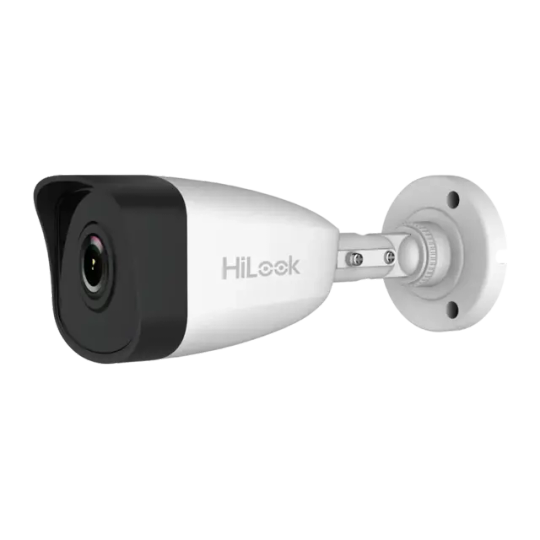
HiLook 1.0MP Bullet IP Cam 4.0mm Key Features 1/4" progressive scan CMOS Up to 1.0 megapixel 2.8 mm/4 mm/6 mm fixed focal lens Up to 30 m IR range Dual stream Digital WDR (Wide Dynamic Range) 3D DNR (Digital Noise Reduction) PoE (Power over Ethernet) IP67 Mobile monitoring via Hik-Connect or iVMS-4500 Specification Camera Image Sensor: 1/4" progressive scan CMOS Min. Illumination: Color: 0.01 Lux @(F1.2, AGC ON), 0 Lux with IR Shutter Speed: 1/3 s to 1/100, 000 s, support slow shutter Day &Night: IR cut filter with auto switch Wide Dynamic Range: Digital WDR Angle Adjustment: Pan: 0° to 360°, tilt: 0° to 180°, rotation: 0° to 360° DNR: 3D DNR Lens Lens 2.8 mm @F2.2, horizontal field of view 92°, 4 mm @F2.2, horizontal field of view 70° 6 mm @F2.2, horizontal field of view 56° Lens Mount M12 Illuminator IR Range: Up to 30 m Network Alarm Trigger: Video tampering, network disconnected, IP address conflicted Protocols: TCP/IP, ICMP, HTTP, HTTPS, FTP, DHCP, DNS, DDNS, RTP, RTSP, RTCP, NTP, UPnP, SMTP, IGMP, 802.1X, QoS, IPv6, Bonjour Video Max. Resolution: 1280 × 720 Video Compression Main stream: H.264 Sub stream: H.264/MJPEG H.264 Type: Baseline profile/Main profile Video Bit Rate: 32 Kbps to 2 Mbps Smart Feature-Set Basic EventMotion detection Image Image Setting: Brightness, saturation, contrast, sharpness are adjustable via web browser or client software Day/Night Switch: Support auto, scheduled Main Stream Max. Frame Rate 50Hz: 25fps @(1280 × 720) 60Hz: 30fps @(1280 × 720) Others: Mirror, BLC (area configurable), region of interest (support 1 fixed region) Sub-Stream Max. Frame Rate 50Hz: 25fps @( 640 × 480, 352 × 288, 320 × 240) 60Hz: 30fps @( 640 × 480, 352 × 240, 320 × 240) 4G Standard: ONVIF (PROFILE S), ISAPI Interface Communication Interface: 1 RJ45 10M/100M self-adaptive Ethernet port General General Function: Anti-flicker, heartbeat, mirror, password protection, privacy mask, watermark Startup And Operating Conditions: -30 °C to 60 °C (-22 °F to 140 °F), humidity: 95% or less (non-condensing) Power Supply: 12 VDC ±25%, PoE (802.3af) Power Consumption And Current 12 VDC, 0.3 A, Max. 4 W PoE (802.3af, 37 V to 57 V), 0.08 A to 0.13 A, Max. 5 W Dimensions: 69.1 mm × 66 mm × 172.7 mm ( 2.7" × 2.6" × 6.8") Weight: 500 g (1.1 lb.) Interface Protection: IP67
0 notes
Text
9 best mirrorless cameras (2025): Full-frame, APS-C, and more
Nikon's Z6 III offers most of the top features of the Z8 and Z9 more expensive than Nikon for the Z6 series. Z6 III (8/10, wired recommended) There is Nikon 24 -megapixel CMOS sensor, 3D theme monitoring system very quickly and accurately and encrypted Prores for the video, making it one of the best images, images/videos on the market. school. The bits that are partially ranked by the Viking…
0 notes
Text
GigE Camera Market 2022 | Present Scenario and Growth Prospects 2032
The global GigE camera market size is anticipated to develop at a CAGR of 9.1% from 2022 to 2032, reaching US$ 5.8 billion. In 2022, its estimated worth will be US$ 3.5 billion. Sales of GigE cameras are expected to increase in the coming years as a result of these cameras’ capacity to transport data swiftly during certain tasks that call for the use of numerous cameras.
GigE Camera or Gigabit Ethernet Camera is the image camera which has an ability to interface with computer system using GigE port. GigE cameras are based on GigE vision standards developed specifically for cameras which transmit images over gigabit Ethernet.
GigE cameras have ability to transfer data up to 1000MB/s which makes it favourable for many demanding applications. GigE cameras are predominantly used for applications which requires high rate of data transfer through long cable distances.
The GigE camera is a very affordable solution with simple configuration possibilities because it does not require a frame grabber, unlike many previous interface technologies. Over the course of the forecast period, all of these benefits are anticipated to contribute to the GigE camera market’s swift expansion.
GigE Camera Market: Drivers & Restraints
GigE camera market is expected to show significant growth during the period of forecast. Factors which are driving the growth of global GigE camera market are fast data transfer speed, decreasing development cost and efficient video transmission with easier configuration options.
On the other hand, increased CPU load and necessity of universal driver for interoperability are the restraints for the growth of global GigE camera market. However, adoption of 3D vision technologies and move towards smart camera based system creates great opportunity for global GigE camera market
GigE Camera Market: Region wise outlook
By region, the global GigE camera market can be segmented into seven regions namely, North America , Latin America, Asia-Pacific excluding Japan, Western Europe, Japan as a separate region, Eastern Europe and Middle East & Africa. Out of all this regions, present global GigE camera market is dominated by North America region in terms of value.
In North America region, non-manufacturing applications of GigE cameras such as security & surveillance, intelligent transportation and medical imaging are dominating. It is mainly because of high infrastructural development and high adoption of advanced technology. On the other hand Asia Pacific region is estimated to grow rapidly during the period of forecast.
Market Competition
Some of the key players operating in the global GigE camera are Toshiba Corporation, Allied Vision Technologies GmbH, Sony Corporation, Basler AG, Teledyne DALSA Inc., Baumer, Qualitas Technologies, IMPERX, Inc., Omron Corporation, and Matrox Imaging.
The global market is highly fragmented with the presence of several renowned companies providing their in-house products. Many vendors are focusing on the rapid adoption of the new product launch strategy with less product differentiation in terms of offerings. A few other key players are aiming to engage in mergers and acquisitions with start-up companies and local firms to strengthen their footprint in the global market.
Request a Sample of this Report https://www.futuremarketinsights.com/reports/sample/rep-gb-715
Key Segments Profiled in the GigE Camera Industry Survey
By Technology:
Complementary Metal- Oxide — Semiconductor (CMOS)
Charge Coupled Device (CCD)
By Type:
Line Scan
Area Scan
By Color Sensor Type:
Color
Monochrome
By End User:
Military and Defense
Industrial
Pharmaceutical
Traffic, Security & Surveillance
Medical/Life Sciences
Others
By Region:
North America
Latin America
Western Europe
Eastern Europe
APEJ
Japan
Middle East and Africa
0 notes
Text
0 notes