#CircuitBoardAssembly
Explore tagged Tumblr posts
Visit Tumblr Blog
Explore Tumblr blogs with no restrictions, modern design and the best experience.
Last Seen Tumblr Blogs


Fun Fact
Tumblr was created by web developers David Karp and Marco Arment.
Text
Printed Circuit Board Manufacturers
Introduction
In today's technological landscape, printed circuit boards (PCBs) are at the heart of countless electronic devices. Whether it's smartphones, computers, or medical equipment, PCBs play a critical role in connecting and powering various components. When it comes to choosing a PCB manufacturer, it's essential to find a reliable partner that can meet your specific requirements. In this article, we will explore the top 4 PCB manufacturers in the USA, highlighting their strengths and capabilities.
What is a PCB?
Before diving into the details, let's briefly understand what a PCB is. A printed circuit board is a flat board made of non-conductive material, usually fiberglass, with copper tracks etched or printed onto it. These tracks serve as electrical pathways, connecting different electronic components such as resistors, capacitors, and integrated circuits. PCBs provide mechanical support and facilitate the efficient flow of electrical signals, making them vital in modern electronic devices.
Importance of choosing the right PCB manufacturer
Choosing the right PCB manufacturer is crucial for the success of any electronic product. The quality, reliability, and performance of the PCB can significantly impact the overall functionality and longevity of the device. A reputable manufacturer ensures that the PCBs are manufactured to meet industry standards, undergo thorough testing, and are built to withstand various environmental conditions.
Factors to consider when choosing a PCB manufacturer
When selecting a PCB manufacturer, several factors should be taken into consideration:
Quality and reliability: Look for manufacturers with a track record of producing high-quality and reliable PCBs. Quality control measures, certifications, and adherence to industry standards are indicators of a manufacturer's commitment to excellence.
Manufacturing capabilities: Assess the manufacturer's manufacturing capabilities, including equipment, production capacity, and technological expertise. This ensures they can handle your specific project requirements effectively.
Technical support and customer service: Good technical support and responsive customer service are invaluable when it comes to resolving any issues or addressing concerns throughout the PCB manufacturing process.
Pricing and lead times: Evaluate the manufacturer's pricing structure and lead times to ensure they align with your project budget and timeline. Balancing cost-effectiveness with timely delivery is crucial.
Visit for more information on PCB Manufacturers: https://www.acmecircuit.com/blog/
#PCBManufacturers#PCBManufacturing#PrintedCircuitBoard#CircuitBoardAssembly#CircuitBoardManufacturing#PCBBoardManufacturer#HighFrequencyPCB#PCBManufacturersNearMe#PCBManufacturer#PCBSupplier#PCBAssemblyServices#PCBAssemblyManufacturer#ElectronicCableAssembly#ElectronicContractServices#PCBExporters#PrintedCircuitBoardManufacturer#PCBManufacturingCompanies#PCBManufacturerIndia#PCBIndustry#PCBSolutions#ElectronicManufacturing#PCBPrototyping#PCBDesign#ElectronicsProduction#PCBQualityControl#ElectronicsEngineering#PCBTechnology#PCBExperts#PCBInnovation#PCBManufacturingProcess
0 notes
Text

#circuitboardassembly#circuitboardtexture#circuitboardsmanufacturing#circuitboardcomponents#Circuitboardrepair
0 notes
Link
Multiple circuits’ combination involves various logic gates to create a multiplexer, encoder, de-multiplexer, and decoder. Such circuits have certain qualities, such as the circuit's output more depends on the levels which are present at the input terminal.
Such a circuit lacks memory, and the previous input can’t influence the current input. The combined circuits consist of inputs and outputs.
A half adder is an electronic circuit that adds two binary numbers. So, two single binary numbers act as adders in this case. It can return the carry and the output, and the representation in practice involves the XOR and AND logic gates. There are two inputs in a half adder circuit, including A and B, generating the Sum and Carry. So, the number of outputs is also two in this case, like S and C.
Website: https://pnconline.com/ Facebook: https://www.facebook.com/PNCONLINE Twitter: https://twitter.com/PNCINC Instagram: https://www.instagram.com/pnc_pcb/ Tumblr: https://www.tumblr.com/blog/view/pncinc Myspace: https://myspace.com/pncinc2020 Bresdel: https://bresdel.com/pncinc Call us: (973) 284-1600 Email us: [email protected] Location: PNC INC, 115 East Centre St.Nutley, NJ, 07110
0 notes
Link

#pcb assembly#PCB#PCBAssemblyServices#PCBAssemblyCompany#PrintedCircuitBoardAssembly#CircuitBoardAssembly#PCBManufacturing#pcbassemblycapabilities#PrototypePCBAssemblyManufacturing#technotronix#California#OrangeCounty#Riverside#LosAngeles
0 notes
Text
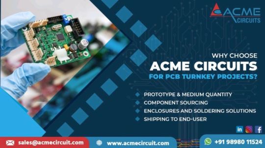
Top PCB Manufacturers In India

https://www.acmecircuit.com Are providers of top quality printed circuit board suppliers, printed circuit board manufacturers & rigid boards suppliers, etc at the industrial level at reasonable rates. For more info please contact us at (+91 98980 11524)
#PCBManufacturers#PCBManufacturing#PrintedCircuitBoard#CircuitBoardAssembly#CircuitBoardManufacturing#PCBBoardManufacturer#HighFrequencyPCB#PCBManufacturersNearMe#PCBManufacturer#PCBSupplier#PCBAssemblyServices#PCBAssemblyManufacturer#ElectronicCableAssembly#ElectronicContractServices#PCBExporters#PrintedCircuitBoardManufacturer#PCBManufacturingCompanies#PCBManufacturerIndia#PCBIndustry#PCBSolutions#ElectronicManufacturing#PCBPrototyping#PCBDesign#ElectronicsProduction#PCBQualityControl#ElectronicsEngineering#PCBTechnology#PCBExperts#PCBInnovation#PCBManufacturingProcess
1 note
·
View note
Text
Four Stages of PCB Design and Assembling
PCB is a printed circuit board that helps connect different electrical components. The board is a combination of laminated material, and the copper foil laid on a non-conductive substrate.
A PCB is the main part of any electronic device, so it has to be perfect. It should have functional components and microelectronics circuits to perform well. Development of PCB goes through different processes that you should know well. PCB manufacturing has 4 stages, including design, manufacturing, PCB assembly, and PCB testing.
First Stage- Design
PCB design involves different steps, such as schematic design, layout planning, the placement of the components, routing, and manufacturing files.
PCB schematic design: It is a blueprint of PC design that shows all PCB components with symbols. The schematic design is always according to the technical requirements of the user.
Layout planning: After the schematic design, you have to develop the layout of a PCB that includes physical components’ models, the shape of the PCB, and the structure of a PCB.
Placement of components: It involves planning the placement of various components. You decide on the PCB layers according to your requirements. The right placement of the components ensures a flawless board, decreasing the production cost.
First of all, the designer places the fixed components in the layout, including switches and connectors.
Then, the critical components are placed, such as memory chips, microprocessors, as well as power supplies.
Then the supporting components of the PCB are placed, like inductors, capacitors, and resistors.
In the end, the decoupling capacitors and terminating resistors are placed.
Routing: Once the components are placed, you have to connect all components through trace routing. There are four ways to do so, such as manual routing, auto-interactive routing, semi-automatic, and batch-auto routing. You can choose any method according to your Printed Circuit Board and budget.
Design: In this stage, you have to plan for the number of board layers, dimension of the board, and types of components. You can use a special app in this case, such as EDA or electronic design automation. The designer often adopts the SMT instead of a through-hole technology, depending on your requirements.Once the design is over, you can export the design files to CAD or Gerber format.
Preparation of manufacturing files: This is the last stage of design where the designer exports the Gerber files for manufacturing. The manufacturer needs these files to develop a printed circuit board.
Stage 2-Manufacturing of Circuit Board
Once the manufacturer receives all design drawings, he starts making PCB. It involves different stages as described below:
Design Imaging: The manufacturer uses a plotter to convert the PCB design files into filmslike they resemble the photo negatives of the schematic design. The printer uses black and clear inks for inner and outer layers. Copper traces and circuits are shown with black ink, whereas the non-conductive parts are shown with clearink.
Printing of Inner Layers on Copper: It is the initial stage of PCB manufacturing. The engineer uses a substrate material to make a laminated board. Like, epoxy resin or fiberglasses are common in this case. The design of the PCB is printed on the board, and then his pre-bondscopper on a board’s both sides. After that comes the etching of copper, and then the board is protected through a photo-sensitive film.
Ultraviolet Light: the manufacturer then exposes the resist-covered PCB to UV light to strengthen the photo-reactive material. Then the board is cleaned with an alkaline solution to get rid of unnecessary copper particles. The expert checks the board to remove any errors and then goes to the next stage. The main aim of UV blasting is to develop a PCB Board according to the schematic drawing.
Inner layer’s etching: copper’s inner layer needs chemical etching for removal. The process of photoresist prevents the essential copper from etching. The board size determines the amount of the solution and etching time which is less for small boards but more for large boards.
Some other manufacturing processes include:
· Alignment of layers
· Optical testing
· Layer pressing and lamination
· Drilling
· Plating of PCB
· Imaging of external layer
· Etching of external layer
· Solder mask
· Silk screening
· PCB finishing
· Testing
· Profiling
· Quality testing
· Packaging of PCB
· Shipping of PCB
Stage 3-PCB Assembly
The assembly of a PCB involves four stages, such as soldering, placement of components, solder pasting, and testing. Let’s review them in detail.
Solder Pasting: It is like t-shirt screening, as it involves solder paste stenciling. The stencil is made of stainless steel and it’s very thin. You have to use the stencil to apply the paste in areas where different components will be installed. In this process, flux is used for melting the paste to help it bond to the PCB.
Placementofthe Components: Once you are done with the solder paste, you need a pick and place the tool for the components. Generally, it is SMT or surface mount technology where components are placed on the PCB surface. Initially, it used to be a manual process and assemblers used tweezers to pick and place different components on the board. However, new technology has made this process automated due to robotics and it’s more precise and consistent.
Soldering of PCB: After the placement of components, you have to place the PCB on a conveyor belt to help a board move to a reflow oven that heats the board. The heating helps melt the solder paste, and bond the components on the board permanently. However, if the board has more components other than SMDs, it would need a through-hole insertion that involves more advanced soldering.
Testing of PCB Quality: Sometimes, the components are misplaced during reflow when the PCB is moving. This issue may cause a poor connection, or no connection at all, or the parts are not well-connected. So, you need to inspect the PCB to ensure a flawless function. A PCB can fail this test even if it passed other tests, and a failed PCB goes to scrap or you have to recycle it with all essential processes until you get a flawless circuit board.
Stage4-PCB Testing
Manufacturers use different methods for PCB testing to ensure that it will function correctly. These methods include in-circuit, optical inspection, flying probe, turn-in, x-ray, anda functional test.
In-Circuit: It is also known as ICT, or you can call it the bed-of-nails inspection. In this method, PCB is pressed on the bed of probes. It is highly accurate because it checks all components of a PCB. You can also test the BGAs with this method. Moreover, it also tests the solder integrity of the bottom-terminated components.
However, this test is expensive and time-consuming. Moreover, it does not test the non-electrical parts and connectors.
AOI, Automated Optical Inspection: This testing method involves a visual inspection of the board. It is done with the help of HD cameras, LED lights, UV, and high-level infrared. The test is contact-free and helps check poor solder joints or missing parts. It also tests the smt assembly issues and it’s very accurate.
However, it only inspects the preprogrammed errors and can’t check defects regarding glue or sealing.
Flying Probe Test: It involves probes that help test the upper and lower surface of a PCB. This PCB testing method is cost-effective, consumes less time, is easy to do, and is compatible with many applications of PCB assembly. However, it is slower than other testing methods and not ideal for complex testing.
Burn-In Test: In this test, PCB is exposed to a high temperature to see if it works well. It ensures a lifetime product and enhances the brand because of an effective end product.
However, this test is costly and can affect a PCB by damaging its components. Moreover, it can be less reliable due to voltage scaling.
Inspecting Through X-Ray: It involves an x-ray machine that inspects a PCB. It thoroughly checks soldering which is hard to detect with AOI. The x-ray inspection is ideal for thick or multilayered PCBs. It also detects the voids or bubbles and can also check the components under a shield.
However, it needs expensive x-ray machinesand can cause hazards in the workplace.
Functional Test ofPCB: It involves functional testers that you connect to the edge connector. It creates an electronic environment for which a PCB is made. It inspects the functional errors and identifies the analog issues. It also checks issues with digital circuitry.
However, it is very costly and needs high-end tools, which are too expensive. It needs a proper understanding of the working atmosphere of the DUT.
Final Thoughts
The development of a PCB involves different processes, including design, printing, assembling, and testing. Each stage is further divided into different parts, and you have to understand all stages to create a flawless PCB.
The board is a combination of laminated material, and the copper foil laid on a non-conductive substrate. A PCB is the main part of any electronic device, so it has to be perfect.
Would like to know more about the design or pcb assembly services stages? Email us at [email protected]
Website: https://pnconline.com/ Facebook: https://www.facebook.com/PNCONLINE Twitter: https://twitter.com/PNCINC Instagram: https://www.instagram.com/pnc_pcb/ Tumblr: https://www.tumblr.com/blog/view/pncinc Myspace :https://myspace.com/pncinc2020 Bresdel: https://bresdel.com/pncinc Call us: (973) 284-1600 Email us: [email protected] Location: PNC INC, 115 East Centre St.Nutley, NJ, 07110
0 notes
Link
A microwave circuit refers to any electrical or electronic device which operates on microwaves or uses microwaves for its operation. Some examples include radar systems, satellite dishes, cell phone towers, and TV antennas among others. Such circuits are designed to operate at specific frequencies or bandwidths so that they do not interfere with each other.
A microwave is an electromagnetic wave of frequency between 1GHz and 30GHz. It falls under the band B, C, D, and E in IEEE standards. Microwaves occupy a large part of the entire RF spectrum as compared to other frequencies. The global demand for communication devices such as routers, DSL, and mobile phones has increased significantly due to technological advancements such as internet connectivity being provided by these devices and advancements in technology by small-sized electronic components that can operate at high frequencies. As a result, there is an increase in demand for microwave circuit design services.
Microwave PCBs have to meet certain requirements that have not changed even though the designs have.
Website: https://pnconline.com/ Facebook: https://www.facebook.com/PNCONLINE Twitter: https://twitter.com/PNCINC Instagram: https://www.instagram.com/pnc_pcb/ Tumblr: https://www.tumblr.com/blog/view/pncinc Myspace :https://myspace.com/pncinc2020 Bresdel: https://bresdel.com/pncinc Call us: (973) 284-1600 Email us: [email protected] Location: PNC INC, 115 East Centre St.Nutley, NJ, 07110
0 notes
Text
Microwave Printed Circuit Board Concept
A microwave circuit refers to any electrical or electronic device which operates on microwaves or uses microwaves for its operation. Some examples include radar systems, satellite dishes, cell phone towers, and TV antennas among others. Such circuits are designed to operate at specific frequencies or bandwidths so that they do not interfere with each other.
A microwave is an electromagnetic wave of frequency between 1GHz and 30GHz. It falls under the band B, C, D, and E in IEEE standards. Microwaves occupy a large part of the entire RF spectrum as compared to other frequencies. The global demand for communication devices such as routers, DSL, and mobile phones has increased significantly due to technological advancements such as internet connectivity being provided by these devices and advancements in technology by small-sized electronic components that can operate at high frequencies. As a result, there is an increase in demand for microwave circuit design services.
Microwave PCBs have to meet certain requirements that have not changed even though the designs have.
Understanding The Concept
So, what is microwave PCB? Simply put, it’s a pc boardthat incorporates circuitry optimized for frequency bands in which microwave signals are most commonly used. As the boards are designed specifically for such frequencies, they offer superior performance over traditional boards in terms of both design and reliability. Besides, their smaller size and lower overall weight make them perfect for use in applications where space and transportation costs are at a premium.
Why Microwave Technology?
The microwave portion of telecommunications is used for point-to-point voice and data communications. You can also use it for two-way radio, cable television, and telegraphy in a limited range of frequencies. As it allows information transmission at high speeds over long distances, it is very common in military organizations. For these reasons and more, microwave technology plays an essential role in today’s technological world.
As such, it was important that an efficient way to transmit microwaves be developed, the result was a device called a microstrip line. In short, when combined with other components, microstrip lines are what allow microwaves to travel great distances while maintaining optimal signal strength.
A microstrip line consists of three main parts, including a metal foil, dielectric material, and a ground plane. Metal foil serves as an antenna, and the dielectric material acts as a waveguide. Whereas the ground plane provides electrical shielding. These three elements are placed on top of one another and bonded together using heat or pressure, which creates a single unit known as a structure.
What Are The Factors That We Need To Consider While Selecting The Right Board?
Choosing a board for microwave design is not an easy task. There are several factors that we need to consider such as frequency, applications, and modes of use. There are three main types of boards, including through-hole, single-sided, and multi-layer boards. It is also very important that you pick out a board that matches your frequency range.
For example, you need a board with wider spacing between conducting tracks at higher frequencies than low frequencies. So, make sure that you select the right one depending on your frequency range.
The next thing that you need to look into is your application or project needs. Depending upon your requirement, you can go ahead with either through-hole or SMD-style component placement methods.
The final step in choosing a microwave PCB will be deciding on the thickness of the copper traces before the Circuit board fabrication process. You will have to choose according to your project needs whether thin or thick copper traces would be best suited for your application. But, keep in mind that thicker copper traces provide better current carrying capacity but they are more expensive than thinner ones. So, again it all depends on what kind of budget you have set aside for your project.
Every board has its unique features, so do check out every detail before buying one. A well-known feature of these boards is their ability to withstand high temperatures without getting damaged. This makes them ideal for high-temperature environments like ovens, motors, etc.
Another advantage of using these boards is their small size which makes them easy to handle and transport from one place to another. They also come with different pin configurations like double row, single row, and even no pin configuration options. Some of them also offer the ground plane on both sides which helps in reducing noise levels due to capacitive coupling.
In addition to all these advantages, most of these boards are made up of epoxy glass material that provides insulation against electric fields and other environmental factors.
Installation of Components onto A Microwave PCB
Let’s now take a quick look at how we can install our components onto a microwave PCB. First of all, get yourself ready by wearing safety glasses and gloves so that you don’t end up hurting yourself during installation. Make sure that you have gathered all the tools required for installation beforehand.
Next, remove any existing solder mask and protective coating from the surface of your board. Make sure that there is no dirt or dust present on it as well. If necessary clean it thoroughly with acetone and then wipe dry with a lint-free cloth or paper towel.
After doing so you can proceed to install the components onto it just like any other circuit board out there. Remember to always start with your smallest components first and work your way up to larger ones. Before soldering it is recommended that you apply a thin coat of flux on all surfaces where you are going to be placing your components. Then apply a little bit of solder paste on each pad and lastly place your component in position and heat it with a soldering iron.
Make sure that you inspect for proper alignment of your parts and if needed apply extra flux or reposition it until everything looks just right. Once you are satisfied with your results, it’s time to apply a generous amount of solder over all your components. Once you have done so, wait for it to cool down and that’s it.
How Do I Choose My Microwave PCB Manufacturer?
Before you start shopping for a company to make your circuit boards, there are a few things you should know. Here’s a quick rundown of some key questions you should ask yourself as you’re shopping around, such as:
· Does your board require special materials?
· Do you need services outside of just PCB manufacturing?
· How many layers do you need?
· What sort of electrical isolation is needed between high-voltage and low-voltage areas on your board?
· How much space will you need for mounting components?
Once you have answers to these questions, it will be easier to find a vendor that can meet all of your needs. Of course, in order to get accurate information from vendors about their capabilities, you may need to provide them with more details about your project than what we've provided here. They must understand exactly what kind of design you're working with so they can give you honest feedback about whether or not they're able to work with it.
What Is Hybrid Microwave Circuit
A hybrid microwave involves a thin film or thick film technology to construct different microwave circuits using a medium that can transmit signals. The medium, in this case, is mostly sapphire, alumina porcelain, ceramics of high level, or quartz.
There are two types of hybrid microwave circuits, passive and active. Passive hybrid circuits consist of passive elements like resistors, capacitors, inductors, and filters. Whereas active hybrid circuits use active devices like transistors, diodes, etc.
Active hybrid circuits have better performance than passive ones, but their fabrication process is more complex than passive ones because they contain semiconductor elements, unlike passive elements. Thus it is easier to fabricate passive hybrid circuits than active ones.
There are various factors affecting the microwave circuit design such as size, power consumption, cost of materials used, and the operating temperature. These factors must be considered while designing a microwave circuit.
Understanding the Lumped Componentization of a Microwave Circuit
A lumped component model is one of several techniques used to analyze and design high-frequency microwave circuits. It was originally developed for analysis and design in communication systems. It is characterized by using lumped elements (e.g., resistors, capacitors, inductors) instead of transmission lines or other forms of circuit elements whose behavior is dominated by distributed parameters like permittivity and permeability.
In addition to being useful for analysis, lumped element models are also useful for conceptual designs because they make it easier to visualize components and their interconnections. The concept of lumped element models is very similar to that of ideal transformers used in a single-sideband modulation. In this model, an ideal transformer represents an actual transformer with losses and non-ideal characteristics asleakage reactanceare replaced by zero values.
The equivalent circuit consists of an impedance connected between port 1 and the ground, plus a series capacitor representing the leakage reactance and shunt conductance. This technique is often referred to as lumped parameter modeling. Other examples include bridge networks used in an RF filter design and the current source inverters used in active filters.
Would like to know more about the Microwave PCB conceptor printed circuit board assembly? Email us at [email protected]
Website: https://pnconline.com/ Facebook: https://www.facebook.com/PNCONLINE Twitter: https://twitter.com/PNCINC Instagram: https://www.instagram.com/pnc_pcb/ Tumblr: https://www.tumblr.com/blog/view/pncinc Myspace :https://myspace.com/pncinc2020 Bresdel: https://bresdel.com/pncinc Call us: (973) 284-1600 Email us: [email protected] Location: PNC INC, 115 East Centre St.Nutley, NJ, 07110
0 notes
Link
Unlike a traditional PCB,HDI has high-density circuitry. It consists of different types of vias, including buried, blind, and micro-vias. Some other features of this PCB include:
· Surface to surface through vias
· HDI construction involves layer pairs
· Passive layers without electrical connection
· Minimum two layers having through vias
HDI PCBs are ideal for smart devices or electronics having less weight. You must hire an experienced manufacturer to have an HDI printed circuit board because it has very narrow tolerances. So, only experts can handle such a PCB, as a little defect can lead to serious issues.
What are the benefits of an HDI circuit board?
There are many advantages of the HDI printed circuit board, provided it is according to the design parameters. Your product can perform better with the HDI technology. Let’s study its benefits one by one.
It Needs Less Space
HDI circuit boards don’t take much space, so the overall weight of the final product is also less. You can have more components on a board’s both sides, getting a functional, small,and lighter device.
Better Electrical Function
You get an enhanced electrical performance through HDI because of a little distance between the components and more transistors. Such features involve less power consumption, resulting in better signals. The signal transmission becomes fast due to a smaller size, besides, there are lessercrossing delays and signal losses.
More Cost-Effective
Since an HDI PCBoard is smaller than traditional boards, it needs fewer raw materials, hence its cost is also less.Instead of having multiple PCBs in one product, a single HDI PCB is enough for better performance through small size and minimum material.
Quick Production
The production time is also faster than the conventional boards. Your product gets ready for selling if its construction involves an HDI printed circuit board having minimum materials. It is easy to place the components on HDI boards, moreover,better electrical performance is there toreduce the troubleshooting and testing time.
More Reliable
The microvias in the HDI PCB come up with small aspect ratios and involve high-quality manufacturing, making the board reliable. A reliable PCB is always cost-effective, so the end product is also reliable and satisfactory
What To Consider While Designing An HDI PCB
You have to consider certain factors and parameters while designing the HDI circuit board. The production of such a board is different from others that we will discuss below.
Lamination Process
High-density PC Board Fabrication involves sequential laminations where you have to combine the PCB layers or cores with copper and pre-set layers. It involves heat and pressure according to the type ofthe circuit board. Once the lamination is over, you need to drill vias several times, unlike a traditional PCB. So, such a sequential lamination process helps manufacturers have flawless drilling without any breaking or shifting.
Understanding The Via-In-Pad
The construction of the high-density PCB involves thevia-in-pad process to help you to make vias on a flat surface of your PCB. You have to plate vias, filling them in different ways, capping them, and then plating over them. The process of via-in-pad consists of 10 to 12 steps,and it needs skilled workers and special tools. There are many benefits of using the via-in-pad for HDI boards, including reduced space, simple thermal management, and less time to bypass the capacitors,in the case of high-frequency layout designs.
Considering Via Fills
You should also consider the type of via fill as it has to be compatible with the PCB requirements and its application. Some common filling materials, in this case, include electrochemical plating, copper, silver, and conductive and non-conductive epoxy of which non-conductive epoxy is highly used. Moreover, via fill should be flushed with the flat surface of the PCB and should also be fully soldered.
The via fill helps develop the blind, buried, and drilled vias in the case of both standard and microvias. Then comes via plating to hide it under the SMT surface. It involves several drill cycles at balanced depths to have precise drilling. Such well-controlled drilling needs special tools and more time.
Layout Options
You will see the HDI circuit boards having different layout designs, including
· 1-n-1 PCB
· 2-n-2 PCB
A 1-n-1 PCB is the simplest HDI circuit board as it is a single construction of multiple layers of high density. These layers are interconnected, and such a board needs sequential lamination on both sides of the core. Whereas the 2-n-2 PCB consists of two layers of high density to help you to stack microvias around the layers. The microvias have copper filling in the case of complex layout designs.
The HDI structure can reach high levels of X-n-X even though its complexity and cost limit the construction. There is also the any-layer HDIwith a very dense layout where conductors can interconnect easily through laser microvias. You will see such designs in CPU and GPU chips, like in many mobile devices and smartphones
Laser Drilling
When it comes to the any-layer HDI, you will have to apply the laser drills to create microvias. In this process, the drill emits a laser of 20 microbe diameter which can easily cut the glass or metal, providing small and clean vias. You can also use the uniform glass to make very small holes, as such a glass type has a low dielectric constant.
Website: https://pnconline.com/ twitter.com: https://twitter.com/PNCINC pinterest.com: https://www.pinterest.com.au/rrosh2014/_created/ Facebook.com: https://www.facebook.com/PNCONLINE myspace.com: https://myspace.com/pncinc2020 tumblr.com: https://www.tumblr.com/blog/view/pncinc instagram.com: https://www.instagram.com/pnc_pcb/ bresdel.com: https://bresdel.com/pncinc Location: 115 East Centre St. Nutley, NJ, 07110 Call us: (973) 284-1600 Email us: [email protected]
0 notes
Link
Multiple circuits’ combination involves various logic gates to create a multiplexer, encoder, de-multiplexer, and decoder. Such circuits have certain qualities, such as the circuit's output more depends on the levels which are present at the input terminal.
Such a circuit lacks memory, and the previous input can’t influence the current input. The combined circuits consist of inputs and outputs.
A half adder is an electronic circuit that adds two binary numbers. So, two single binary numbers act as adders in this case. It can return the carry and the output, and the representation in practice involves the XOR and AND logic gates. There are two inputs in a half adder circuit, including A and B, generating the Sum and Carry. So, the number of outputs is also two in this case, like S and C.
Website: https://pnconline.com/ Facebook: https://www.facebook.com/PNCONLINE Twitter: https://twitter.com/PNCINC Instagram: https://www.instagram.com/pnc_pcb/ Tumblr: https://www.tumblr.com/blog/view/pncinc Myspace: https://myspace.com/pncinc2020 Bresdel: https://bresdel.com/pncinc Call us: (973) 284-1600 Email us: [email protected] Location: PNC INC, 115 East Centre St.Nutley, NJ, 07110
0 notes